LB11850VA
Single‐phase Full‐wave
Pre‐driver with Speed
Control Function
for Fan Motor
www.onsemi.com
Monolithic Digital IC
Overview
The LB11850VA is a single-phase bipolar fan motor driver with
speed control function that works with a speed feedback signal.
A highly efficient, quiet and low power consumption motor driver
circuit, with a high speed accuracy and large variable speed can be
implemented by adding a small number of external components.
This pre-driver is optimal for driving large scale fan motors (with
large air volume and large current) such as those used in servers and
consumer products.
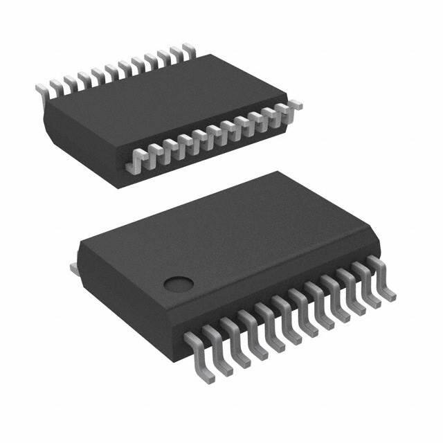
SSOP24
CASE 565AR
MARKING DIAGRAM
Functions and Features
• Pre-driver for Single-phase Full-wave Drive
PMOS-NMOS is Used as an External Power TR, Enabling
High-efficiency and Low-power-consumption Drive by Means
of the Low-saturation Output and Single-phase Full-wave Drive
On-chip Speed Control Circuit
♦ The Speed Control (Closed Loop Control) Using a Speed
Feedback Signal Makes it Possible to Achieve Higher Speed
Accuracy and Lower Speed Fluctuations when Supply Voltage
Fluctuates or Load Fluctuates, Compared with an Open-loop
Control System. Separately Excited Upper Direct PWM Control
Method is Used as the Variable-speed Control System
External PWM Input or Analog Voltage Input Enabling Variable
Speed Control
♦ The Speed Control Input Signal is Compatible with PWM Duty
Ratio or Analog Voltages
On-chip Soft Start Circuit
Lowest Speed Setting Pin
♦ The Lowest Speed can be Set with the External Resistor
Current Limiter Circuit Incorporated
♦ Chopper Type Current Limit at Start or Lock
Reactive Current Cut Circuit Incorporated
♦ Reactive Current before Phase Change is Cut to Enable Silent and
Low-consumption Drive
Constraint Protection and Automatic Reset Functions Incorporated
FG (Speed Detection), RD (Lock Detection) Output
Constant-voltage Output Pin for Hall Bias
XXXXXXXXXX
YMDDD
♦
•
•
•
•
•
•
•
•
•
XXXXX
Y
M
DDD
= Specific Device Code
= Year
= Month
= Additional Traceability Data
PIN ASSIGNMENT
24
1
OUT2P
OUT1P
OUT2N
OUT1N
VCC
SGND
5VREG
SENSE
CVI
C
CVO
EO
CTL
EI
RC
LIM
SOFT
CT
CPWM
IN+
FG
HB
RD
IN−
12
(Top View)
13
ORDERING INFORMATION
See detailed ordering and shipping information on page 14 of
this data sheet.
© Semiconductor Components Industries, LLC, 2013
March, 2018 − Rev. 1
1
Publication Order Number:
LB11850VA/D
�LB11850VA
SPECIFICATIONS
ABSOLUTE MAXIMUM RATINGS (TA = 25°C)
Symbol
VCC max
Parameter
Conditions
Ratings
Unit
VCC Maximum Supply Voltage
18
V
IOUTN max
OUTN Pin Maximum Output Current
20
mA
IOUTP max
OUTP Pin Maximum Sink Current
20
mA
VOUT max
OUT Pin Output Withstand Voltage
18
V
HB
HB Maximum Output Current
10
mA
CTL, C max
CTL, C Pin Withstand Voltage
7
V
CVI, LIM Pin Withstand Voltage
7
V
RD/FD Output Pin Output Withstand
Voltage
19
V
RD/FG Output Current
10
mA
CVI, LIM max
FG max
I5VREG max
Pd max
5VREG Pin Maximum Output Current
Allowable Power Dissipation
Mounted on a specified board (Notes 1, 2)
10
mA
0.9
W
Topr
Operating Temperature Range
−30 to +95
°C
Tstg
Storage Temperature Range
−55 to +150
°C
Stresses exceeding those listed in the Maximum Ratings table may damage the device. If any of these limits are exceeded, device functionality
should not be assumed, damage may occur and reliability may be affected.
1. Mounted on a specified board: 114.3 mm × 76.1 mm × 1.6 mm, glass epoxy.
2. Tj max = 150_C. Use the device in a condition that the chip temperature does not exceed Tj = 150_C during operation.
RECOMMENDED OPERATING RANGES (TA = 25°C)
Parameter
Symbol
Conditions
Ratings
Unit
VCC1
VCC Supply Voltage 1
VCC pin
5.5 to 16
V
VCC2
VCC Supply Voltage 2
When VCC − 5VREG shorted
4.5 to 5.5
V
VCTL
CTL Input Voltage Range
0 to 5VREG
V
VLIM
LIM Input Voltage Range
0 to 5VREG
V
VCVI
VCI Input Voltage Range
0 to 5VREG
V
VICM
Hall Input Common Phase Input Voltage
Range
0.2 to 3
V
Functional operation above the stresses listed in the Recommended Operating Ranges is not implied. Extended exposure to stresses beyond
the Recommended Operating Ranges limits may affect device reliability.
ELECTRICAL CHARACTERISTICS (TA = 25°C, VCC = 12 V, unless otherwise specified)
Parameter
Symbol
ICC1
Circuit Current
ICC2
5VREG
Typ
Max
Unit
During drive
Conditions
Min
12
15
mA
During lock protection
12
15
mA
5VREG Voltage
I5VREG = 5 mA
4.8
5.0
5.2
V
VHB
HB Voltage
IHB = 5 mA
1.05
1.20
1.35
V
VLIM
Current Limiter Voltage
190
210
230
mV
VCRH
CPWM Pin H Level Voltage
2.8
3.0
3.2
V
VCRL
CPWM Pin L level Voltage
0.9
1.1
1.3
V
ICPWM1
CPWM Pin Charge Current
VCPWM = 0.5 V
24
30
36
mA
ICPWM2
CPWM Pin Discharge Current
VCPWM = 3.5 V
21
27
33
mA
FPWM
CPWM Oscillation Frequency
C = 220 pF
30
www.onsemi.com
2
kHz
�LB11850VA
ELECTRICAL CHARACTERISTICS (TA = 25°C, VCC = 12 V, unless otherwise specified) (continued)
Symbol
Parameter
Conditions
Min
Typ
Max
Unit
VCTH
CT Pin H Level Voltage
2.8
3.0
3.2
V
VCTL
CT Pin L Level Voltage
0.9
1.1
1.3
V
ICT1
CT Pin Charge Current
VCT = 2 V
1.6
2.0
2.5
mA
ICT2
CT Pin Discharge Current
VCT = 2 V
0.16
0.20
0.25
mA
RCT
CT Pin Charge/Discharge Current
Ratio
ICT1/ICT2
8
10
12
times
OUTN Pin Output H Voltage
IO = 10 mA
−
VCC−0.85
VCC−1.0
V
VONL
OUTN Pin Output L Voltage
IO = 10 mA
−
0.9
1.0
V
VOPL
OUTP Pin Output L Voltage
IO = 10 mA
−
0.5
0.65
V
VHN
Hall Input Sensitivity
IN+, IN− difference voltage
(including offset and hysteresis)
−
±15
±25
mV
VFGL
FG Output L Voltage
IFG = 5 mA
−
0.15
030
mA
IFGL
FG Pin Leak Current
VFG = 19 V
−
−
30
mA
VRDL
RD Output L Voltage
IRD = 5 mA
−
0.15
0.30
V
IRDL
RD Pin Leak Current
VRD = 19 V
−
−
30
mA
VEOH
EO Pin Output H Voltage
IEO1 = −0.2 mA
VREG−1.2
VREG−0.8
−
V
IEO1 = 0.2 mA
VONH
VEOL
EO Pin Output L Voltage
−
0.8
1.1
V
VRCH
RC Pin Output H Voltage
3.2
3.45
3.7
V
VRCL
RC Pin Output L Voltage
0.7
0.8
1.05
V
RC Pin Clamp Voltage
1.3
1.5
1.7
V
VCTLH
CTL Pin Input H Voltage
2.0
−
VREG
V
VCTLL
CTL Pin Input L Voltage
0
−
1.0
V
VCTLO
CTL Pin Input Open Voltage
VREG−0.5
−
VREG
V
ICTLH
CTL Pin H Input H Current
VFGIN = 5VREG
−10
0
10
mA
ICTLL
CTL Pin L Input L Current
VFGIN = 0 V
−120
−90
−
mA
VRCCLP
VCH
C Pin Output H Voltage
VREG−0.3
VREG−0.1
−
V
VCL
C Pin Output L Voltage
1.8
2.0
2.2
V
IBLIM
LIM Pin Input Bias Current
−1
−
1
mA
VILIM
LIM Pin Common Phase Input
Voltage Range
2.0
−
VREG
V
ICSOFT
SOFT Pin Charge Current
1.0
1.3
1.6
mA
VISOFT
SOFT Pin Operating Voltage
Range
2.0
−
VREG
V
IB(VCI)
CVI Pin Input Bias Current
−1
−
2
mA
CVI Pin Common Phase Input
Voltage Range
2.0
−
VREG
V
−
V
2.2
V
VIVCI
VOH(VCO)
CVO Pin Output H Level Voltage
VOL(VCO)
Output L Level Voltage
VREG−0.35 VREG−0.2
1.8
2.0
Product parametric performance is indicated in the Electrical Characteristics for the listed test conditions, unless otherwise noted. Product
performance may not be indicated by the Electrical Characteristics if operated under different conditions.
3. Design target value and si not measured.
www.onsemi.com
3
�LB11850VA
1.2
Mounted on a specified board:
114.3 × 76.1 × 1.6 mm
glass epoxy
Allowable Power Dissipation,
Pd max − W
1.0
0.9
0.8
0.6
0.4
0.2
0.0
−30
0
90 95
60
30
120
Ambient Temperature, TA − 5C
Figure 1. Pd max − TA
TRUTH TABLE − LOCK PROTECTION CPWM = H
IN−
IN+
CT
OUT1P
OUT1N
OUT2P
OUT2N
FG
Mode
H
L
L
L
L
OFF
H
L
OUT1 → 2 drive
L
H
OFF
H
L
L
OFF
OUT2 → 1 drive
OFF
L
OFF
H
L
Lock protection
OFF
H
OFF
L
OFF
OUT1P
OUT1N
OUT2P
OUT2N
Mode
H
L
L
H
H
TRUTH TABLE − SPEED CONTROL CT = L
EO
CPWM
IN−
L
H
H
L
L
L
OFF
H
OUT1 → 2 drive
L
H
OFF
H
L
L
OUT2 → 1 drive
H
L
OFF
L
OFF
H
Regeneration mode
L
H
OFF
H
OFF
L
H
L
IN+
www.onsemi.com
4
�VCC
5
www.onsemi.com
Figure 2. Block Diagram
CTL
signal
CTL
C
CVO
CVI
SOFT
LIM
RC
5VREG
VCC
CTL
VREF
1shot−
multi
VREG
EI
EDEG
Thermal
shut down
FG
EO
FG
RD
IN+
IBL01797
HALL
HB
HallBias
CT
IN−
CPWM
Oscillation
CONTROL
CIRCUIT
SENSE
5VREG
Discharge circuit
GND
OUT2P
OUT2N
OUT1P
OUT1N
LB11850VA
BLOCK DIAGRAM
�LB11850VA
APPLICATION CIRCUIT
*3
1 mF/25 V
Rp = 1 kW
1)
3)
2)
4)
100 W
RF
1 mF/25 V
RFG/RPD =
10 kW to 100 kW
*2
V CC
5VREG
*9
FG
RD
RC
*8
*7
SENSE
LIM
LB11850VA
SOFT
CVI
CVO
OUT1P
1)
OUT1N
2)
OUT2P
3)
OUT2N
4)
HB
IN−
C
CTL signal
*4
IN+
CTL
CT
*5
EI
EO
CPWM
SGND
*1
Figure 3. Sample Application Circuit
www.onsemi.com
6
H
*6
CT = 1 mF
CP = 220 pF
30 kHz
�LB11850VA
DESCRIPTION OF PRE-DRIVER BLOCK
*6:
This is the pin to connect capacitor for lock
detection.
Constant-current charging and constant-current
discharging circuits are incorporated. When the
pin voltage becomes 3.0 V, the safety lock is
applied, and when it lowers to 1.0 V, the lock
protection is reset.
Connect this pin to GND when it is not in use
(when lock protection is not required).
*7:
This is the pin for current limiter detection.
When the pin voltage exceeds 0.21 V, current
limiting is applied, and the low-side regeneration
mode is established.
Connect this pin to GND when it is not in use.
*8:
Lock detection pin.
This is the open collector output, which outputs
“L” during rotation and “H” at stop. This pin is left
open when it is not in use.
*9:
Speed detection pin.
This is the open collector output, which can detect
the rotation speed using the FG output according
to the phase change. This pin is left open when it
is not in use.
*1:
SGND is connected to the control circuit power
supply system.
*2:
For the signal-side power stabilization capacitor,
the capacitance of more than 0.1 mF is used.
Connect the capacitor between VCC and GND with
the thick pattern and along the shortest route.
*3:
For the power-side power stabilization capacitor,
the capacitance of more than 0.1 mF is used.
Connect the capacitor between power-side power
supply and GND with the thick pattern and along
the shortest route.
*4:
Hall signal input pins.
Wiring needs to be short to prevent carrying noise.
If noise is carried, insert a capacitor between IN+
and IN−. The Hall input circuit is a comparator
having a hysteresis of 15 mV.
It has a ±30 mV (input signal difference voltage)
soft switch zone.
It is recommended that the Hall input level is
100 mV (p−p) at the minimum.
*5:
This is the pin to connect capacitor for generating
the PWM basic frequency.
Use of CP = 220 pF produces oscillation at the
frequency of 30 kHz which serves as the PWM
basic frequency.
Since this pin is also used for the current limiter
reset signal, the capacitor must be connected
without fail even when no speed control is
implemented.
www.onsemi.com
7
�LB11850VA
DESCRIPTION OF SPEED CONTROL BLOCK
1. Speed Control Diagram
The speed slope is determined by the constant of the RC pin.
(RPM)
CR time constant large
CR time constant small
Rotation speed
Minimum speed
Determined by LIM pin voltage
Small ← CTL signal (PWMDUTY) → Large
0%
100%
Large ← EO pin voltage (V) → Small
Minimum speed
setting rotation
Variable speed
ON−Duty small
Full speed
ON−Duty large
CTL pin
5VREG
LIM voltage
EO pin
EO voltage
0V
Figure 4. Speed Control Diagram
2. Timing at Startup (Soft Start)
VCC pin
CTL pin
Stop
Full speed
Soft start
The slope changes according to the capacitance of SOFT pin.
(Large → Large of slope)
SOFT pin
Stop
Full speed
Figure 5. Timing at Startup (Soft Start)
www.onsemi.com
8
�LB11850VA
3. Additional Description of Operations:
The LB11850 forms a feedback loop inside the IC so that the FG period (motor speed) corresponding to the control
voltage is established by inputting the duty pulse.
LB11850VA
FG
CTL
signal
CTL
Speed control block
Closed
Feed−back
Loop
Pre−driver block
CONTROL
SIGNAL
Figure 6. Additional Description of Operations
The operation inside the IC is as follows. Pulse signals are created from the edges of the FG signals as shown in the figure
below, and a waveform with a pulse width which is determined by the CR time constants and which uses these edges as
a reference is generated by a one-shot multivibrator.
These pulse waveforms are integrated and the duty ratio of the pre-driver output is controlled as a control voltage.
FG
EDGE pulse
Slope due to
CR time
constant
RC pin
1 shot output
TRC(s) = 1.15RC
Figure 7. Pulse Waveforms
Furthermore, by changing the pulse width as determined by the CR time constant, the VCTL versus speed slope can be
changed as shown in the speed control diagram of the previous section.
However, since the pulses used are determined by the CR time constant, the variations in CR are output as-is as the speed
control error.
www.onsemi.com
9
�LB11850VA
4. Procedure for Calculating Constants:
The slope shown in the speed control diagram is determined by the constant of the RC pin.
(RPM)
Motor
at maximum speed
0%
CTL Duty(%)
100%
Figure 8.
1) Obtain FG signal frequency fFG (Hz) of the maximum speed of the motor.
(With FG2 pulses per rotation)
fFG (Hz) = 2 rpm / 60 ....
2) Obtain the time constant which is connected to the RC pin.
(Have “DUTY” (example: 100% = 1.0, 60% = 0.6) serve as the CTL duty ratio at which the maximum speed is
to be obtained.)
R × C = DUTY / (3.3 × 1.1 × fFG) ....
3) Obtain the resistance and capacitance of the capacitor.
Based on the discharge capacity of the RC pin, the capacitance of the capacitor which can be used is 0.01 to
0.015 mF. Therefore, find the appropriate resistance using equation or below from the result of
above.
R = (R × C) / 0.01 mF ....
R = (R × C) / 0.015 mF ....
The temperature characteristics of the curve are determined by the temperature characteristics of the capacitor of the RC
pin. When temperature-caused fluctuations in the speed are to be minimized, use a capacitor with good temperature
characteristics.
www.onsemi.com
10
�LB11850VA
These pins determine the position of the slope origin. (When the origin point is at (0%, 0 rpm), CVO and CVI are shorted.)
1) Movement along the X-axis (resistance divided between CVO and GND)
(RPM)
Motor
at maximum speed
Move in the direction
of the X−axis
CTL Duty(%)
0%
100%
Figure 9.
(Example)
In the case where the characteristics change from ones with the origin point (0%, 0 rpm) to ones where the speed at a duty
ratio of 30% becomes the speed at 0%:
First, obtain the input voltage of the CVI pin required at 0%.
CVI = 5 − (3 × duty ratio) = 5 − (3 × 0.3) = 5 − 0.9 = 4.1 V
Next, obtain the resistances at which the voltage becomes 4.1 V by dividing the resistance between CVO and GND when
CVO is 5 V. The ratio of CVO−CVI: CVI−GND is 0.9 V : 4.1 V = 1 : 4.5.
Based on the above, the resistance is 20 kW between CVO and CVI and 91 kW between CVI and GND.
Furthermore, the slope changes. (In the case of the example given, since the resistance ratio is 1 : 4.5, the slope is now
4.5/5.5 = 0.8 times what it was originally.)
If necessary, change the resistance of the RC pin, and adjust the slope.
LIM
VREF
SOFT
CVI
R4
CVO
R5
C
CTL
CTL
Figure 10.
www.onsemi.com
11
�LB11850VA
2) Movement along the Y-axis (resistance divided between CVO and VCC)
(RPM)
Motor
at maximum speed
Move in the direction
of the Y−axis
CTL Duty(%)
0%
100%
Figure 11.
(Example)
In the case where the characteristics change from ones with the origin point (0%, 0 rpm) to ones where the speed at a duty
ratio of 25% becomes 0 rpm:
First, obtain the CVO pin voltage required for the CVI voltage to be 5 V at 25%.
CVO = 5 − (3 × duty ratio) = 5 − (3 × 0.25) = 5 − 0.75 = 4.25 V
With CVO = 4.25 V, find the resistances at which CVI = 5 V.
The ratio of CVO−CVI : CVI−GND is 0.75 V : 7 V = 1 : 9.3.
Based on the above, the resistance is 20 kW between CVO and CVI and 180 kW between CVI and VCC.
(Due to the current capacity of the CVO pin, the total resistance must be set to 100 kW or more.)
Furthermore, the slope changes. (In the case of the example given, since the resistance ratio is 1 : 9.3, the slope is now
9.3/10.3 = 0.9 times what it was originally.)
If necessary, change the resistance of the RC pin, and adjust the slope.
VCC
LIM
VREF
SOFT
R4
CVI
CVO
C
CTL
CTL
Figure 12.
www.onsemi.com
12
�LB11850VA
The minimum speed is determined by the voltage of the LIM pin.
(RPM)
Maximum speed
10000
8000
6000
4000
Minimum
speed setup
2000
0%
5V
100%
2V
CTL Duty(%)
CVO pin voltage (V)
Figure 13.
1) Obtain the ratio of the minimum speed required to the maximum speed.
Ra = Minimum speed/maximum speed ....
In the example shown in the figure above, Ra = minimum speed/maximum speed = 3000/10000 = 0.3.
2) Obtain the product of the duty ratio at which the maximum speed is obtained and the value in equation .
Ca = Duty ratio at maximum speed × Ra ....
In this example, Ca = duty ratio at maximum speed × Ra = 0.8 × 0.3 = 0.24.
3) Obtain the required LIM pin voltage.
LIM = 5 − (3 × Ca) ....
In this example, LIM = 5 − (3 × Ca) = 5 − (3 × 0.24) ≈ 4.3 V.
4) Divide the resistance of 5VREG, and generate the LIM voltage.
In this example, the voltage is 4.3 V so the resistance ratio is 1 : 6.
The resistance is 10 kW between 5VREG and LIM and 62 kW between LIM and GND.
5VREG
LIM
VREF
SOFT
CVI
Figure 14.
www.onsemi.com
13
�LB11850VA
In order to connect a capacitor capable of smoothing the pin voltage to the C pin, the correlation given in the following
equation must be satisfied when f (Hz) serves as the input signal frequency of the CTL pin. (R is contained inside the IC,
and is 180 kW (typ.).)
1/f = t < CR
The higher the capacitance of the capacitor is, the slower the response to changes in the input signal is.
5VREG
Connect a capacitor capable of
smoothing the pin voltage
1/f = t < CR
CTL pin input inverted waveform
(same frequency)
C pin
CTL Pin
CTL Circuit
VREF Circuit
180 kW
Figure 15.
ORDERING INFORMATION
Device
Package
Wire Bond
Shipping† (Qty / Packing)
LB11850VA−TLM−E
SSOP24 (225mil)
(Pb−Free)
Au−wire
2,000 / Tape & Reel
LB11850VA−TLM−H
SSOP24 (225mil)
(Pb−Free / Halogen Free)
Au−wire
2,000 / Tape & Reel
LB11850VA−W−AH
SSOP24 (225mil)
(Pb−Free / Halogen Free)
Cu−wire
2,000 / Tape & Reel
†For information on tape and reel specifications, including part orientation and tape sizes, please refer to our Tape and Reel Packaging
Specifications Brochure, BRD8011/D.
www.onsemi.com
14
�MECHANICAL CASE OUTLINE
PACKAGE DIMENSIONS
SSOP24 (225mil)
CASE 565AR
ISSUE A
DATE 23 OCT 2013
SOLDERING FOOTPRINT*
5.80
1.0
(Unit: mm)
0.32
GENERIC
MARKING DIAGRAM*
XXXXXXXXXX
YMDDD
0.50
NOTE: The measurements are not to guarantee but for reference only.
*For additional information on our Pb−Free strategy and soldering
details, please download the ON Semiconductor Soldering and
Mounting Techniques Reference Manual, SOLDERRM/D.
DOCUMENT NUMBER:
DESCRIPTION:
98AON66069E
SSOP24 (225MIL)
XXXXX = Specific Device Code
Y = Year
M = Month
DDD = Additional Traceability Data
*This information is generic. Please refer to
device data sheet for actual part marking.
Pb−Free indicator, “G” or microdot “ G”,
may or may not be present.
Electronic versions are uncontrolled except when accessed directly from the Document Repository.
Printed versions are uncontrolled except when stamped “CONTROLLED COPY” in red.
PAGE 1 OF 1
ON Semiconductor and
are trademarks of Semiconductor Components Industries, LLC dba ON Semiconductor or its subsidiaries in the United States and/or other countries.
ON Semiconductor reserves the right to make changes without further notice to any products herein. ON Semiconductor makes no warranty, representation or guarantee regarding
the suitability of its products for any particular purpose, nor does ON Semiconductor assume any liability arising out of the application or use of any product or circuit, and specifically
disclaims any and all liability, including without limitation special, consequential or incidental damages. ON Semiconductor does not convey any license under its patent rights nor the
rights of others.
© Semiconductor Components Industries, LLC, 2019
www.onsemi.com
�ON Semiconductor and
are trademarks of Semiconductor Components Industries, LLC dba ON Semiconductor or its subsidiaries in the United States and/or other countries.
ON Semiconductor owns the rights to a number of patents, trademarks, copyrights, trade secrets, and other intellectual property. A listing of ON Semiconductor’s product/patent
coverage may be accessed at www.onsemi.com/site/pdf/Patent−Marking.pdf. ON Semiconductor reserves the right to make changes without further notice to any products herein.
ON Semiconductor makes no warranty, representation or guarantee regarding the suitability of its products for any particular purpose, nor does ON Semiconductor assume any liability
arising out of the application or use of any product or circuit, and specifically disclaims any and all liability, including without limitation special, consequential or incidental damages.
Buyer is responsible for its products and applications using ON Semiconductor products, including compliance with all laws, regulations and safety requirements or standards,
regardless of any support or applications information provided by ON Semiconductor. “Typical” parameters which may be provided in ON Semiconductor data sheets and/or
specifications can and do vary in different applications and actual performance may vary over time. All operating parameters, including “Typicals” must be validated for each customer
application by customer’s technical experts. ON Semiconductor does not convey any license under its patent rights nor the rights of others. ON Semiconductor products are not
designed, intended, or authorized for use as a critical component in life support systems or any FDA Class 3 medical devices or medical devices with a same or similar classification
in a foreign jurisdiction or any devices intended for implantation in the human body. Should Buyer purchase or use ON Semiconductor products for any such unintended or unauthorized
application, Buyer shall indemnify and hold ON Semiconductor and its officers, employees, subsidiaries, affiliates, and distributors harmless against all claims, costs, damages, and
expenses, and reasonable attorney fees arising out of, directly or indirectly, any claim of personal injury or death associated with such unintended or unauthorized use, even if such
claim alleges that ON Semiconductor was negligent regarding the design or manufacture of the part. ON Semiconductor is an Equal Opportunity/Affirmative Action Employer. This
literature is subject to all applicable copyright laws and is not for resale in any manner.
PUBLICATION ORDERING INFORMATION
LITERATURE FULFILLMENT:
Email Requests to: orderlit@onsemi.com
ON Semiconductor Website: www.onsemi.com
◊
TECHNICAL SUPPORT
North American Technical Support:
Voice Mail: 1 800−282−9855 Toll Free USA/Canada
Phone: 011 421 33 790 2910
www.onsemi.com
1
Europe, Middle East and Africa Technical Support:
Phone: 00421 33 790 2910
For additional information, please contact your local Sales Representative
�


 工商网监
湘ICP备2023018690号
工商网监
湘ICP备2023018690号
