LB8503V
DC Fan Motor Speed
Control IC
Overview
The LB8503V is an improved functionality version of the LB8500
and LB8502 products that features the added functions listed below.
The LB8503V supports both single-phase and three-phase
applications.
www.onsemi.com
Added Functions
• Supports Origin Shifting in the Speed Control Function
• Adds a Dedicated Pin for Setting the Soft Start Time:
•
This allows a longer start time to be set without reducing the
response time when changing speed.
FG Output Pin Added
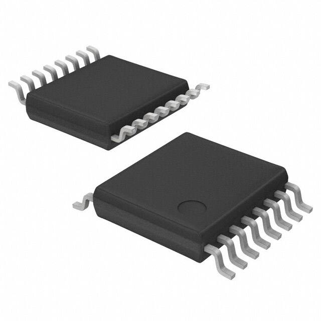
SSOP16
CASE 565AM
Functions and Features
MARKING DIAGRAM
• Achieves Linear Speed Control:
•
•
•
•
•
Applications can set the slope of the change in motor speed with
change in the input duty.
Minimized Speed Fluctuations in the Presence of Line or Load
Variations
Allows a Minimum Speed to be Set
Soft Start Function
Settings Using External Capacitors and Resistors
(to Support Easier Mass Production of End Products)
Supports both PWM Duty and Analog Voltage Control Inputs
LB8503
YMWL
LB8503
Y
M
WL
= Specific Device Code
= Year of Production
= Assembly Operation Month
= Wafer Lot Number
ORDERING INFORMATION
Device
Package
Shipping†
LB8503V−TLM−E
SSOP16
(Pb-Free)
2,000 /
Tape & Reel
LB8503V−W−AH
SSOP16
(Pb-Free/
Halogen Free)
2,000 /
Tape & Reel
†For information on tape and reel specifications,
including part orientation and tape sizes, please
refer to our Tape and Reel Packaging Specification
Brochure, BRD8011/D.
© Semiconductor Components Industries, LLC, 2017
April, 2019 − Rev. 3
1
Publication Order Number:
LB8503V/D
�LB8503V
SPECIFICATIONS
ABSOLUTE MAXIMUM RATINGS (TA = 25°C)
Parameter
Symbol
Supply Voltage
VCC max
Output Current
IO max
Conditions
Ratings
Unit
VCC pin
18
V
E0 pin
3
mA
FG Output Pin Output Voltage
VFG max
FGOUT pin
18
V
FG Output Pin Output Current
IFG max
FGOUT pin
10
mA
Allowable Power Dissipation
Pd max
When mounted on a circuit board
(Note 1)
0.8
W
Operating Temperature
Topr
−30 to +95
°C
Storage Temperature
Tstg
−55 to +150
°C
Stresses exceeding those listed in the Maximum Ratings table may damage the device. If any of these limits are exceeded, device functionality
should not be assumed, damage may occur and reliability may be affected.
1. Specified circuit board: 114.3 × 76.1 × 1.6mm3, glass epoxy.
RECOMMENDED OPERATING RANGE (TA = 25°C)
Parameter
Symbol
Conditions
Ratings
Unit
Supply Voltage Range 1
VCC1
VCC pin
7.5 to 17
V
Supply Voltage Range 2
VCC2
VCC pin, with VCC shorted to 6 VREG
5.5 to 6.5
V
2.5
mA
Output Current
IO
E0 pin
6 V Constant Voltage Output Current
IREG
−5
mA
CTL Pin Voltage
VCTL
0 to 6 VREG
V
LIM Pin Voltage
VLIM
0 to 6 VREG
V
VC1 Pin Voltage
VCI
0 to 6 VREG
V
Functional operation above the stresses listed in the Recommended Operating Ranges is not implied. Extended exposure to stresses beyond
the Recommended Operating Ranges limits may affect device reliability.
ELECTRICAL CHARACTERISTICS (TA = 25°C, VCC = 12 V)
Parameter
Supply Current
Symbol
Conditions
Min
ICC
Typ
Max
Unit
5.5
6.5
mA
6.0
6.0
6.2
6.1
V
6 V CONSTANT VOLTAGE OUTPUT (VREG PIN)
Output Voltage
VREG
LB8503−TLM−E
LB8503−W−AH
5.8
5.9
Line Regulation
DVREG1
VCC = 8 to 17 V
40
100
mV
Load Regulation
DVREG2
IO = −5 to 5 mA
10
100
mV
Temperature Coefficient
DVREG3
Design target (Note 2)
0
mV/°C
INTEGRATING AMPLIFIER BLOCK (E01)
Common-mode Input Voltage Range
VICM
2.0
High-level Output Voltage
VOH(E01)
IEO1 = −0.2 mA
Low-level Output Voltage
VOL(E01)
IEO1 = 0.2 mA
High-level Output Voltage
VOH(E03)
IEO1 = −0.2 mA
Low-level Output Voltage
VOL(E03)
IEO1 = 0.2 mA
VREG − 1.2
VREG
VREG − 0.8
0.8
V
V
1.0
V
INTEGRATING AMPLIFIER BLOCK (E03)
www.onsemi.com
2
VREG − 1.2
VREG − 0.8
0.8
V
1.0
V
�LB8503V
ELECTRICAL CHARACTERISTICS (TA = 25°C, VCC = 12 V) (continued)
Parameter
Symbol
Conditions
Min
Typ
Max
Unit
FGIN PIN
High-level Input Voltage
VFGH
3.0
VREG
V
Low-level Input Voltage
VFGL
0
1.5
V
Input Open Voltage
VFGO
VREG − 0.5
VREG
V
Hysteresis
VFGS
0.2
0.3
0.4
V
High-level Input Current
IFGH
VFGIN = 6 VREG
−10
0
10
mA
Low-level Input Current
IFGL
VFGIN = 0 V
−140
−110
mA
FGOUT PIN
Output Low Saturation Voltage
VFG
Output Leakage Current
IFGL
0.2
0.3
V
10
mA
RC PIN
VOH(RC)
3.2
3.45
3.7
V
Low-level Output Voltage
VOL(RC)
0.8
0.95
1.05
V
Clamp Voltage
VCLP(RC)
1.5
1.65
1.8
V
High-level Input Voltage
VCTH
2.0
VREG
V
Low-level Input Voltage
VCTL
0
1.0
V
Input Open Voltage
VCTO
VREG − 0.5
VREG
V
High-level Input Current
ICTH
VFGIN = 6 VREG
−10
0
10
mA
Low-level Input Current
ICTL
VFGIN = 0 V
−140
−110
mA
V
High-level Output Voltage
CTL PIN
C PIN
High-level Input Voltage
VOH(C)
VREG − 0.3
VREG − 0.1
Low-level Input Voltage
VOL(C)
1.8
2.0
IB(LIM)
VILIM
2.2
V
−1
1
mA
2.0
VREG
V
LIM PIN
Input Bias Current
Common-mode Input Voltage Range
SOFT PIN
Charge Current
Operation Voltage Range
IC(SOFT)
1.4
mA
VISOFT
2.0
VREG
V
IB(VCI)
−1
1
mA
VIVCI
2.0
VREG
V
VCI PIN
Input Bias Current
Common-mode Input Voltage Range
VCO PIN
High-level Output Voltage
VOH(VCO)
VREG − 0.2
V
Low-level Output Voltage
VOL(VCO)
2.0
V
Product parametric performance is indicated in the Electrical Characteristics for the listed test conditions, unless otherwise noted. Product
performance may not be indicated by the Electrical Characteristics if operated under different conditions.
2. The design specification items are design guarantees and are not measured.
www.onsemi.com
3
�LB8503V
Allowable Power Dissipation,
Pd max (W)
1.0
Specified circuit board:
114.3 × 76.1 × 1.6mm3,
glass epoxy board
0.8
0.6
0.4
0.35
0.2
0
−20
0
20
40
60
80
100
Ambient Temperature, TA (5C)
Figure 1. Pd max vs. TA
PIN ASSIGNMENT
EO3
EO1
EI
NC
16
15
14
13
GND FGOUT FGIN LIM
12
11
10
9
5
6
7
8
CVI
CVO
CTL
C
LB8503V
1
RC
2
3
4
SOFT VREG VCC
Figure 2. Pin Assignment (Top View)
PIN FUNCTION DESCRIPTION
Pin Name
Pin No.
Description
RC
1
One-shot multivibrator pulse width setting. Connect a resistor between this pin and VREG,
and a capacitor between this pin and ground.
SOFT
2
Soft start time setting. Connect a capacitor between this pin and VREG.
VREG
3
6 V regulator output. Connect a capacitor between this pin and ground for stabilization.
VCC
4
Power supply. Connect a capacitor between this pin and ground for stabilization.
CVI
5
Control voltage input
CVO
6
Duty pulse signal smoothed voltage output
CTL
7
Duty pulse signal input. The speed is controlled by the duty of this pulse signal.
C
8
Duty pulse signal smoothing. Connect a capacitor between this pin and VREG.
LIM
9
Minimum speed setting. Normally, the 6V regulator level is resistor divided to set this pin’s input level.
FGIN
10
FG pulse input
FGOUT
11
FG pulse output
GND
12
Grand pin
NC
13
NC pin
EI
14
One-shot multivibrator output and integrating amplifier input. A capacitor must be connected between
this pin and EO for this integration.
EO1
15
Integrating amplifier output. (For use with an accelerating driver IC if the command voltage becomes low
(single-phase systems).)
EO3
16
Integrating amplifier inverting output. (For use with an accelerating driver IC if the command voltage
becomes high (three-phase systems).)
www.onsemi.com
4
�LB8503V
BLOCK DIAGRAMS AND APPLICATION EXAMPLES
Combination with an accelerating driver IC when the command voltage goes low (single-phase systems).
Figure 3.
www.onsemi.com
5
�LB8503V
Combination with an accelerating driver IC when the command voltage goes high (three-phase systems).
Figure 4.
www.onsemi.com
6
�LB8503V
Speed Control Diagrams
The slope is determined by the external
constant connected to the RC pin.
(RPM)
For a larger RC
time constant
For a smaller RC
time constant
Speed
Minimum
speed
Determined by the LIM pin voltage
Low ← CTL pin (PWM DUTY)
High ← EO1 pin voltag e (V)
Low ←
EO3 pin voltag e (V)
0%
Set minimum
speed
→ High
→ Low
→ High
Variable speed
Low on duty
100%
Full speed
High on duty
CTL pin
6 VREG
LIM voltage
EO pin
EO1 voltage
0V
Figure 5.
Startup Timing (Soft Start)
V CC pin
CTL pin
Stop
Full speed
Soft start
The slope can be changed with the capacitor connected to
the C pin (A larger capacitor increases the slope.)
SOFT pin
Stop
Full speed
Figure 6.
www.onsemi.com
7
�LB8503V
Supplementary Operational Descriptions
The LB8503V accepts a duty pulse input and an FG signal
from the driver IC, and generates the driver IC control
voltage so that the FG period (motor speed) becomes
proportional to the control voltage.
LB8503V
Driver IC
FGIN
CTL
signal
FG
CTL
Closed
feedback
loop
EO
VTH
Figure 7.
The LB8503V then integrates that pulse waveform to
create the output driver IC control voltage (a DC voltage).
As shown in the figure below, the LB8503V generates
a pulse signal from edges on the FG signal and then
generates a pulse width waveform determined by the RC
time constant in a one-shot multivibrator.
FG
EDGE pulse
Slope due to the
RC time constant
RC pin
One-shot
Multivibrator
TRC(s) = 0.85RC
Figure 8.
Note, however, that since pulses determined by this RC
time constant are used, variation in the RC components will
appear as speed control errors.
It is also possible to change the slope of the VCTL/speed
relationship as shown in the speed control diagram in the
previous section by changing the pulse width with the RC
time constant.
www.onsemi.com
8
�LB8503V
Pin Setting Procedures
(Provided for Reference Purposes)
[RC Pin]
The slope in the speed control diagram is determined by
the RC pin time constant.
(RPM)
Motor
Full Speed
0%
CTL Duty (%)
100
Figure 9.
1. Determine the FG signal frequency (fFG (Hz)) at
the motor’s highest speed.
(When 2 FG pulses are created on each motor
revolution.)
f FG(Hz) +
2 rpm
60
the RC pin circuit.
Therefore, an appropriate resistor value can be
determined from either (eq. 3) or (eq. 4) below
from the result obtained in step above.
R+
(eq. 1)
2. Determine the time constant for the RC pin.
(Let DUTY be the control duty at the highest
motor speed. For example, 100% = 1.0,
60% = 0.6)
R
C+
3
DUTY
0.85 f FG
R+
R
C
0.01 mF
R
C
0.015 mF
(eq. 3)
(eq. 4)
Note that the temperature characteristics of the
curve are determined by the temperature
characteristics of the capacitor connected to the
RC pin.
A capacitor with excellent temperature
characteristics must be used to minimize motor
speed variation with temperature.
(eq. 2)
3. Determine the resistor and capacitor values.
The range of capacitors that can be used is from
0.01 to 0.015 mF due to the charge capabilities of
www.onsemi.com
9
�LB8503V
[CVO and CVI Pins]
These pins determine the origin of the slope. (To set the
origin to 0% at 0 rpm, short CVO to CVI.)
1. X axis shift (Resistor dividing the CVO to ground
potential).
(RPM)
Motor
Full Speed
X axis shift
0%
100%
CTL Duty (%)
Figure 10.
To shift the characteristics from a 0% = 0 rpm
origin to a situation where the speed at a duty of
30% is shifted to 0%:
First, determine the required CVI pin input voltage
at 0%.
CVI + 6 * (4
DUTY) + 6 * (4
+ 6 * 1.2 + 4.8 V
0.3)
CVO * CVI
CVI * ground
1.2 V
4.8 V
+ a ratio of 1:4
(eq. 6)
From the above, the desired resistor values will be
20 kW between CVO and CVI and 80 kW between
CVI and ground.
Note that the slope will change. (In this case, since
the resistor ratio is 1:4, the result will be 4/5 of
(or 0.8 times) the original slope.)
If required, the RC pin resistor value must be
changed to correct the slope.
(eq. 5)
Next, when CVO is 6 V, determine the resistor
values for the resistor divider between CVO and
ground such that the midpoint becomes 4.8 V.
LIM
VREF
SOFT
CVI
R4
+
CVO
R5
C
CTL
CTL
Figure 11.
www.onsemi.com
10
�LB8503V
2. Y axis shift
(Resistor dividing the CVO to VCC potential)
(RPM)
Motor
Full Speed
Y axis shift
0%
100%
CTL Duty (%)
Figure 12.
To shift the characteristics from a 0% = 0 rpm
origin to a situation where the speed is 0 rpm at
a duty of 30%:
First, determine the required CVO pin input
voltage at 0%.
CVO + 6 * (4
DUTY) + 6 * (4
0.25)
+6*1+5V
From the above, the desired resistor values will be
20 kW between CVO and CVI and 80 kW between
CVI and ground.
(Due to the current capability of the CVO pin, the
total resistor value must exceed 100 kW.)
Note that the slope will change. (In this case, since
the resistor ratio is 1:6, the result will be 6/7 of
(or 0.86 times) the original slope.)
If required, the RC pin resistor value must be
changed to correct the slope.
(eq. 7)
Determine the resistor values such that at
CVO = 5 V, CVI becomes 6 V.
CVO * CVI
CVI * V CC
+
1V
6V
+ a ratio of 1:6
(eq. 8)
VCC
LIM
VREF
SOFT
R4
CVI
CVO
C
CTL
CTL
Figure 13.
www.onsemi.com
11
�LB8503V
[LIM Pin]
The minimum speed is determined by the LIM pin
voltage.
(RPM)
Motor
Full Speed
10000
8000
6000
4000
Set Minimum
Speed
2000
0
0%
6V
100%
2V
CTL Duty (%)
CVO Pin Voltage (V)
Figure 14.
1. Determine the ratio of the required minimum
speed and the maximum speed.
Ra +
mininum speed
3. Determine the required LIM pin voltage:
LIM + 6 * (4
LIM + 6 * (4
In the example in the figure above:
Ra +
mininum speed
maximum speed
+
3000
+ 0.3
10000
+ 6 * (4
Ra
(eq. 11)
For example:
C a + maximum speed duty
+ 0.9
Ra
0.3 + 0.24
C a)
0.24) [ 5 V
(eq. 14)
4. Generate the LIM voltage by resistor dividing the
6 V regulator voltage.
For example, the resistor ratio to create a 5 V level
will be 1:5.
Thus the resistor values will be 10 kW between
6 VREG and LIM and 51 kW between LIM and
ground.
(eq. 10)
2. Determine the product of the duty that produces
the maximum speed and the value from
Equation 9.
C a + maximum speed duty
(eq. 13)
For example:
(eq. 9)
maximum speed
C a)
(eq. 12)
6 VREG
LIM
VREF
SOFT
CVI
Figure 15.
www.onsemi.com
12
�LB8503V
[C Pin]
Since a capacitor that can smooth the pin voltage is
connected to the C pin, if the CTL pin input signal frequency
is f (Hz), then the capacitor must meet the following
condition. (Here, R is the IC internal resistance of 180 W
(typical).)
1
+ t t RC
f
Note that the larger the capacitor, the slower its response
to changes in the input signal will be.
6 VREG
CTL pin input inverted
waveform (the frequency is the
same)
180 kW
CTL pin
(eq. 15)
A capacitor that can smooth the pin voltage is
connected here.
1/f = t < CR
C pin
VREF circuit
CTL circuit
Figure 16.
www.onsemi.com
13
�LB8503V
APPLICATION EXAMPLE 2
[Setting the Minimum Speed for an Origin of 0% = 0 rpm]
(RPM)
Motor
Full Speed
Set Minimum
Speed
0%
PWM Duty (%)
100%
Figure 17.
Figure 18.
When the speed control diagram origin is 0% = 0 rpm, the
CVO pin is connected to the CVI pin.
If the minimum speed is not set, connect the LIM pin to the
6 VREG pin.
www.onsemi.com
14
�LB8503V
APPLICATION EXAMPLE 3
[Origin Shift in the Y Direction (the Motor Turns at 0%)]
(RPM)
Motor
Full Speed
0%
PWM Duty (%)
100%
Figure 19.
Figure 20.
When the speed control diagram origin is set so the motor
turns at 0%, the CVO pin to ground potential difference is
resistor divided and the midpoint is input to the CVI pin.
The speed at 0% can be changed with the resistor ratio.
www.onsemi.com
15
�LB8503V
APPLICATION EXAMPLE 4
[Origin Shift in the X Axis Direction (The Motor Turns at a Duty of 10% or Higher) Plus a Minimum Speed Setting]
(RPM)
Motor
Full Speed
0%
PWM Duty (%)
100%
Figure 21.
Figure 22.
The duty at which rotation starts can be changed by
changing the resistor ratio.
Note that the total value of the resistors R4 and R5 must
exceed 100 kW.
When the origin in the speed control diagram is set so that
the motor starts turning when the duty is above 0%. the
potential difference between the CVO pin and VCC is
resistor divided, and that divided level is input to the CVI
pin.
www.onsemi.com
16
�LB8503V
APPLICATION EXAMPLE 5
[DC Voltage Speed Control]
(RPM)
Motor
Full Speed
Set Minimum
Speed
0
6V
CV1 Pin Voltage (V)
2V
Figure 23.
Figure 24.
When the motor speed is controlled by a DC voltage, than
voltage must be in the range from 2 V to 6 VREG.
Note that the motor stops when the control voltage is at
6 VREG, and the motor speed increases as the voltage falls.
www.onsemi.com
17
�LB8503V
APPLICATION EXAMPLE 6
[Fixed Speed + Soft Start]
(RPM)
Motor
Full Speed
0%
6V
20%
40%
60%
80%
CTL Signal (PWM Duty)
C Pin Voltage
100%
Figure 25.
Figure 26.
With this circuit, the motor speed remains constant even
if there are fluctuations in the supply voltage or static
voltage. It is also possible to input a fixed-duty signal to the
CTL pin signal input as an input signal for which soft start
is enabled at startup.
www.onsemi.com
18
�LB8503V
APPLICATION EXAMPLE 7
[Used in Combination with the LB11660FV]
Figure 27.
In this circuit, the dynamic range of the LB8503V EO pin
(the range from the amplifier block output high to output low
levels) must be wider than the dynamic range (from the high
to low levels of the PWM signal) of VTH pin of driver IC
with which this IC is combined.
However, since the LB11660FV PWM low-level voltage
is lower than the LB8503V amplifier output low-level
voltage, it must be resistor divided.
www.onsemi.com
19
�MECHANICAL CASE OUTLINE
PACKAGE DIMENSIONS
SSOP16 (225mil)
CASE 565AM
ISSUE A
GENERIC
MARKING DIAGRAM*
SOLDERING FOOTPRINT*
5.80
(Unit: mm)
1.0
0.32
0.65
NOTE: The measurements are not to guarantee but for reference only.
*For additional information on our Pb−Free strategy and soldering
details, please download the ON Semiconductor Soldering and
Mounting Techniques Reference Manual, SOLDERRM/D.
DOCUMENT NUMBER:
DESCRIPTION:
DATE 23 OCT 2013
98AON66065E
SSOP16 (225MIL)
XXXXXXXXXX
YMDDD
XXXXX = Specific Device Code
Y = Year
M = Month
DDD = Additional Traceability Data
*This information is generic. Please refer to
device data sheet for actual part marking.
Pb−Free indicator, “G” or microdot “ G”,
may or may not be present.
Electronic versions are uncontrolled except when accessed directly from the Document Repository.
Printed versions are uncontrolled except when stamped “CONTROLLED COPY” in red.
PAGE 1 OF 1
ON Semiconductor and
are trademarks of Semiconductor Components Industries, LLC dba ON Semiconductor or its subsidiaries in the United States and/or other countries.
ON Semiconductor reserves the right to make changes without further notice to any products herein. ON Semiconductor makes no warranty, representation or guarantee regarding
the suitability of its products for any particular purpose, nor does ON Semiconductor assume any liability arising out of the application or use of any product or circuit, and specifically
disclaims any and all liability, including without limitation special, consequential or incidental damages. ON Semiconductor does not convey any license under its patent rights nor the
rights of others.
© Semiconductor Components Industries, LLC, 2019
www.onsemi.com
�ON Semiconductor and
are trademarks of Semiconductor Components Industries, LLC dba ON Semiconductor or its subsidiaries in the United States and/or other countries.
ON Semiconductor owns the rights to a number of patents, trademarks, copyrights, trade secrets, and other intellectual property. A listing of ON Semiconductor’s product/patent
coverage may be accessed at www.onsemi.com/site/pdf/Patent−Marking.pdf. ON Semiconductor reserves the right to make changes without further notice to any products herein.
ON Semiconductor makes no warranty, representation or guarantee regarding the suitability of its products for any particular purpose, nor does ON Semiconductor assume any liability
arising out of the application or use of any product or circuit, and specifically disclaims any and all liability, including without limitation special, consequential or incidental damages.
Buyer is responsible for its products and applications using ON Semiconductor products, including compliance with all laws, regulations and safety requirements or standards,
regardless of any support or applications information provided by ON Semiconductor. “Typical” parameters which may be provided in ON Semiconductor data sheets and/or
specifications can and do vary in different applications and actual performance may vary over time. All operating parameters, including “Typicals” must be validated for each customer
application by customer’s technical experts. ON Semiconductor does not convey any license under its patent rights nor the rights of others. ON Semiconductor products are not
designed, intended, or authorized for use as a critical component in life support systems or any FDA Class 3 medical devices or medical devices with a same or similar classification
in a foreign jurisdiction or any devices intended for implantation in the human body. Should Buyer purchase or use ON Semiconductor products for any such unintended or unauthorized
application, Buyer shall indemnify and hold ON Semiconductor and its officers, employees, subsidiaries, affiliates, and distributors harmless against all claims, costs, damages, and
expenses, and reasonable attorney fees arising out of, directly or indirectly, any claim of personal injury or death associated with such unintended or unauthorized use, even if such
claim alleges that ON Semiconductor was negligent regarding the design or manufacture of the part. ON Semiconductor is an Equal Opportunity/Affirmative Action Employer. This
literature is subject to all applicable copyright laws and is not for resale in any manner.
PUBLICATION ORDERING INFORMATION
LITERATURE FULFILLMENT:
Email Requests to: orderlit@onsemi.com
ON Semiconductor Website: www.onsemi.com
◊
TECHNICAL SUPPORT
North American Technical Support:
Voice Mail: 1 800−282−9855 Toll Free USA/Canada
Phone: 011 421 33 790 2910
www.onsemi.com
1
Europe, Middle East and Africa Technical Support:
Phone: 00421 33 790 2910
For additional information, please contact your local Sales Representative
�