Battery Protection IC for
1-Cell Lithium-Ion with
Integrated Power MOSFET
LC05111CMT�
Overview
The LC05111CMT is a protection IC for 1−cell lithium−ion
secondary batteries with integrated power MOSFET. Also it integrates
highly accurate detection circuits and detection delay circuits to
prevent batteries from over−charging, over−discharging, over−current
discharging and over−current charging.
A battery protection system can be made by only LC05111CMT and
few external parts.
Features
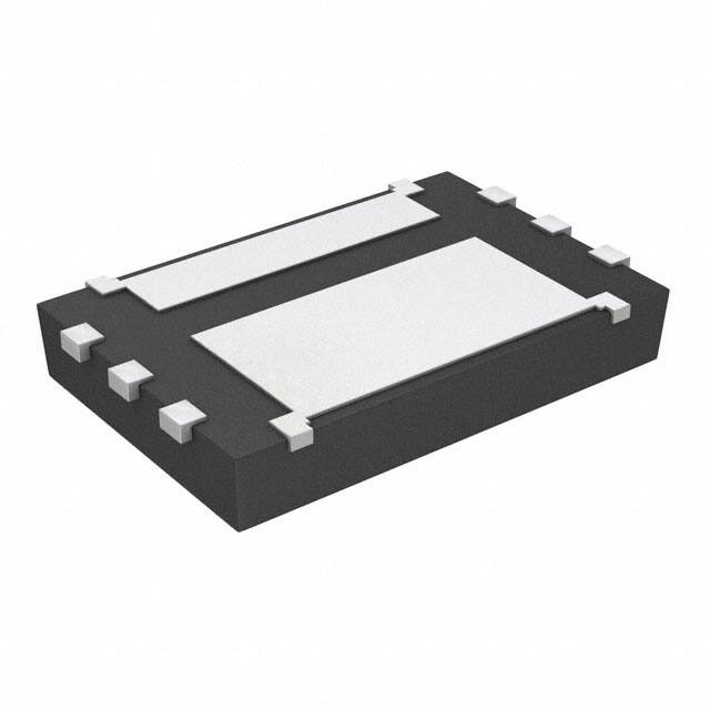
www.onsemi.com
WDFN6 2.6x4.0, 0.65P,
DUAL FLAG
CASE 511BZ
• Charge−and−discharge Power MOSFET are Integrated at
•
•
•
•
•
•
•
•
•
•
•
•
Ta = 25_C, VCC = 4.5 V
♦ ON Resistance (total of charge and discharge) 11.2 mW (typ)
Highly Accurate Detection Voltage/Current at Ta = 25°C, VCC = 3.7 V
♦ Over−charge Detection
±25 mV
♦ Over−discharge Detection
±50 mV
♦ Charge Over−current Detection
±0.7 A
♦ Discharge Over−current Detection ±0.7 A
Delay Time for Detection and Release (fixed internally)
Discharge/Charge Over−current Detection is Compensated for
Temperature Dependency of Power FET
0 V Battery Charging
: “Permission”
Auto Wake−up Function Battery Charging: “Permission”
Over Charge Detection Voltage
: 4.0 V to 4.5 V (5 mV steps)
Over Charge Release Hysteresis
: 0 V to 0.3 V (100 mV steps)
Over Discharge Detection Voltage : 2.2 V to 2.7 V (50 mV steps)
Over Discharge Release Hysteresis at Auto Wake−up : 0 V to 0.6 V
(200 mV steps)
Over Discharge Release Hysteresis : 0 V to 0.075 V (25 mV steps)
Discharge Over Current Detection : 2.0 A to 8.0 A (0.5 A steps)
Charge Over Current Detection
: −8.0 A to −2.0 A (0.5 A steps)
MARKING DIAGRAM
XXXXX
AYWWG
XXXXX
A
Y
WW
G
= Specific Device Code
= Assembly Location
= Year
= Work Week
= Pb−Free Package
(Note: Microdot may be in either location)
*This information is generic. Please refer to
device data sheet for actual part marking.
ORDERING INFORMATION
See detailed ordering and shipping information on page 15 of
this data sheet.
Typical Applications
• Lithium Ion Battery Protection
© Semiconductor Components Industries, LLC, 2017
September, 2019 − Rev. 13
1
Publication Order Number:
LC05111CMT/D
�LC05111CMT
Specifications
Table 1. ABSOLUTE MAXIMUM RATINGS TA = 25°C (Notes 1 and 2)
Parameter
Symbol
Ratings
Unit
Conditions
Supply voltage
VCC
−0.3 to +12.0
V
Between PAC+ and VCC : R1 = 680 W
S1 − S2 voltage
VS1−S2
24.0
V
CS terminal Input voltage
CS
VCC−24.0
V
Charge or discharge current
BAT−, PAC−
10.0
A
TST Input voltage
TST
−0.3 to +7.0
V
Storage temperature
Tstg
−55 to +125
°C
Current between S1 and S2(DC)
ID
10.0
A
VCC = 3.7 V
Current between S1 and S2
(continuous pulse)
IDP
35
A
Pulse Width < 10 ms, duty cycle < 1%
Operating ambient temperature
Topr
−40 to +85
°C
Allowable power dissipation
Pd
450
mW
Junction temperature
Tj
125
°C
Glass epoxy four−layer board. Board
size 27.4 mm x 3.1 mm x 0.8 mm
Stresses exceeding those listed in the Maximum Ratings table may damage the device. If any of these limits are exceeded, device functionality
should not be assumed, damage may occur and reliability may be affected.
1. Absolute maximum ratings represent the values which cannot be exceeded at any given time.
2. If you intend to use this IC continuously under high temperature, high current, high voltage, or drastic temperature change, even if it used
within the range of absolute maximum ratings or operating conditions, there is a possibility of decrease reliability. Please contact us for
confirmation.
PAC+
R1
VCC
Controller IC
C1
Battery
TST
VSS
S2
S1
CS
R2
PAC−
Figure 1. Example of Application Circuit
Table 2.
Components
Recommended Value
Max
Unit
R1
680
1k
W
R2
1k
2k
W
C1
0.1 m
1.0 m
F
Description
3. We don’t guarantee the characteristics of the circuit shown above.
4. TST pin would be better to be connected to VSS pin, though it is connected to VSS with internal resistor (100 kW typ).
5. Battery voltage drop occurs, a current of about 60 mA flow period of 1.5 V − 1.3 V.
www.onsemi.com
2
�LC05111CMT
Table 3. ELECTRICAL CHARACTERISTICS
Parameter
Symbol
Conditions
Min
Typ
Max
Unit
25°C
Vov_set −25
Vov_set
Vov_set +25
mV
−30 to 70°C
Vov_set −30
Vov_set
Vov_set +30
DETECTION VOLTAGE
Over−charge detection voltage
Vov
Over−charge release voltage
Vovr
Over−discharge detection
voltage
Vuv
Over−discharge release
voltage
Vuvr
Over−discharge release
voltage2
Vuvr2
Discharge over−current
detection current
Ioc
Discharge over−current
release current
Iocr
R1=680W
R1=680W
R1=680W
R1=680W
CS=0V
R1=680W
CS=open
R2=1kW
R2=1kW
25°C
Vovr_set −40
Vovr_set
Vovr_set +40
−30 to 70°C
Vovr_set −70
Vovr_set
Vovr_set +70
25°C
Vuv_set −50
Vuv_set
Vuv_set +50
−30 to 70°C
Vuv_set −80
Vuv_set
Vuv_set +80
25°C
Vuvr_set −100
Vuvr_set
Vuvr_set +100
−30 to 70°C
Vuvr_set −120
Vuvr_set
Vuvr_set +120
25°C
Vuvr2_set −100
Vuvr2_set
Vuvr2_set +100
−30 to 70°C
Vuvr2_set −120
Vuvr2_set
Vuvr2_set +120
25°C
VCC=3.7V
Ioc_set −0.7
Ioc_set
Ioc_set +0.7
−30 to 70°C
VCC=2.6 to 4.3V
Ioc_set −1.2
Ioc_set
Ioc_set +1.2
25°C
VCC=3.7V
(Ioc_set−0.7)
(Ioc_set)
(Ioc_set+0.7)
−30 to 70°C
VCC=2.6 to 4.3V
(Ioc_set−1.2)
(Ioc_set)
oc_set+1.2)
mV
mV
mV
mV
A
A
Discharge over−current detection current(Short circuit)
Ioc2
R2=1kW
25°C
VCC=3.7V
Ioc2_set*0.8
Ioc2_set
Ioc2_set*1.2
A
Charge over−current detection current
Ioch
R2=1kW
25°C
VCC=3.7V
Ioch_set −0.7
Ioch_set
Ioch_set +0.7
A
−30 to 70°C
VCC=2.6 to 4.3V
Ioch_set −1.2
Ioch_set
Ioch_set +1.2
25°C
VCC=3.7V
Ioch_set −0.7
Ioch_set
Ioch_set +0.7
−30 to 70°C
VCC=2.6 to 4.3V
Ioch_set −1.2
Ioch_set
Ioch_set +1.2
Charge over−current release current
Iochr
R2=1kW
A
INPUT VOLTAGE
Vchg
VCC−CS
VCC−GND=0V
25°C
Operating current
Icc
At normal
state
25°C
VCC=3.7V
Stand−by current
Istb
At Stand−by
state
Auto wake−up
= enable
25°C
VCC=2.0V
ON resistance 1 of integrated power MOSFET
Ron1
VCC=3.1V
I=±2.0A
25°C
10.4
ON resistance 2 of integrated power MOSFET
Ron2
VCC=3.7V
I=±2.0A
25°C
ON resistance 3 of integrated power MOSFET
Ron3
VCC=4.0V
I=±2.0A
ON resistance 4 of integrated power MOSFET
Ron4
VCC=4.5V
I=±2.0A
Operating Voltage for 0V
charging
1.4
V
6
mA
0.95
mA
13
18.2
mW
9.6
12
15.6
mW
25°C
9.2
11.6
15
mW
25°C
8.8
11.2
14
mW
CURRENT CONSUMPTION
3
RESISTANCE
www.onsemi.com
3
�LC05111CMT
Table 3. ELECTRICAL CHARACTERISTICS
Parameter
Symbol
Conditions
Min
Typ
Max
Unit
RESISTANCE
Internal resistance
(VCC−CS)
Rcsu
VCC=Vuv_set
CS=0V
25°C
300
kW
Internal resistance
(VSS−CS)
Rcsd
VCC=3.7V
CS=0.1V
25°C
15
kW
DETECTION AND RELEASE DELAY TIME
Over−charge detection delay time
Tov
Over−charge release delay
time
Tovr
Over−discharge detection
delay time
Tuv
Over−discharge release delay time
Tuvr
Discharge over−current
detection delay time 1
Toc1
Discharge over−current
release delay time 1
Tocr1
VCC=3.7V
Discharge over−current
detection delay time 2
(Short circuit)
Toc2
VCC=3.7V
Charge Over−current
detection delay time
Toch
Charge Over−current
release delay time
Tochr
VCC=3.7V
VCC=3.7V
VCC=3.7V
25°C
0.8
1
1.2
−30 to 70°C
0.6
1
1.5
25°C
12.8
16
19.2
−30 to 70°C
9.6
16
24
25°C
16
20
24
−30 to 70°C
12
20
30
25°C
0.9
1.1
1.3
−30 to 70°C
0.6
1.1
1.5
25°C
9.6
12
14.4
−30 to 70°C
7.2
12
18
25°C
3.2
4
4.8
−30 to 70°C
2.4
4
6
25°C
280
400
560
−30 to 70°C
180
400
800
25°C
12.8
16
19.2
−30 to 70°C
9.6
16
24
25°C
3.2
4
4.8
−30 to 70°C
2.4
4
6
sec
ms
ms
ms
ms
ms
ms
ms
ms
Product parametric performance is indicated in the Electrical Characteristics for the listed test conditions, unless otherwise noted. Product
performance may not be indicated by the Electrical Characteristics if operated under different conditions.
www.onsemi.com
4
�LC05111CMT
Table 4. SELECTION GUIDE
Device
Vov(V)
Vovr(V)
Vuv(V)
Vuvr(V)
Vuvr2(V)
AWUP
Ioc(A)
Ioch(A)
Ioc2(A)
0Vcharge
LC05111C01MTTTG
4.425
4.225
2.500
2.500
2.900
enable
6.0
4.0
17.5
enable
LC05111C02MTTTG
4.280
4.180
2.700
2.700
2.900
enable
6.0
3.5
21.5
enable
LC05111C05MTTTG
4.425
4.225
2.300
2.300
2.700
enable
4.0
4.0
17.5
enable
LC05111C13MTTTG
4.240
4.140
2.700
2.700
2.900
enable
3.0
2.5
15.0
enable
LC05111C14MTTTG
4.445
4.245
2.600
2.600
3.000
enable
4.0
4.0
17.5
enable
LC05111C16MTTTG
4.470
4.270
2.500
2.500
2.900
enable
7.0
5.7
17.5
enable
LC05111C18MTTTG
4.200
4.000
2.700
2.750
2.900
enable
6.0
2.5
17.5
enable
LC05111C20MTTTG
4.310
4.110
2.500
2.500
2.900
enable
3.0
2.0
15.0
enable
LC05111C21MTTTG
4.240
4.140
2.700
2.700
2.900
enable
6.0
5.0
17.5
enable
LC05111C23MTTTG
4.425
4.225
2.600
2.600
3.000
enable
5.2
4.0
17.5
enable
LC05111C25MTTTG
4.225
4.025
2.600
2.600
3.000
enable
4.2
4.2
17.5
enable
Pdmax−Ta Graph
www.onsemi.com
5
�LC05111CMT
Recommended Board Layout
PAC+
BAT+
R1
Battery
C1
VCC
Controller IC
TST
VSS
C2
(option)
S1
S2
CS
R2
PAC−
BAT−
C3
(option)
Figure 2. Board Schematic
All layer
27.4mm
3.1mm
Top layer
2nd layer
3rd layer
4th layer
Figure 3. Board size L = 27.4 mm W = 3.1 mm H = 0.8 mm glass−epoxy 4 layers
www.onsemi.com
6
�LC05111CMT
NOTES:
1.Please connect the VSS line to a pin of S1 directly.
2.Please connect the resistance of R2 to a pin of S2 directly.
It can perform the detection of the overcurrent exactly by
performing these.
It can get rid of influence of the wiring impedance caused by
a severe electric current flowing through S1 and S2.
Red line of schematic is very important line.
Zoom
1
2
Figure 4. All
www.onsemi.com
7
�LC05111CMT
Table 5. PIN FUNCTIONS
Pin No.
Symbol
1
S2
Charger minus voltage input pin
Pin Function
2
CS
Charger minus voltage input pin
3
TST
Package trimming Terminal
4
VSS
Negative power Input
5
VCC
VCC terminal
Description
Connected to GND by internal 100 kW resistor
6
S1
7
Drain
Negative power input
Drain of FET
Exposed pad
8
Sub
IC Sub (VSS)
Exposed pad
TST
VCC
Power
Control
OSC
Control Circuit
Over−discharge
Detector
Discharge
Over−current
Detector
Level
Shifter
1.2V
Short−circuit
Detector
1.2 V
Over−charge
Detector
Charge
Over−current
Detector
DCHG_SW
VSS
S1
Figure 5. Block Diagram
www.onsemi.com
8
CHG_SW
S2 CS
(Pack minus)
�LC05111CMT
Description of Operation
(1) Normal mode
• LC05111CMT controls charging and discharging by
detecting cell voltage (VCC) and controls S2−S1
current. In case that cell voltage is between
over−discharge detection voltage (Vuv) and
over−charge detection voltage (Vov), and S2−S1 current
is between charge over−current detection current (Ioch)
and discharge over−current detection current (Ioc),
internal power MOS FETs as CHG_SW, DCHG_SW
are all turned ON.
This is the normal mode, and it is possible to be
charged and discharged.
(3) Over−discharging mode
• If cell voltage will get lower than over−discharge
•
(2) Over−charging mode
• Internal power MOS FET as CHG_SW will be turned
off if cell voltage will get equal to or higher than
over−charge detection voltage (Vov) over the delay
time of over−charging (Tov).
This is the over−charging detection mode.
• The recovery from over−charging will be made after
the following three conditions are all satisfied.
detection voltage (Vuv) over the delay time of over−
discharging (Tuv), discharging will be shut off, because
internal power FETs as DCHG_SW is turned off.
This is the over−discharging mode.
After detecting over−discharging, CS pin will be pulled
up to Vcc by internal resistor Rcsu and the bias of
internal circuits will be shut off. (Stand−by mode)
In stand−by mode, operating current is suppressed
under 0.95 mA (max).
The recovery from stand−by mode will be made by
internal circuits biased after the following two
conditions are satisfied.
a.
b.
•
a.
b.
Charger is removed from IC.
Cell voltage will get lower than over−charge
release voltage (Vovr) over the delay time of
over−charging release (Tovr) due to discharging
through load.
Consequently, internal power MOS FET as CHG_SW will
be turned on and normal mode will be resumed.
• In over−charging mode, discharging over−current
detection is made only when CS pin will get higher
than discharging over−current detection current 2(Ioc2),
because discharge current flows through parasitic diode
of CHG_SW FET.
If CS pin voltage will get higher than discharging
over−current detection current 2 (Ioc2) over the delay
time of discharging over−current 2 (Toc2), discharging
will be shut off, because internal power FETs as
DCHG_SW is turned off.(short−circuit detection mode)
After detecting short−circuit, CS pin will be pulled
down to Vss by internal resistor Rcsd.
Charger is connected.
VCC level rise more than Over−discharge
release voltage2(Vuvr2) without charger.(Auto
wake−up function)
If CS pin voltage will get lower than charger detecting
voltage (Vchg) by connecting charger under the
condition that cell voltage is lower than over−discharge
detection voltage, internal power MOS FET as
DCHG_SW is turned on and power dissipation in
power MOS FETs is suppressed.
*In case that charging current is low enough, ripple current
will be appeared at S2 terminal when CS pin voltage is near
by the threshold of charger detecting voltage (Vchg).
It is caused that the two modes, charger detected and charger
not detected (charging through parasitic diodes of
DCHG_SW, is alternately appeared.
• By continuing to be charged, if cell voltage will get
higher than over−discharge detection voltage (Vuvr)
over the delay time of over−discharging (Tuvr), internal
power MOS FETs as DCHG_SW is turned on and
normal mode will be resumed.
• In over−discharge detection mode, charging
over−current detection does not operate.
By continuing to be charged, charging over−current
detection starts to operate after cell voltage goes up
more than over−discharge release voltage (Vuvr).
The recovery from short circuit detection in over−charging
mode will be made after the following two conditions are
satisfied.
a.
Load is removed from IC.
b.
CS pin voltage will get equal to or lower than
discharging over−current detection current 2
(Ioc2) due to CS pin pulled down through Rcsd.
Consequently, internal power MOS FET as DCHG_SW will
be turned on, and over−charging detection mode will be
resumed.
(4) Discharging over−current detection mode 1
• Internal power MOS FET as DCHG_SW will be turned
off and discharging current will be shut off if CS pin
voltage will get equal to or higher than discharging
over−current detection current (Ioc) over the delay time
of discharging over−current (Toc1).
This is the discharging over−current detection mode 1.
In discharging over−current detection mode 1, CS pin
will be pulled down to Vss with internal resistor Rcsd.
• The recovery from discharging over−current detection
mode will be made after the following two conditions
are satisfied.
www.onsemi.com
9
�LC05111CMT
• The recovery from charging over−current detection
a.
b.
Load is removed from IC.
CS pin voltage will get equal to or lower than
discharging over−current release current (Iocr)
over the delay time of discharging over−current
release (Tocr1) due to CS pin pulled down
through Rcsd.
Consequently, internal power MOS FET as DCHG_SW will
be turned on, and normal mode will be resumed.
(5) Discharging over−current detection mode 2 (short circuit
detection)
• Internal power MOS FET as DCHG_SW will be turned
off and discharging current will be shut off if CS pin
voltage will get equal to or higher than discharging
over−current detection current2 (Ioc2) over the delay
time of discharging over−current 2 (Toc2).
This is the short circuit detection mode.
• In short circuit detection mode, CS pin will be pulled
down to Vss by internal resistor Rcsd.
The recovery from short circuit detection mode will be
made after the following two conditions are satisfied.
mode will be made after the following two conditions is
satisfied.
a.
Charger is removed from IC and CS pin will
get higher by load connected.
b.
CS pin voltage will get equal to or higher than
charging over−current release current (Iochr)
over the delay time of charging over−current
release (Tocrh).
Consequently, internal power MOS FET as CHG_SW will
be turned on, and normal mode will be resumed.
*Internal current flows out through CS and S2 terminals.
After charger is removed, it flows through parasitic diode of
CHG_SW FET.
Therefore, CS pin voltage will go up more than charging
over−current release current (Iochr).
So CS pin voltage is not an indispensable condition for
recovery from charging over−current detection.
(7) Available Voltage for 0 V charging
It is the function that the voltage of a connected battery can
charge from the state that became 0 V by self−discharge. The
0 V battery charge start battery charger voltage (Vchg), it fix
a gate of the charge system order FET to the VDD terminal
voltage when it connect a battery charger of the
above−mentioned voltage to PAC+ terminal between PAC−
terminals.
Gate−source voltage of the charge control FET becomes
equal to the turn−on voltage or more due to the charger
voltage, the charging control FET.
To start charging row is turned on.
Discharge control FET is off at this time, the charge current
flows through the internal parasitic diode in the discharging
control FET. It is the normal state battery voltage becomes
the overdischarge release voltage (Vuvr) or more.
a.
b.
Load is removed from IC.
CS pin voltage will get equal to or lower than
discharging over−current release current (Iocr)
over the delay time of discharging over−current
release (Tocr1) due to CS pin pulled down
through Rcsd.
Consequently, internal power MOS FET as DCHG_SW will
be turned on, and normal mode will be resumed.
(6) Charging over−current detection mode
• Internal power MOS FET as CHG_SW will be turned
off and charging current will be shut off if CS pin
voltage will get equal to or lower than charging
over−current detection current (Ioch) over the delay
time of charging over−current (Toch).
This is the charging over−current detection mode.
www.onsemi.com
10
�LC05111CMT
Timing Charts
Charger
connection
Load
connection
Charger
connection
VCC
Vov
Vovr
Vuv/Vuvr
DCHG _SW
VCC
S1
CHG _SW
VCC
S2
CS
VCC
S1
Tov
Tovr
Tuv
Tuvr
Figure 6. Over−charged detection/release, Over−discharge detection/release
(Connect charger)
www.onsemi.com
11
�LC05111CMT
Charger connection
Load
connection
Load connection
VCC
Vov
Vovr
Vuvr 2
Vuv
DCHG _SW
VCC
S1
CHG _SW
VCC
S2
CS
VCC
S1
Tov
Tovr
Tuv
Figure 7. Over−charge detection/release, Over−discharged detection/release
(Non−connect charger)
www.onsemi.com
12
Tuvr
�LC05111CMT
Load connection
Load connection
VCC
Vov
Vuv
DCHG _SW
VCC
S1
CHG _SW
VCC
S2
CS
VCC
Voc 2
S1
Discharge
Current
Ioc
Toc 1
Toc 2
Tocr 1
Tocr 1
Figure 8. Discharge over−current detection1, Discharge over−current detection2
(Short circuit)
www.onsemi.com
13
�LC05111CMT
Charger
connection
Load connection
VCC
Vov
Vuv
DCHG _SW
VCC
S1
CHG _SW
VCC
S2
CS
VCC
S1
Charge /Discharge
Current
0
Ioch
Toch
Tochr
Figure 9. Charge Over−current Detection
www.onsemi.com
14
�LC05111CMT
Table 6. ORDERING INFORMATION
Device
Package
Shipping (Qty / Packing)
LC05111C01MTTTG
WDFN6 2.6x4.0, 0.65P, Dual Flag
(Pb−Free / Halogen Free)
4000 / Tape & Reel
LC05111C02MTTTG
WDFN6 2.6x4.0, 0.65P, Dual Flag
(Pb−Free / Halogen Free)
4000 / Tape & Reel
LC05111C05MTTTG
WDFN6 2.6x4.0, 0.65P, Dual Flag
(Pb−Free / Halogen Free)
4000 / Tape & Reel
LC05111C13MTTTG
WDFN6 2.6x4.0, 0.65P, Dual Flag
(Pb−Free / Halogen Free)
4000 / Tape & Reel
LC05111C14MTTTG
WDFN6 2.6x4.0, 0.65P, Dual Flag
(Pb−Free / Halogen Free)
4000 / Tape & Reel
LC05111C16MTTTG
WDFN6 2.6x4.0, 0.65P, Dual Flag
(Pb−Free / Halogen Free)
4000 / Tape & Reel
LC05111C18MTTTG
WDFN6 2.6x4.0, 0.65P, Dual Flag
(Pb−Free / Halogen Free)
4000 / Tape & Reel
LC05111C20MTTTG
WDFN6 2.6x4.0, 0.65P, Dual Flag
(Pb−Free / Halogen Free)
4000 / Tape & Reel
LC05111C21MTTTG
WDFN6 2.6x4.0, 0.65P, Dual Flag
(Pb−Free / Halogen Free)
4000 / Tape & Reel
LC05111C23MTTTG
WDFN6 2.6x4.0, 0.65P, Dual Flag
(Pb−Free / Halogen Free)
4000 / Tape & Reel
LC05111C25MTTTG
WDFN6 2.6x4.0, 0.65P, Dual Flag
(Pb−Free / Halogen Free)
4000 / Tape & Reel
www.onsemi.com
15
�MECHANICAL CASE OUTLINE
PACKAGE DIMENSIONS
WDFN6 2.6x4.0, 0.65P, Dual Flag
CASE 511BZ
ISSUE B
1
SCALE 2:1
A B
D
5 4
6
PIN ONE
REFERENCE
2X
0.10 C
2X
0.10 C
ÉÉ
ÉÉ
ÉÉ
1
2 3
TOP VIEW
A
0.05 C
A3
SIDE VIEW
NOTE 3
D2
4X
L3
1
3
SEATING
PLANE
XXXXX
XXXXX
AYWWG
G
w/o ejector pin
L2
b2
6
4
6X
e
BOTTOM VIEW
b
0.10
M
C A B
0.05
M
C
XXXXX
AYWWG
w/ ejector pin
XXXXX = Specific Device Code
A
= Assembly Location
Y
= Year
WW
= Work Week
G
= Pb−Free Package
(Note: Microdot may be in either location)
*This information is generic. Please refer to
device data sheet for actual part marking.
E2
L
MILLIMETERS
MIN
MAX
−−−
0.80
0.10
0.25
0.25
0.40
0.15
0.30
2.60 BSC
2.075
2.375
1.20
1.50
0.40
0.70
4.00 BSC
3.80 REF
2.95
3.05
2.25
2.55
0.65 BSC
0.12
0.32
−−−
0.10
−−−
0.55
GENERIC
MARKING DIAGRAM*
4X
E3
6X
C
D4
D3
4X
DIM
A
A3
b
b2
D
D2
D3
D4
E
E1
E2
E3
e
L
L2
L3
E1 E
0.10 C
8X
DATE 02 NOV 2016
NOTES:
1. DIMENSIONING AND TOLERANCING PER
ASME Y14.5M, 1994.
2. CONTROLLING DIMENSION: MILLIMETERS.
3. PROFILE TOLERANCE APPLIES TO THE
EXPOSED PADS AS WELL AS THE LEADS.
RECOMMENDED
SOLDERING FOOTPRINT*
2.29
0.53
0.27
6X
0.40
2.50
4.20
PACKAGE
OUTLINE
1
0.65
PITCH
6X
0.40
DIMENSION: MILLIMETERS
*For additional information on our Pb−Free strategy and soldering
details, please download the ON Semiconductor Soldering and
Mounting Techniques Reference Manual, SOLDERRM/D.
DOCUMENT NUMBER:
DESCRIPTION:
98AON81958F
Electronic versions are uncontrolled except when accessed directly from the Document Repository.
Printed versions are uncontrolled except when stamped “CONTROLLED COPY” in red.
WDFN6 2.6X4.0, 0.65P, DUAL FLAG
PAGE 1 OF 1
ON Semiconductor and
are trademarks of Semiconductor Components Industries, LLC dba ON Semiconductor or its subsidiaries in the United States and/or other countries.
ON Semiconductor reserves the right to make changes without further notice to any products herein. ON Semiconductor makes no warranty, representation or guarantee regarding
the suitability of its products for any particular purpose, nor does ON Semiconductor assume any liability arising out of the application or use of any product or circuit, and specifically
disclaims any and all liability, including without limitation special, consequential or incidental damages. ON Semiconductor does not convey any license under its patent rights nor the
rights of others.
© Semiconductor Components Industries, LLC, 2019
www.onsemi.com
�ON Semiconductor and
are trademarks of Semiconductor Components Industries, LLC dba ON Semiconductor or its subsidiaries in the United States and/or other countries.
ON Semiconductor owns the rights to a number of patents, trademarks, copyrights, trade secrets, and other intellectual property. A listing of ON Semiconductor’s product/patent
coverage may be accessed at www.onsemi.com/site/pdf/Patent−Marking.pdf. ON Semiconductor reserves the right to make changes without further notice to any products herein.
ON Semiconductor makes no warranty, representation or guarantee regarding the suitability of its products for any particular purpose, nor does ON Semiconductor assume any liability
arising out of the application or use of any product or circuit, and specifically disclaims any and all liability, including without limitation special, consequential or incidental damages.
Buyer is responsible for its products and applications using ON Semiconductor products, including compliance with all laws, regulations and safety requirements or standards,
regardless of any support or applications information provided by ON Semiconductor. “Typical” parameters which may be provided in ON Semiconductor data sheets and/or
specifications can and do vary in different applications and actual performance may vary over time. All operating parameters, including “Typicals” must be validated for each customer
application by customer’s technical experts. ON Semiconductor does not convey any license under its patent rights nor the rights of others. ON Semiconductor products are not
designed, intended, or authorized for use as a critical component in life support systems or any FDA Class 3 medical devices or medical devices with a same or similar classification
in a foreign jurisdiction or any devices intended for implantation in the human body. Should Buyer purchase or use ON Semiconductor products for any such unintended or unauthorized
application, Buyer shall indemnify and hold ON Semiconductor and its officers, employees, subsidiaries, affiliates, and distributors harmless against all claims, costs, damages, and
expenses, and reasonable attorney fees arising out of, directly or indirectly, any claim of personal injury or death associated with such unintended or unauthorized use, even if such
claim alleges that ON Semiconductor was negligent regarding the design or manufacture of the part. ON Semiconductor is an Equal Opportunity/Affirmative Action Employer. This
literature is subject to all applicable copyright laws and is not for resale in any manner.
PUBLICATION ORDERING INFORMATION
LITERATURE FULFILLMENT:
Email Requests to: orderlit@onsemi.com
ON Semiconductor Website: www.onsemi.com
◊
TECHNICAL SUPPORT
North American Technical Support:
Voice Mail: 1 800−282−9855 Toll Free USA/Canada
Phone: 011 421 33 790 2910
www.onsemi.com
1
Europe, Middle East and Africa Technical Support:
Phone: 00421 33 790 2910
For additional information, please contact your local Sales Representative
�