Ordering number : ENA2068
LE24L042CS-B
CMOS IC
Two Wire Serial Interface EEPROM
(4k EEPROM)
http://onsemi.com
Overview
The LE24L042CS-B is a 2-wire serial interface EEPROM. It realizes high speed and a high level reliability by
incorporating high performance CMOS EEPROM technology. This device is compatible with I2C memory protocol,
therefore it is best suited for application that requires small-scale re-writable nonvolatile parameter memory.
Functions
• Capacity: 4k bits (512 × 8 bits)
• Single supply voltage: 1.7V to 3.6V
• Interface: Two wire serial interface (I2C Bus*)
• Operating clock frequency: 400kHz
• Low power consumption
: Standby: 2μA (max)
: Active (Read): 0.5mA (max)
• Automatic page write mode: 16 Bytes
• Read mode: Sequential read and random read
• Erase/Write cycles: 105 cycles
• Data Retention: 20 years
• High reliability: Adopts proprietary symmetric memory array configuration (USP6947325)
Noise filters connected to SCL and SDA pins
Incorporates a feature to prohibit write operations under low voltage conditions.
* I2C Bus is a trademark of Philips Corporation.
* This product is licensed from Silicon Storage Technology, Inc. (USA).
Semiconductor Components Industries, LLC, 2013
July, 2013
60612 SY 20101116-S00006 No.A2068-1/11
�LE24L042CS-B
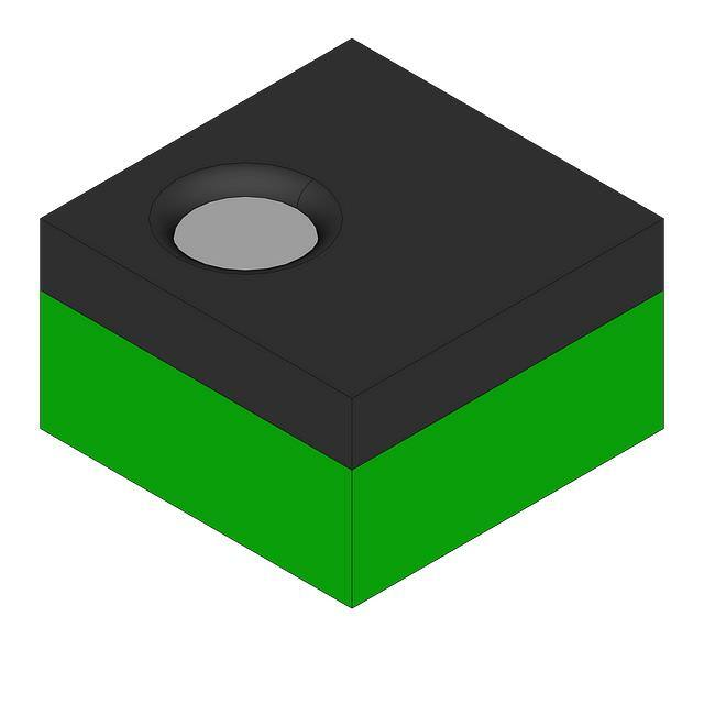
Package Dimensions
unit : mm (typ)
3433
SIDE VIEW
BOTTOM VIEW
0.195
TOP VIEW
A
2
0.5 MAX
0.2
0.33
0.08
SIDE VIEW
1
0.4
0.4
0.79
B
1.06
SANYO : WLP4J(0.79X1.06)
Pin Assignment
Top view
Ball side view
B
VDD
SCL
SCL
VDD
B
A
SDA
GND
GND
SDA
A
1
2
2
1
0.79 x 1.06 tmax:0.50mm
Pin Descriptions
PIN.A1
SDA
Serial data input/output
PIN.A2
GND
Ground
PIN.B1
VDD
Power supply
PIN.B2
SCL
Serial clock input
Block Diagram
SDA
X decoder
Serial controller
Condition detector
Address generator
I/O Buffer
SCL
Input Buffer
Write controller
High voltage generator
EEPROM Array
Y decoder & Sense AMP
Serial-Parallel converter
No.A2068-2/11
�LE24L042CS-B
Specifications
Absolute Maximum Ratings
Parameter
Supply voltage
Symbol
Conditions
Ratings
VCC
DC input voltage
Over-shoot voltage
Storage temperature
Below 20ns
Unit
-0.5 to +4.6
V
-0.5 to VDD+0.5
V
-1.0 to VDD+1.0
V
-65 to +150
°C
Tstg
Note: If an electrical stress exceeding the maximum rating is applied, the device may be damaged.
Stresses exceeding Maximum Ratings may damage the device. Maximum Ratings are stress ratings only. Functional operation above the Recommended Operating
Conditions is not implied. Extended exposure to stresses above the Recommended Operating Conditions may affect device reliability.
Operating Conditions
Parameter
Symbol
Conditions
Ratings
Operating supply voltage
Operating temperature
Unit
1.7 to 3.6
V
-40 to +85
°C
DC Electrical Characteristics
Parameter
Symbol
VDD=1.7V to 3.6V
Conditions
min
typ
Unit
max
Supply current at reading
ICC1
f=400kHz
Supply current at writing
ICC2
Standby current
ISB
Input leakage current
ILI
VIN=GND to VDD
-2.0
+2.0
μA
Output leakage current (SDA)
ILO
VOUT=GND to VDD
-2.0
+2.0
μA
Input low voltage
VIL
VDD*0.2
V
Input low voltage (CMOS)
VILC
Input high voltage
VIH
Input high voltage (CMOS)
VIHC
Output low voltage
VOL
0.5
mA
f=400kHz, tWC=10ms
3
mA
VIN=VDD or GND
2
μA
0.2
V
VDD*0.8
V
VDD-0.2
V
IOL=0.7mA,VDD=1.7V
0.2
V
IOL=1.0mA,VDD=2.5V
0.4
V
Capacitance/Ta=25°C, f=1MHz
Parameter
Symbol
Conditions
max
Unit
In/Output pin capacitance
CI/O
VI/O=0V (SDA)
10
pF
Input pin capacitance
CI
VIN=0V (other than SDA)
10
pF
Note: This parameter is sampled and not 100% tested.
VDD
AC Electric Characteristics
Input pulse level
0.1×VDD to 0.9×VDD
Input pulse rise / fall time
20ns
Output detection voltage
0.5×VDD
Output load
50pF+Pull up resistor 3.0kΩ
R=3.0kΩ
SDA
C=50pF
Output Load Circuit
No.A2068-3/11
�LE24L042CS-B
Parameter
VDD=1.7V to 3.6V
Symbol
min
unit
typ
max
Slave mode SCL clock frequency
fSCLS
SCL clock low time
tLOW
1200
0
400
kHz
ns
SCL clock high time
tHIGH
600
ns
SDA output delay time
tAA
100
SDA data output hold time
tDH
100
ns
Start condition setup time
tSU.STA
600
ns
Start condition hold time
tHD.STA
600
ns
Data in setup time
tSU.DAT
100
ns
Data in hold time
tHD.DAT
0
ns
Stop condition setup time
tSU.STO
600
SCL SDA rise time
tR
300
ns
SCL SDA fall time
tF
300
ns
900
ns
ns
Bus release time
tBUF
Noise suppression time
tSP
1200
100
ns
ns
Write cycle time
tWC
10
ms
Bus Timing
tF
tHIGH
tLOW
tR
SCL
tSP
tSU.STA
tHD.STA
tHD.DAT
tHD.STA
tSU.STO
SDA/IN
tSP
tBUF
tDH
tAA
SDA/OUT
Write Timing
tWC
SCL
SDA
D0
Write data
Acknowledge
Stop
condition
Start
condition
Pin Functions
SCL (serial clock input) pin
The SCL pin is a serial clock input pin that processes signals at the rising and falling edges of SCL clock signals.
This pin must be pulled up by a resistor to the VDD level and wired-ORed with an open drain (or open collector)
output device for use.
SDA (serial data input/output) pin
The SDA pin is used to transfer serial data to the input/output, and it consists of a signal input pin and n-channel
transistor open drain output pin.
Like the SCL pin, the SDA pin must be pulled up by a resistor to the VDD level and wired-ORed with an open drain
(or open collector) output device for use.
No.A2068-4/11
�LE24L042CS-B
Functional Description
1 Start condition
When the SCL line is at the high level, the start condition is established by changing the SDA line from high to low.
The operation of the EEPROM as a slave starts in the start condition.
2 Stop condition
When the SCL line is at the high level, the stop condition is established by changing the SDA line from low to high.
When the device is set up for the read sequence, the read operation is suspended when the stop condition is received,
and the device is set to standby mode. When it is set up for the write sequence, the capture of the write data is ended
when the stop condition is received, and the EEPROM internal write operation is started.
tSU.STA
tHD.STA
tSU.STO
SCL
SDA
Stop
condition
Start
condition
3 Data transfer
Data is transferred by changing the SDA line while the SCL line is low. When the SDA line is changed while the SCL
line is high, the resulting condition will be recognized as the start or stop condition.
tSU.DAT
tHD.DAT
SCL
SDA
4 Acknowledge
During data transfer, 8 bits are transferred in succession, and then in the ninth clock cycle period the device on the
system bus receiving the data sets the SDA line to low, and sends the acknowledge signal indicating that the data has
been received. The acknowledge signal is not sent during an EEPROM internal write operation.
SCL
(EEPROM input)
1
8
9
SDA
(Master output)
SDA
(EEPROM output)
Start
condition
Acknowledge
bit output
tAA
tDH
No.A2068-5/11
�LE24L042CS-B
5 Device addressing
For the purposes of communication, the master device in the system generates the start condition for the slave device.
Communication with a particular slave device is enabled by sending along the SDA bus the device address, which is 7
bits long, and the read/write command code, which is 1 bit long, immediately following the start condition.
The upper four bits of the device address are called the device code which, for this product, is fixed as “1010.” This
device has the upper 2-bit of the Slave Device address as the Slave address (S1, S2), which fixed internally. The value
of Slave address are S1=0, S2=0.
When the device code input from SDA and the slave addresses are compared with the product’s device code and slave
addresses that were set at the mounting stage and found to match, the product sends the acknowledge signal during
the ninth clock cycle period, and initiates the read or write operation in accordance with the read or write command
code. If they do not match, the EEPROM returns to standby mode. When a read operation is performed immediately
after the slave device has been switched, the random read command must be used.
Slave
Address
Device code
LE24L042
1
MSB
0
1
0
S2
Device Address word
S1
Memory
Address
A8
R/W
LSB
No.A2068-6/11
�LE24L042CS-B
6 EEPROM write operation
6-1. Byte writing
When the EEPROM receives the 7-bit device address and write command code “0” after the start condition, it
generates an acknowledge signal. After this, if it receives the 8-bit word address, generates an acknowledge signal,
receives the 8-bit write data, generates an acknowledge signal and then receives the stop condition, the internal write
operation of the EEPROM in the designated memory address will start. Rewriting is completed in the tWC period
after the stop condition. During an EEPROM internal write operation, no input is accepted and no acknowledge
signals are generated.
SDA
1
0
1
0 S2 S1 A8 W
Data
A7 A6 A5 A4 A3 A2 A1 A0
Stop
Start
Word_Address
D7 D6 D5 D4 D3 D2 D1 D0
ACK
ACK
R/W
ACK
6-2. Page writing
This product enables pages with up to 16 bytes to be written. The basic data transfer procedure is the same as for byte
writing: Following the start condition, the 7-bit device address and write command code “0,” word address (n), and
data (n) are input in this order while confirming acknowledge “0” every 9 bits. The page write mode is established if,
after data (n) is input, the write data (n+1) is input without inputting the stop condition. After this, the write data
equivalent to the largest page size can be received by a continuous process of repeating the receiving of the 8-bit
write data and generating the acknowledge signals.
At the point when the write data (n+1) has been input, the lower 4 bits (A0-A3) of the word addresses are
automatically incremented to form the (n+1) address. In this way, the write data can be successively input, and the
word address on the page is incremented each time the write data is input. If the write data exceeds 16 bytes or the
last address of the page is exceeded, the word address on the page is rolled over. Write data will be input into the
same address two or more times, but in such cases the write data that was input last will take effect. Finally, the
EEPROM internal write operation corresponding to the page size for which the write data is received starts from the
designated memory address when the stop condition is received.
SDA
Start
Memory_Address(n)
1
1
0
0 S2 S1 A8 W
A7 A6 A5 A4 A3 A2 A1 A0
Data(n)
Data(n+1)
D7 D6 D5 D4 D3 D2 D1 D0
D7 D6 ... D1 D0
ACK
ACK
R/W
ACK
ACK
D7 D6 ... D1 D0
D7 D6 ... D1 D0
D7 D6 ... D1 D0
ACK
D7 D6 ... D1 D0
ACK
Stop
Data(n+x)
ACK
6-3. Acknowledge polling
Acknowledge polling is used to find out when the EEPROM internal write operation is completed. When the stop
condition is received and the EEPROM starts rewriting, all operations are prohibited, and no response can be given to
the signals sent by the master device. Therefore, in order to find out when the EEPROM internal write operation is
completed, the start condition, device address and write command code are sent from the master device to the
EEPROM (slave device), and the response of the slave device is detected.
In other words, if the slave device does not send the acknowledge signal, it means that the internal write operation is
in progress; conversely, if it does send the acknowledge signal, it means that the internal write operation has been
completed.
0
1
0 S2 S1 A8 W
During Write
1
NO ACK
R/W
0
1
No Write
Start
1
Start
SDA
Start
During Write
0 S2 S1 A8 W
NO ACK
R/W
1
0
1
0 S2 S1 A8 W
ACK
R/W
No.A2068-7/11
�LE24L042CS-B
7 EEPROM read operations
7-1. Current address reading
The address equivalent to the memory address accessed last +1 is held as the internal address of the EEPROM for
both write* and read operations. Therefore, provided that the master device has recognized the position of the
EEPROM address pointer, data can be read from the memory address with the current address pointer without
specifying the word address.
As with writing, current address reading involves receiving the 7-bit device address and read command code “1”
following the start condition, at which time the EEPROM generates an acknowledge signal. After this, the 8-bit data
of the (n+1) address is output serially starting with the highest bits. After the 8 bits have been output, by not sending
an acknowledge signal and inputting the stop condition, the EEPROM completes the read operation and is set to
standby mode.
If the previous read address is the last address, the address for the current address reading is rolled over to become
address 0.
*: If the write data is 1 or more bytes but less than 16 bytes, the current address after page writing is the address
equivalent to the number of bytes to be written in the specified word address +1. If the write data is 16 or more bytes,
it is the designated word address. If the last address (A3-A0=1111b) on the page has been designated by byte write as
the word address, the first address (A3-A0=0000b) on the page serves as the internal address after writing.
1
0
1
0 S2 S1 A8 R
Data(n+1)
Stop
SDA
Start
Device_Address
D7 D6 D5 D4 D3 D2 D1 D0
ACK
R/W
NO ACK
7-2. Random read
Random read is a mode in which any memory address is specified and its data read. The address is specified by a
dummy write input.
First, when the EEPROM receives the 7-bit device address and write command code “0” following the start condition,
it generates an acknowledge signal. It then receives the 8-bit word address, and generates an acknowledge signal.
Through these operations, the word address is loaded into the address counter inside the EEPROM.
Next, the start condition is input again and the current read is initiated. This causes the data of the word address that
was input using the dummy write input to be output. If, after the data is output, an acknowledge signal is not sent and
the stop condition is input, reading is completed, and the EEPROM returns to standby mode.
0
1
0 S2 S1 A8 W
Device_Address
D7 D6 D5 D4 D3 D2 D1 D0
1
0
1
0 S2 S1 A8 R
ACK
ACK
R/W
Data(n)
D7 D6 ... D1 D0
ACK
R/W
Stop
1
Memory_Address
Start
SDA
Start
Device_Address
NO ACK
Current Read
Dummy Write
SDA
Start
Device_Address
1
0
1
0 S2 S1 A8 R
Data(n)
Data(n+1)
Data(n+2)
Data(n+x)
D7 D6 ... D1 D0
D7 D6 ... D1 D0
D7 D6 ... D1 D0
D7 D6 ... D1 D0
ACK
R/W
ACK
ACK
ACK
Stop
7-3. Sequential read
In this mode, the data is read continuously, and sequential read operations can be performed with both current address
read and random read. If, after the 8-bit data has been output, acknowledge “0” is input and reading is continued
without issuing the stop condition, the address is incremented, and the data of the next address is output.
If acknowledge “0” continues to be input after the data has been output in this way, the data is successively output
while the address is incremented. When the last address is reached, it is rolled over to address 0, and the data
continues to be read. As with current address read and random read, the operation is completed by inputting the stop
condition without sending an acknowledge signal.
NO ACK
No.A2068-8/11
�LE24L042CS-B
Application Notes
1) Software reset function
Software reset (start condition + 9 dummy clock cycles + start condition), shown in the figure below, is executed in
order to avoid erroneous operation after power-on and to reset while the command input sequence. During the
dummy clock input period, the SDA bus must be opened (set to high by a pull-up resistor). Since it is possible for
the ACK output and read data to be output from the EEPROM during the dummy clock period, forcibly entering H
will result in an overcurrent flow.
Note that this software reset function does not work during the internal write cycle.
Dummy clock × 9
SCL
1
2
8
9
SDA
Start
condition
Start
condition
2) Pull-up resistor of SDA pin
Due to the demands of the I2C bus protocol function, the SDA pin must be connected to a pull-up resistor (with a
resistance from several kΩ to several tens of kΩ) without fail. The appropriate value must be selected for this
resistance (RPU) on the basis of the VIL and IIL of the microcontroller and other devices controlling this product as
well as the VOL–IOL characteristics of the product. Generally, when the resistance is too high, the operating
frequency will be restricted; conversely, when it is too low, the operating current consumption will increase.
RPU maximum resistance
The maximum resistance must be set in such a way that the bus potential, which is determined by the sum total (IL)
of the input leaks of the devices connected to the SDA bus and by RPU, can completely satisfy the input high level
(VIH min) of the microcontroller and EEPROM. However, a resistance value that satisfies SDA rise time tR and fall
time tF must be set.
RPU maximum value = (VDD - VIH)/IL
Example: When VDD=2.5V and IL= 2μA
RPU maximum value = (2.5V − 2.5V × 0.8)/2μA = 250kΩ
RPU minimum value
A resistance corresponding to the low-level output
voltage (VOL max) of EEPROM must be set.
RPU minimum value = (VDD − VOL)/IOL
RPU
SDA
Master
Device
IL
EEPROM
CBUS
IL
Example: When VDD=2.5V, VOL = 0.4V and IOL = 1mA
RPU minimum value = (2.5V − 0.4)/1mA = 2.1kΩ
Recommended RPU setting
RPU is set to strike a good balance between the operating frequency requirements and power consumption. If it is
assumed that the SDA load capacitance is 50pF and the SDA output data strobe time is 500ns, RPU will be about
RPU = 500ns/50pF = 10kΩ.
No.A2068-9/11
�LE24L042CS-B
3) Precautions when turning on the power
This product contains a power-on reset circuit for preventing the inadvertent writing of data when the power is
turned on. The following conditions must be met in order to ensure stable operation of this circuit. No data
guarantees are given in the event of an instantaneous power failure during the internal write operation.
Item
VDD=1.7 to 3.6V
Symbol
min
Power rise time
tRISE
Power off time
tOFF
Power bottom voltage
Vbot
typ
unit
max
100
10
ms
ms
0.2
V
tRISE
VDD
tOFF
Vbot
0V
Notes:
1) The SDA pin must be set to high and the SCL pin to low or high.
2) Steps must be taken to ensure that the SDA and SCL pins are not placed in a high-impedance state.
A. If it is not possible to satisfy the instruction 1 in Note above, and SDA is set to low during power rise
After the power has stabilized, the SCL and SDA pins must be controlled as shown below, with both pins set to high.
VDD
VDD
tLOW
SCL
SCL
SDA
SDA
tDH
tSU.DAT
tSU.DAT
B. If it is not possible to satisfy the instruction 2 in Note above
After the power has stabilized, software reset must be executed.
C. If it is not possible to satisfy the instructions both 1 and 2 in Note above
After the power has stabilized, the steps in A must be executed, then software reset must be executed.
4) Noise filter for the SCL and SDA pins
This product contains a filter circuit for eliminating noise at the SCL and SDA pins. Pulses of 100ns or less are not
recognized because of this function.
5) Function to inhibit writing when supply voltage is low
This product contains a supply voltage monitoring circuit that inhibits inadvertent writing below the guaranteed
operating supply voltage range. The data is protected by ensuring that write operations are not started at voltages
(typ.) of 1.3V and below.
No.A2068-10/11
�LE24L042CS-B
6) Slave address settings
This product does not come with any slave address pins, but the information of the S0, S1 and S2 slave addresses is
held internally. S1 = 0 and S2 = 0 were set for the slave addresses before shipment. During device addressing, these
slave address codes must be executed following the device code.
ON Semiconductor and the ON logo are registered trademarks of Semiconductor Components Industries, LLC (SCILLC). SCILLC owns the rights to a number
of patents, trademarks, copyrights, trade secrets, and other intellectual property. A listing of SCILLC’s product/patent coverage may be accessed at
www.onsemi.com/site/pdf/Patent-Marking.pdf. SCILLC reserves the right to make changes without further notice to any products herein. SCILLC makes no
warranty, representation or guarantee regarding the suitability of its products for any particular purpose, nor does SCILLC assume any liability arising out of the
application or use of any product or circuit, and specifically disclaims any and all liability, including without limitation special, consequential or incidental
damages. “Typical” parameters which may be provided in SCILLC data sheets and/or specifications can and do vary in different applications and actual
performance may vary over time. All operating parameters, including “Typicals” must be validated for each customer application by customer’s technical
experts. SCILLC does not convey any license under its patent rights nor the rights of others. SCILLC products are not designed, intended, or authorized for use
as components in systems intended for surgical implant into the body, or other applications intended to support or sustain life, or for any other application in
which the failure of the SCILLC product could create a situation where personal injury or death may occur. Should Buyer purchase or use SCILLC products for
any such unintended or unauthorized application, Buyer shall indemnify and hold SCILLC and its officers, employees, subsidiaries, affiliates, and distributors
harmless against all claims, costs, damages, and expenses, and reasonable attorney fees arising out of, directly or indirectly, any claim of personal injury or
death associated with such unintended or unauthorized use, even if such claim alleges that SCILLC was negligent regarding the design or manufacture of the
part. SCILLC is an Equal Opportunity/Affirmative Action Employer. This literature is subject to all applicable copyright laws and is not for resale in any manner.
PS No.A2068-11/11
�Mouser Electronics
Authorized Distributor
Click to View Pricing, Inventory, Delivery & Lifecycle Information:
ON Semiconductor:
LE24L042CS-B-SH LE24L042CS-B-TFM-H
�


 工商网监
湘ICP备2023018690号
工商网监
湘ICP备2023018690号
