Is Now Part of
To learn more about ON Semiconductor, please visit our website at
www.onsemi.com
Please note: As part of the Fairchild Semiconductor integration, some of the Fairchild orderable part numbers
will need to change in order to meet ON Semiconductor’s system requirements. Since the ON Semiconductor
product management systems do not have the ability to manage part nomenclature that utilizes an underscore
(_), the underscore (_) in the Fairchild part numbers will be changed to a dash (-). This document may contain
device numbers with an underscore (_). Please check the ON Semiconductor website to verify the updated
device numbers. The most current and up-to-date ordering information can be found at www.onsemi.com. Please
email any questions regarding the system integration to Fairchild_questions@onsemi.com.
ON Semiconductor and the ON Semiconductor logo are trademarks of Semiconductor Components Industries, LLC dba ON Semiconductor or its subsidiaries in the United States and/or other countries. ON Semiconductor owns the rights to a number
of patents, trademarks, copyrights, trade secrets, and other intellectual property. A listing of ON Semiconductor’s product/patent coverage may be accessed at www.onsemi.com/site/pdf/Patent-Marking.pdf. ON Semiconductor reserves the right
to make changes without further notice to any products herein. ON Semiconductor makes no warranty, representation or guarantee regarding the suitability of its products for any particular purpose, nor does ON Semiconductor assume any liability
arising out of the application or use of any product or circuit, and specifically disclaims any and all liability, including without limitation special, consequential or incidental damages. Buyer is responsible for its products and applications using ON
Semiconductor products, including compliance with all laws, regulations and safety requirements or standards, regardless of any support or applications information provided by ON Semiconductor. “Typical” parameters which may be provided in ON
Semiconductor data sheets and/or specifications can and do vary in different applications and actual performance may vary over time. All operating parameters, including “Typicals” must be validated for each customer application by customer’s
technical experts. ON Semiconductor does not convey any license under its patent rights nor the rights of others. ON Semiconductor products are not designed, intended, or authorized for use as a critical component in life support systems or any FDA
Class 3 medical devices or medical devices with a same or similar classification in a foreign jurisdiction or any devices intended for implantation in the human body. Should Buyer purchase or use ON Semiconductor products for any such unintended
or unauthorized application, Buyer shall indemnify and hold ON Semiconductor and its officers, employees, subsidiaries, affiliates, and distributors harmless against all claims, costs, damages, and expenses, and reasonable attorney fees arising out
of, directly or indirectly, any claim of personal injury or death associated with such unintended or unauthorized use, even if such claim alleges that ON Semiconductor was negligent regarding the design or manufacture of the part. ON Semiconductor
is an Equal Opportunity/Affirmative Action Employer. This literature is subject to all applicable copyright laws and is not for resale in any manner.
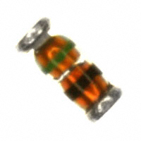
�LL4148
Small Signal Diode
Cathode Band
COLOR BAND MARKING
1ST BAND
Black
SOD80
The 1st Band indicates the cathode band
Ordering Information
Part Number
Device Marking
Package
Packing Method
LL4148
Color Band Marking
SOD-80 2L
Tape and Reel, 7 inch Reel, 2500 pcs
Absolute Maximum Ratings(1), (2)
Stresses exceeding the absolute maximum ratings may damage the device. The device may not function or be operable above the recommended operating conditions and stressing the parts to these levels is not recommended. In addition, extended exposure to stresses above the recommended operating conditions may affect device reliability. The
absolute maximum ratings are stress ratings only. Values are at TA = 25°C unless otherwise noted.
Symbol
Parameter
Value
Unit
VRRM
Maximum Repetitive Reverse Voltage
100
V
IF(AV)
Average Rectified Forward Current
200
mA
Recurrent Peak Forward Current
500
mA
If
Pulse Width = 1.0 s
1.0
Pulse Width = 1.0 μs
2.0
IFSM
Non-Repetitive Peak
Forward Surge Current
TSTG
Storage Temperature Range
-65 to +200
°C
Operating Junction Temperature Range
-55 to +175
°C
TJ
A
Notes:
1. These ratings are based on a maximum junction temperature of 200°C.
2. These are steady-state limits. Fairchild Semiconductor should be consulted on applications involving pulsed or
low-duty-cycle operations.
© 2005 Fairchild Semiconductor Corporation
LL4148 Rev. 1.8
www.fairchildsemi.com
LL4148 — Small Signal Diode
January 2016
�Values are at TA = 25°C unless otherwise noted.
Symbol
PD
RθJA
Parameter
Value
Unit
Power Dissipation
500
mW
Thermal Resistance, Junction-to-Ambient
300
°C/W
Note:
3. JEDEC Standard 51-3 method (PCB Board size 76 x 114 x 0.6Tmm3)
Electrical Characteristics
Values are at TA = 25°C unless otherwise noted.
Symbol
Parameter
VR
Breakdown Voltage
VF
Forward Voltage
IR
Reverse Leakage
CT
trr
Conditions
Min.
IR = 100 μA
100
IR = 5.0 μA
75
Max.
Unit
V
IF = 10 mA
1.0
V
VR = 20 V
25
nA
VR = 20 V, TA = 150°C
50
μA
Total Capacitance
VR = 0, f = 1.0 MHz
4.0
pF
Reverse Recovery Time
IF = 10 mA, VR = 6.0 V (60 mA),
Irr = 1.0 mA, RL = 100 Ω
4.0
ns
© 2005 Fairchild Semiconductor Corporation
LL4148 Rev. 1.8
www.fairchildsemi.com
2
LL4148 — Small Signal Diode
Thermal Characteristics(3)
�LL4148 — Small Signal Diode
Typical Performance Characteristics
160
120
o
Ta=25 C
o
Ta= 25 C
100
Reverse Current, I R
R
Reverse Voltage, V R R [V]
[nA]
150
140
130
120
80
60
40
20
0
110
1
2
3
5
10
20
30
50
100
10
20
50
70
100
Reverse Voltage, VR [V]
Reverse Current, IR [uA]
Figure 2. Reverse Current vs. Reverse Voltage
IR - 10 to 100 V
Figure 1. Reverse Voltage vs. Reverse Current
BV - 1.0 to 100 μA
750
550
o
o
Ta= 25 C
Ta= 25 C
700
Forward Voltage, V
VF R [mV]
Forward Voltage, VF F [mV]
500
650
450
600
400
550
350
500
300
250
30
Reverse Voltage, VR [V]
450
1
2
3
5
10
20
30
50
0.1
100
0.2
Forward Current, IF [uA]
0.3
0.5
1
2
3
5
10
Forward Current, IF [mA]
Figure 4. Forward Voltage vs. Forward Current
VF - 0.1 to 10 mA
Figure 3. Forward Voltage vs. Forward Current
VF - 1 to 100 μA
1.6
900
o
Ta= 25 C
Typical
[
Forward Voltage, VFF [mV]
Forward Voltage, VF F [mV]
800
1.4
o
Ta= -40 C
700
1.2
o
Ta= 25 C
600
1.0
500
o
Ta= +65 C
400
0.8
300
0.6
10
20
30
50
100
200
300
500
800
0.01
Forward Current, IF [mA]
0.1
0.3
1
3
10
Forward Current, IF [mA]
Figure 6. Forward Voltage vs. Ambient Temperature
VF - 0.01 - 20 mA (-40 to +65 °C)
Figure 5. Forward Voltage vs. Forward Current
VF - 10 to 800 mA
© 2005 Fairchild Semiconductor Corporation
LL4148 Rev. 1.8
0.03
www.fairchildsemi.com
3
�LL4148 — Small Signal Diode
Typical Performance Characteristics (Continued)
4.0
0.90
[ns]
o
o
Ta== 25
25°C
Ta
C
3.5
Reverse Recovery Time, trr
Total Capacitance (pF)
rr
TA = 25 C
0.85
0.80
2
4
6
8
10
12
2.5
2.0
1.5
1.0
10
0.75
0
3.0
14
30
40
50
60
Figure 8. Reverse Recovery Time vs.
Reverse Recovery Current
Figure 7. Total Capacitance
500
Power Dissipation, PD [mW]
500
400
Current (mA)
20
Reverse Recovery Current, Irr [mA]
REVERSE VOLTAGE (V)
400
300
DO-35
SOD80
300
IF(A V) AV
ERAG
E RE
CTIF
IED C
URRE
NT mA
200
100
200
100
0
0
50
100
0
150
0
o
100
150
200
Temperature [ C]
Figure 10. Power Derating Curve
Figure 9. Average Rectified Current (IF(AV))
vs. Ambient Temperature (TA)
© 2005 Fairchild Semiconductor Corporation
LL4148 Rev. 1.8
50
o
Ambient Temperature ( C)
www.fairchildsemi.com
4
�0.50
0.30
1.50
1.30
2.64 REF
1.40
1.20
C
0.30
R
0.20
3.60
3.30
3.30
0.50
1.65
1.10
0.50
LAND PATTERN RECOMMENDATION
NOTES: UNLESS OTHERWISE SPECIFIED
A) PACKAGE STANDARD REFERENCE:
JEDEC DO-213, VARIATION AC.
B) ALL DIMENSIONS ARE IN MILLIMETERS.
C
CORNER RADIUS IS OPTIONAL.
D) LAND PATTERN RECOMMENDATION PER IPC DIOMELF3414N
E) DRAWING FILE NAME: SOD80A
REV3
�ON Semiconductor and
are trademarks of Semiconductor Components Industries, LLC dba ON Semiconductor or its subsidiaries in the United States and/or other countries.
ON Semiconductor owns the rights to a number of patents, trademarks, copyrights, trade secrets, and other intellectual property. A listing of ON Semiconductor’s product/patent
coverage may be accessed at www.onsemi.com/site/pdf/Patent−Marking.pdf. ON Semiconductor reserves the right to make changes without further notice to any products herein.
ON Semiconductor makes no warranty, representation or guarantee regarding the suitability of its products for any particular purpose, nor does ON Semiconductor assume any liability
arising out of the application or use of any product or circuit, and specifically disclaims any and all liability, including without limitation special, consequential or incidental damages.
Buyer is responsible for its products and applications using ON Semiconductor products, including compliance with all laws, regulations and safety requirements or standards,
regardless of any support or applications information provided by ON Semiconductor. “Typical” parameters which may be provided in ON Semiconductor data sheets and/or
specifications can and do vary in different applications and actual performance may vary over time. All operating parameters, including “Typicals” must be validated for each customer
application by customer’s technical experts. ON Semiconductor does not convey any license under its patent rights nor the rights of others. ON Semiconductor products are not
designed, intended, or authorized for use as a critical component in life support systems or any FDA Class 3 medical devices or medical devices with a same or similar classification
in a foreign jurisdiction or any devices intended for implantation in the human body. Should Buyer purchase or use ON Semiconductor products for any such unintended or unauthorized
application, Buyer shall indemnify and hold ON Semiconductor and its officers, employees, subsidiaries, affiliates, and distributors harmless against all claims, costs, damages, and
expenses, and reasonable attorney fees arising out of, directly or indirectly, any claim of personal injury or death associated with such unintended or unauthorized use, even if such
claim alleges that ON Semiconductor was negligent regarding the design or manufacture of the part. ON Semiconductor is an Equal Opportunity/Affirmative Action Employer. This
literature is subject to all applicable copyright laws and is not for resale in any manner.
PUBLICATION ORDERING INFORMATION
LITERATURE FULFILLMENT:
Literature Distribution Center for ON Semiconductor
19521 E. 32nd Pkwy, Aurora, Colorado 80011 USA
Phone: 303−675−2175 or 800−344−3860 Toll Free USA/Canada
Fax: 303−675−2176 or 800−344−3867 Toll Free USA/Canada
Email: orderlit@onsemi.com
© Semiconductor Components Industries, LLC
N. American Technical Support: 800−282−9855 Toll Free
USA/Canada
Europe, Middle East and Africa Technical Support:
Phone: 421 33 790 2910
Japan Customer Focus Center
Phone: 81−3−5817−1050
www.onsemi.com
1
ON Semiconductor Website: www.onsemi.com
Order Literature: http://www.onsemi.com/orderlit
For additional information, please contact your local
Sales Representative
www.onsemi.com
�