Is Now Part of
To learn more about ON Semiconductor, please visit our website at
www.onsemi.com
Please note: As part of the Fairchild Semiconductor integration, some of the Fairchild orderable part numbers
will need to change in order to meet ON Semiconductor’s system requirements. Since the ON Semiconductor
product management systems do not have the ability to manage part nomenclature that utilizes an underscore
(_), the underscore (_) in the Fairchild part numbers will be changed to a dash (-). This document may contain
device numbers with an underscore (_). Please check the ON Semiconductor website to verify the updated
device numbers. The most current and up-to-date ordering information can be found at www.onsemi.com. Please
email any questions regarding the system integration to Fairchild_questions@onsemi.com.
ON Semiconductor and the ON Semiconductor logo are trademarks of Semiconductor Components Industries, LLC dba ON Semiconductor or its subsidiaries in the United States and/or other countries. ON Semiconductor owns the rights to a number
of patents, trademarks, copyrights, trade secrets, and other intellectual property. A listing of ON Semiconductor’s product/patent coverage may be accessed at www.onsemi.com/site/pdf/Patent-Marking.pdf. ON Semiconductor reserves the right
to make changes without further notice to any products herein. ON Semiconductor makes no warranty, representation or guarantee regarding the suitability of its products for any particular purpose, nor does ON Semiconductor assume any liability
arising out of the application or use of any product or circuit, and specifically disclaims any and all liability, including without limitation special, consequential or incidental damages. Buyer is responsible for its products and applications using ON
Semiconductor products, including compliance with all laws, regulations and safety requirements or standards, regardless of any support or applications information provided by ON Semiconductor. “Typical” parameters which may be provided in ON
Semiconductor data sheets and/or specifications can and do vary in different applications and actual performance may vary over time. All operating parameters, including “Typicals” must be validated for each customer application by customer’s
technical experts. ON Semiconductor does not convey any license under its patent rights nor the rights of others. ON Semiconductor products are not designed, intended, or authorized for use as a critical component in life support systems or any FDA
Class 3 medical devices or medical devices with a same or similar classification in a foreign jurisdiction or any devices intended for implantation in the human body. Should Buyer purchase or use ON Semiconductor products for any such unintended
or unauthorized application, Buyer shall indemnify and hold ON Semiconductor and its officers, employees, subsidiaries, affiliates, and distributors harmless against all claims, costs, damages, and expenses, and reasonable attorney fees arising out
of, directly or indirectly, any claim of personal injury or death associated with such unintended or unauthorized use, even if such claim alleges that ON Semiconductor was negligent regarding the design or manufacture of the part. ON Semiconductor
is an Equal Opportunity/Affirmative Action Employer. This literature is subject to all applicable copyright laws and is not for resale in any manner.
�LM317M
3-Terminal 0.5A Positive Adjustable Regulator
Features
Description
•
•
•
•
•
•
The LM317M is a 3-terminal adjustable positive voltage
regulator capable of supplying in excess of 500 mA over
an output voltage range of 1.2 V to 37 V. This voltage regulator is exceptionally easy to use and requires only two
external resistors to set the output voltage.
Output Current in Excess of 0.5 A
Output Adjustable Between 1.2 V and 37 V
Internal Thermal Overload Protection
Internal Short-Circuit Current Limiting
Output Transistor Safe Area Compensation
Floating Operation for High Voltage Applications
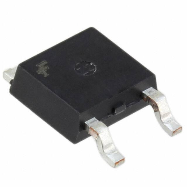
D-PAK
2
1 3
1. Adj 2. Output 3. Input
TO-220 (Single Gauge)
12 3
Ordering Information
Product Number
Marking
Package
Packing Method Operating Temperature
LM317MDTX
LM317MDT
TO-252 3L (D-PAK)
Tape and Reel
LM317MDTXM
LM317MDT
TO-252 3L (D-PAK)
Tape and Reel
LM317MT
LM317M
TO-220 3L (Single Gauge)
Rail
0 to +125°C
* Refer to below unit orientation figure for TM / TF suffix packing.
© 2003 Fairchild Semiconductor Corporation
LM317M Rev. 1.1.0
www.fairchildsemi.com
LM317M — 3-Terminal 0.5A Positive Adjustable Regulator
September 2014
�LM317M — 3-Terminal 0.5A Positive Adjustable Regulator
Block Diagram
Input
V in 3
+
-
P rote ction
Circ uitry
V olta ge
Re fe re nce
R lim it
2
Vo
Output
1
V ad j
Figure 1. Block Diagram
Absolute Maximum Ratings
Stresses exceeding the absolute maximum ratings may damage the device. The device may not function or be operable above the recommended operating conditions and stressing the parts to these levels is not recommended. In addition, extended exposure to stresses above the recommended operating conditions may affect device reliability. The
absolute maximum ratings are stress ratings only. Values are at TA = 25°C unless otherwise noted.
Symbol
VI - VO
TJ
TSTG
Parameter
Input-Output Voltage Differential
Operating Junction Temperature Range
Storage Temperature Range
Value
Unit
40
V
0 to +125
°C
-65 to +125
°C
Thermal Characteristics
Values are at TA = 25°C unless otherwise noted.
Value
Symbol
PD
Parameter
LM317MT
Power Dissipation
LM317MDTX /
LM317MDTXM(1),(2)
Internally Limited
Unit
W
RθJC
Thermal Resistance, Junction to Case
5
-
°C/W
RθJA
Thermal Resistance, Junction to Ambient
81
100
°C/W
Notes:
1. Thermal resistance test board - size: 76.2 mm x 114.3 mm x 1.6 mm (1S0P),
JEDEC standard: JESD51-3, JESD51-7
2. Assume no ambient airflow
© 2003 Fairchild Semiconductor Corporation
LM317M Rev. 1.1.0
www.fairchildsemi.com
2
�VI - VO = 5 V, IO = 0.1 A, 0°C ≤ TJ ≤ +125°C, PDMAX = 7.5 W, unless otherwise specified.
Symbol
Rline
Rload
IADJ
Parameter
Line Regulation(3)
Load Regulation(3)
Conditions
Min.
Typ.
TA = +25°C, 3 V ≤ VI −VO ≤ 40 V
0.01
0.04
0.02
0.07
TA = +25°C, 10 mA ≤ IO ≤ 0.5 A,
VO ≤ 5 V
5
25
mV
TA = +25°C, 10 mA ≤ IO ≤ 0.5 A,
VO ≥ 5 V
0.1
0.5
%/VO
10 mA ≤ IO ≤ 0.5 A, VO ≤ 5 V
20
70
mV
0.3
1.5
%/VO
-
50
100
μA
0.2
5.0
μA
1.25
1.30
V
Adjustment Pin Current
3 V ≤ VI - VO ≤ 40 V,
10 mA ≤ IO ≤ 0.5 A, PD < PDMAX
VREF
Reference Voltage
3 V < VI - VO < 40 V,
10 mA ≤ IO ≤ 0.5 A, PD < PDMAX
STT
Temperature Stability
TJ = 0°C to +125°C
0.7
Minimum Load Current to
Maintain Regulation
VI - VO = 40 V
3.5
eN
RR
ST
1.20
VI - VO ≤ 15 V, PD < PDMAX
0.5
0.9
Maximum Output Current
VI - VO = 40 V
PD < PDMAX, TA = +25°C
0.15
0.25
RMS Noise, % of VOUT
TA = +25°C, 10 Hz < f < 10 kHz
Ripple Rejection
Long-Term Stability
%/ V
10 mA ≤ IO ≤ 0.5 A, VO ≥ 5V
Adjustment Pin Current Change
IO(MAX)
Unit
3 V ≤ VI −VO ≤ 40 V
ΔIADJ
IL(MIN)
Max.
VO = 10 V, f = 120 Hz,
without CADJ
%/VO
10.0
A
0.003
66
mA
%/VO
65
dB
VO = 10 V, f = 120 Hz,
CADJ = 10 μF(4)
80
TJ = +125°C, 1000 Hours
0.3
1
%/
1000Hrs
Notes:
3. Load and Line regulation are specified at constant junction temperature. Change in VO due to heating effects must
be taken into account separately. Pulse testing with low duty cycle is used.
4. CADJ, when used, is connected between the adjustment pin and ground.
© 2003 Fairchild Semiconductor Corporation
LM317M Rev. 1.1.0
www.fairchildsemi.com
3
LM317M — 3-Terminal 0.5A Positive Adjustable Regulator
Electrical Characteristics
�Figure 2. Minimum Load Current
Figure 3. Peak Output Current vs. Input-Output
Differential Voltage
Figure 4. Adjustment Pin Current vs. Temperature
Figure 5. Ripple Rejection vs. Frequency
Figure 6. Load Regulation vs. Temperature
Figure 7. Line Regulation vs. Temperature
© 2003 Fairchild Semiconductor Corporation
LM317M Rev. 1.1.0
www.fairchildsemi.com
4
LM317M — 3-Terminal 0.5A Positive Adjustable Regulator
Typical Performance Characteristics
�LM317M — 3-Terminal 0.5A Positive Adjustable Regulator
Typical Performance Characteristics (Continued)
Figure 8. Output Voltage vs. Temperature
© 2003 Fairchild Semiconductor Corporation
LM317M Rev. 1.1.0
Figure 9. Thermal Shutdown
www.fairchildsemi.com
5
�D1
1N4002
Input
VO
LM317M
Output
+
120
1.0uF
VADJ
1K
720
KSP2222
TTL CONTROL
MINIMUM VO = 1.25V
Figure 10. 15V Electronic Shutdown Regulator(5)
Note:
5. D1 protects the device during an input short circuit.
VO
LM317M
Output
Input
240
1N4001
50K
VADJ
KSP2907
R2
+
1.0uF
Figure 11. Slow Turn-On Regulator
© 2003 Fairchild Semiconductor Corporation
LM317M Rev. 1.1.0
www.fairchildsemi.com
6
LM317M — 3-Terminal 0.5A Positive Adjustable Regulator
Typical Application
�IO
Input
LM317M
R1
VO
R2
Output
VADJ
IADJ
V
REF- + I
I
= ---------------≅ 1.25V
---------------- R1
OMAX
ADJ
R1
V
REF - + I
1.25V I
= --------------------≅ --------------------OMAX R1 + R2
ADJ R1 + R2
5mA < I < 500mA
O
Figure 12. Current Regulator
© 2003 Fairchild Semiconductor Corporation
LM317M Rev. 1.1.0
www.fairchildsemi.com
7
LM317M — 3-Terminal 0.5A Positive Adjustable Regulator
Typical Application (Continued)
�LM317M — 3-Terminal 0.5A Positive Adjustable Regulator
Physical Dimensions
)
$
����
������
������0,1�
�
) �����
�����
������0,1�
����
������ )
������
����
������
�
�
&
�
������0,1�
�
������0$;�
�
������
������
����
������
����
������
������0,1�
������
/$1'�3$77(51�5(&200(1'$7,21
)
%
����
������
) ������
����
)
����
������
������0,1�
������
�
) �����
�����
6((�'(7$,/�$
���� %
)
*$*(�3/$1(
����
������
) ������
������
127(6�81/(66�27+(5:,6(�63(&,),('
$����127�&203/,$17�72�-('(&�72�����9$5,$7,21�$%
�������0$;�
%����$//�',0(16,21�$5(�,1�0,//,0(7(5
&����',0(16,216�$5(�(;&/86,9(�2)�%8556�02/'�)/$6+�
6($7,1*�3/$1(
�������$1'�7,(�%$5�(;7586,216
'����/$'�3$77(51�3(5�,3&����$�$7$1'$5'�
�������72���3���;�����1
(����'5$:,1*�),/(�1$0(�0.7�72���'��5(9��
)����'2(6�127�&203/