Is Now Part of
To learn more about ON Semiconductor, please visit our website at
www.onsemi.com
Please note: As part of the Fairchild Semiconductor integration, some of the Fairchild orderable part numbers
will need to change in order to meet ON Semiconductor’s system requirements. Since the ON Semiconductor
product management systems do not have the ability to manage part nomenclature that utilizes an underscore
(_), the underscore (_) in the Fairchild part numbers will be changed to a dash (-). This document may contain
device numbers with an underscore (_). Please check the ON Semiconductor website to verify the updated
device numbers. The most current and up-to-date ordering information can be found at www.onsemi.com. Please
email any questions regarding the system integration to Fairchild_questions@onsemi.com.
ON Semiconductor and the ON Semiconductor logo are trademarks of Semiconductor Components Industries, LLC dba ON Semiconductor or its subsidiaries in the United States and/or other countries. ON Semiconductor owns the rights to a number
of patents, trademarks, copyrights, trade secrets, and other intellectual property. A listing of ON Semiconductor’s product/patent coverage may be accessed at www.onsemi.com/site/pdf/Patent-Marking.pdf. ON Semiconductor reserves the right
to make changes without further notice to any products herein. ON Semiconductor makes no warranty, representation or guarantee regarding the suitability of its products for any particular purpose, nor does ON Semiconductor assume any liability
arising out of the application or use of any product or circuit, and specifically disclaims any and all liability, including without limitation special, consequential or incidental damages. Buyer is responsible for its products and applications using ON
Semiconductor products, including compliance with all laws, regulations and safety requirements or standards, regardless of any support or applications information provided by ON Semiconductor. “Typical” parameters which may be provided in ON
Semiconductor data sheets and/or specifications can and do vary in different applications and actual performance may vary over time. All operating parameters, including “Typicals” must be validated for each customer application by customer’s
technical experts. ON Semiconductor does not convey any license under its patent rights nor the rights of others. ON Semiconductor products are not designed, intended, or authorized for use as a critical component in life support systems or any FDA
Class 3 medical devices or medical devices with a same or similar classification in a foreign jurisdiction or any devices intended for implantation in the human body. Should Buyer purchase or use ON Semiconductor products for any such unintended
or unauthorized application, Buyer shall indemnify and hold ON Semiconductor and its officers, employees, subsidiaries, affiliates, and distributors harmless against all claims, costs, damages, and expenses, and reasonable attorney fees arising out
of, directly or indirectly, any claim of personal injury or death associated with such unintended or unauthorized use, even if such claim alleges that ON Semiconductor was negligent regarding the design or manufacture of the part. ON Semiconductor
is an Equal Opportunity/Affirmative Action Employer. This literature is subject to all applicable copyright laws and is not for resale in any manner.
�www.fairchildsemi.com
LM324/LM324A, LM2902/LM2902A
Quad Operational Amplifier
Features
Description
• Internally Frequency Compensated for Unity Gain
• Large DC Voltage Gain: 100dB
• Wide Power Supply Range:
LM324/LM324A : 3V~32V (or ±1.5 ~ 16V)
LM2902/LM2902A: 3V~26V (or ±1.5V ~ 13V)
• Input Common Mode Voltage Range Includes
Ground
• Large Output Voltage Swing: 0V to VCC -1.5V
• Power Drain Suitable for Battery Operation
The LM324/LM324A, LM2902/LM2902A consist of four
independent, high gain, internally frequency compensated operational amplifiers which were designed specifically to operate from a single power supply over a
wide voltage range. operation from split power supplies
is also possible so long as the difference between the
two supplies is 3 volts to 32 volts. Application areas
include transducer amplifier, DC gain blocks and all the
conventional OP Amp circuits which now can be easily
implemented in single power supply systems.
14-DIP
1
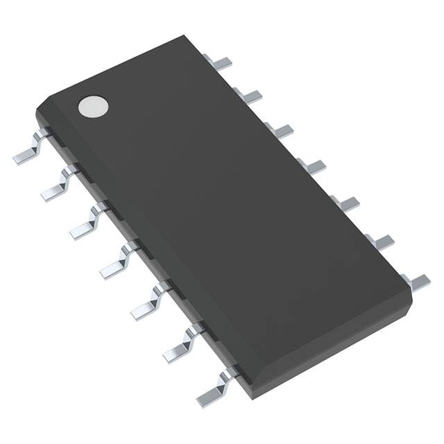
14-SOP
1
Internal Block Diagram
14 OUT4
OUT1 1
IN1 (-)
2
IN1 (+) 3
1
_ +
+
4
_
13 IN4 (-)
12 IN4 (+)
VCC 4
11 GND
IN2 (+)
5
_ +
IN2 (-)
6
2
OUT2
7
+
_
10 IN3 (+)
3
9 IN3 (-)
8 OUT3
Rev. 1.0.9
©2012 Fairchild Semiconductor Corporation
�LM324/LM324A, LM2902/LM2902A
Schematic Diagram
(One Section Only)
VCC
Q5
Q12
Q6
Q17
Q19
Q20
Q2
Q3
R1
C1
Q4
IN(-)
Q18
Q1
R2
IN(+)
Q11
OUTPUT
Q21
Q10
Q7
Q8
Q9
Q15
Q13
Q14
Q16
GND
Absolute Maximum Ratings
Parameter
Symbol
LM324/LM324A
LM2902/LM2902A
Unit
VCC
±16 or 32
±13 or 26
V
VI(DIFF)
32
26
V
Input Voltage
VI
-0.3 to +32
-0.3 to +26
V
Output Short Circuit to GND
Vcc≤15V, TA=25°C(one Amp)
-
Continuous
Continuous
-
PD
1310
640
1310
640
mW
Operating Temperature Range
TOPR
0 ~ +70
-40 ~ +85
°C
Storage Temperature Range
TSTG
-65 ~ +150
-65 ~ +150
°C
Power Supply Voltage
Differential Input Voltage
Power Dissipation, TA=25°C
14-DIP
14-SOP
Thermal Data
Parameter
Thermal Resistance Junction-Ambient Max.
14-DIP
14-SOP
2
Symbol
Value
Unit
Rθja
95
195
°C/W
�LM324/LM324A, LM2902/LM2902A
Electrical Characteristics
(VCC = 5.0V, VEE = GND, TA = 25°C, unless otherwise specified)
Parameter
Symbol
Conditions
Input Offset Voltage
VIO
Input Offset Current
LM324
LM2902
Unit
Min.
Typ.
Max.
Min.
Typ.
Max.
VCM = 0V to VCC -1.5V
VO(P) = 1.4V, RS = 0Ω
(Note1)
-
1.5
7.0
-
1.5
7.0
mV
IIO
VCM = 0V
-
3.0
50
-
3.0
50
nA
Input Bias Current
IBIAS
VCM = 0V
-
40
250
-
40
250
nA
Input Common-Mode
Voltage Range
VI(R)
Note1
0
-
VCC
-1.5
0
-
VCC
-1.5
V
Supply Current
ICC
RL = ∞,VCC = 30V
(LM2902,VCC=26V)
-
1.0
3
-
1.0
3
mA
RL = ∞,VCC = 5V
-
0.7
1.2
-
0.7
1.2
mA
VCC = 15V,RL=2kΩ
VO(P) = 1V to 11V
25
100
-
25
100
-
V/mV
RL = 2kΩ
26
-
-
22
-
-
V
RL=10kΩ
27
28
-
23
24
-
V
-
5
20
-
5
100
mV
Large Signal
Voltage Gain
Output Voltage Swing
GV
VO(H)
Note1
VO(L)
VCC = 5V, RL=10kΩ
Common-Mode
Rejection Ratio
CMRR
-
65
75
-
50
75
-
dB
Power Supply
Rejection Ratio
PSRR
-
65
100
-
50
100
-
dB
Channel Separation
CS
f = 1kHz to 20kHz
(Note2)
-
120
-
-
120
-
dB
Short Circuit to GND
ISC
VCC = 15V
-
40
60
-
40
60
mA
VI(+) = 1V, VI(-) = 0V
VCC = 15V, VO(P) = 2V
20
40
-
20
40
-
mA
VI(+) = 0V, VI(-) = 1V
VCC = 15V,
VO(P) = 2V
10
13
-
10
13
-
mA
VI(+) = 0V, VI(-) = 1V
VCC = 15V,
VO(R) = 200mV
12
45
-
-
-
-
μA
-
-
VCC
-
-
VCC
V
ISOURCE
Output Current
ISINK
Differential Input Voltage
VI(DIFF)
-
Note :
1. VCC=30V for LM324 , VCC = 26V for LM2902
2. This parameter, although guaranteed, is not 100% tested in production.
3
�LM324/LM324A, LM2902/LM2902A
Electrical Characteristics (Continued)
(VCC = 5.0V, VEE = GND, unless otherwise specified)
The following specification apply over the range of 0°C ≤ TA ≤ +70°C for the LM324 ; and the -40°C ≤ TA ≤ +85°C
for the LM2902
Parameter
Input Offset Voltage
Input Offset Voltage Drift
Input Offset Current
Input Offset Current Drift
LM324
Conditions
VIO
VICM = 0V to VCC -1.5V
VO(P) = 1.4V, RS = 0Ω
(Note1)
-
-
9.0
-
-
10.0
mV
RS = 0Ω (Note2)
-
7.0
-
-
7.0
-
μV/°C
VCM = 0V
-
-
150
-
-
200
nA
RS = 0Ω (Note2)
-
10
-
-
10
-
pA/°C
ΔVIO/ΔT
IIO
ΔIIO/ΔT
Min.
Typ. Max. Min. Typ. Max.
Unit
Input Bias Current
IBIAS
VCM = 0V
-
-
500
-
-
500
nA
Input Common-Mode
Voltage Range
VI(R)
Note1
0
-
VCC
-2.0
0
-
VCC
-2.0
V
Large Signal Voltage
Gain
GV
VCC = 15V, RL = 2.0kΩ
VO(P) = 1V to 11V
15
-
-
15
-
-
V/mV
RL=2kΩ
26
-
-
22
-
-
V
RL=10kΩ
27
28
-
23
24
-
V
-
5
20
-
5
100
mV
Output Voltage Swing
VO(H)
VO(L)
Differential Input
Voltage
Note1
VCC = 5V, RL=10kΩ
ISOURCE
VI(+) = 1V, VI(-) = 0V
VCC = 15V, VO(P) = 2V
10
20
-
10
20
-
mA
ISINK
VI(+) = 0V, VI(-) = 1V
VCC = 15V, VO(P) = 2V
5
8
-
5
8
-
mA
VI(DIFF)
-
-
-
VCC
-
-
VCC
V
Output Current
Note:
1. VCC=30V for LM324 , VCC = 26V for LM2902
2. These parameters, although guaranteed, are not 100% tested in production.
4
LM2902
Symbol
�LM324/LM324A, LM2902/LM2902A
Electrical Characteristics (Continued)
(VCC = 5.0V, VEE = GND, TA = 25°C, unless otherwise specified)
Parameter
LM324A
LM2902A
Symbol
Conditions
Input Offset Voltage
VIO
VCM = 0V to VCC -1.5V
VO(P) = 1.4V, RS = 0Ω
(Note1)
-
1.5
3.0
-
1.5
2.0
mV
Input Offset Current
IIO
VCM = 0V
-
3.0
30
-
3.0
50
nA
Input Bias Current
IBIAS
VCM = 0V
-
40
100
-
40
250
nA
Input Common-Mode
Voltage Range
VI(R)
VCC = 30V
0
-
VCC
-1.5
0
-
VCC
-1.5
V
Supply Current
ICC
VCC = 30V, RL = ∞
(LM2902,VCC=26V)
-
1.5
3
-
1.0
3
mA
VCC = 5V, RL = ∞
-
0.7
1.2
-
0.7
1.2
mA
25
100
-
25
100
-
V/mV
RL = 2kΩ
26
-
-
22
-
-
V
RL = 10kΩ
27
28
-
23
24
-
V
-
5
20
-
5
100
mV
Large Signal Voltage Gain
Output Voltage Swing
GV
Min. Typ. Max. Min.
VCC = 15V, RL= 2kΩ
VO(P) = 1V to 11V
VO(H)
Note1
VO(L)
VCC = 5V, RL=10kΩ
Typ. Max.
Unit
Common-Mode Rejection
Ratio
CMRR
-
65
85
-
50
75
-
dB
Power Supply Rejection
Ratio
PSRR
-
65
100
-
50
100
-
dB
Channel Separation
CS
f = 1kHz to 20kHz
(Note2)
-
120
-
-
120
-
dB
Short Circuit to GND
ISC
VCC = 15V
-
40
60
-
40
60
mA
VI(+) = 1V, VI(-) = 0V
VCC =15V, VO(P) = 2V
20
40
-
20
40
-
mA
VI(+) = 0V, VI(-) = 1V
VCC = 15V, VO(P) = 2V
10
20
-
10
13
-
mA
VI(+) = 0V, VI(-) = 1V
VCC = 15V, VO(P) =
200mV
12
50
-
-
-
-
μA
-
-
VCC
-
-
VCC
V
ISOURCE
Output Current
ISINK
Differential Input Voltage
VI(DIFF)
-
Note:
1. VCC=30V for LM324A ; VCC=26V for LM2902A
2. This parameter, although guaranteed, is not 100% tested in production.
5
�LM324/LM324A, LM2902/LM2902A
Electrical Characteristics (Continued)
(VCC = 5.0V, VEE = GND, unless otherwise specified)
The following specification apply over the range of 0°C ≤ TA ≤ +70°C for the LM324A ; and the -40°C ≤ TA ≤ +85°C
for the LM2902A
Parameter
Input Offset Voltage
Input Offset Voltage Drift
Input Offset Current
Input Offset Current Drift
Symbol
Conditions
VIO
ΔVIO/ΔT
IIO
ΔIIO/ΔT
Input Bias Current
IBIAS
Input Common-Mode
Voltage Range
VI(R)
Large Signal Voltage Gain
Output Voltage Swing
GV
Unit
Typ.
Max.
Min.
Typ.
Max.
VCM = 0V to VCC -1.5V
VO(P) = 1.4V, RS = 0Ω
(Note1)
-
-
5.0
-
-
6.0
mV
RS = 0Ω (Note2)
-
7.0
30
-
7.0
-
μV/°C
VCM = 0V
-
-
75
-
-
200
nA
RS = 0Ω (Note2)
-
10
300
-
10
-
pA/°C
-
40
200
-
-
500
nA
Note1
0
-
VCC
-2.0
0
-
VCC
-2.0
V
VCC = 15V, RL= 2.0kΩ
15
-
-
15
-
-
V/mV
RL = 2kΩ
26
-
-
22
-
-
V
RL = 10kΩ
27
28
-
23
24
-
V
-
5
20
-
5
100
mV
-
Note1
VO(L)
VCC = 5V, RL= 10kΩ
ISOURCE
VI(+) = 1V, VI(-) = 0V
VCC = 15V, VO(P) = 2V
10
20
-
10
20
-
mA
ISINK
VI(+) = 0V, VI(-) = 1V
VCC = 15V, VO(P) = 2V
5
8
-
5
8
-
mA
VI(DIFF)
-
-
-
VCC
-
-
VCC
V
Note:
1. VCC=30V for LM324A ; VCC=26V for LM2902A.
2. These parameters, although guaranteed, are not 100% tested in production.
6
LM2902A
Min.
VO(H)
Output Current
Differential Input Voltage
LM324A
�LM324/LM324A, LM2902/LM2902A
Typical Performance Characteristics
Supply Voltage(v)
Figure 1. Input Voltage Range vs Supply Voltage
Supply Voltage (V)
Figure 3. Supply Current vs Supply Voltage
Frequency (Hz)
Figure 5. Open Loop Frequency Response
Temperature Tj ( °C)
Figure 2. Input Current vs Temperature
Supply Voltage (V)
Figure 4. Voltage Gain vs Supply Voltage
Frequency (Hz)
Figure 6. Common mode Rejection Ratio
7
�LM324/LM324A, LM2902/LM2902A
Typical Performance Characteristics (Continued)
8
Figure 7. Voltage Follower Pulse Response
Figure 8. Voltage Follower Pulse Response
(Small Signal)
Figure 9. Large Signal Frequency Response
Figure 10. Output Characteristics vs Current Sourcing
Figure 11. Output Characteristics vs Current Sinking
Figure 12. Current Limiting vs Temperature
�LM324/LM324A, LM2902/LM2902A
Mechanical Dimensions
Package
Dimensions in millimeters
2.08
)
0.082
14-DIP
7.62
0.300
3.25 ±0.20
0.128 ±0.008
5.08
MAX
0.200
1.50 ±0.10
0.059 ±0.004
#8
2.54
0.100
#7
19.40 ±0.20
0.764 ±0.008
#14
19.80
MAX
0.780
#1
0.46 ±0.10
0.018 ±0.004
(
6.40 ±0.20
0.252 ±0.008
0.20
0.008 MIN
3.30 ±0.30
0.130 ±0.012
+0.10
0.25 –0.05
0~15°
+0.004
0.010 –0.002
9
�LM324/LM324A, LM2902/LM2902A
Mechanical Dimensions (Continued)
Package
Dimensions in millimeters
14-SOP
����
����
$
������
����
%
��
�
������
������
������
����
������
������
�
�
3,1����,'
����
������
723�9,(:
����
������
(
�����0$;
&+$0)(5�237,21$/
&
$
����
� (
����
����
����
���� &
$//�/($'�7,36
���� 0
����
������ (
�
& $ %
(1'�9,(:
6,'(�9,(:
*$8*(�
3/$1(
127(6��81/(66�27+(5:,6(�63(&,),('
��$��7+,6�3$&.$*(�5()(5(1&(�72�-('(&�06����
��������9$5,$7,21�$%�
��%��$//�',0(16,216�$5(�,1�0,//,0(7(56�
��&��',0(16,216�$5(�(;&/86,9(�2)�%8556�
�02/'�)/$6+�$1'�7,(�%$5�(;7586,216�
��'���',0(16,216�$1'�72/(5$1&(6�$6�3(5�$60(�����