Programmable Shunt
Regulator
LM431SA, LM431SB,
LM431SC
Description
The LM431SA / LM431SB / LM431SC are three−terminal the
output adjustable regulators with thermal stability over operating
temperature range. The output voltage can be set any value between
VREF (approximately 2.5 V) and 36 V with two external resistors.
These devices have a typical dynamic output impedance of 0.2 W.
Active output circuit provides a sharp turn−on characteristic, making
these devices excellent replacement for zener diodes in many
applications.
www.onsemi.com
1
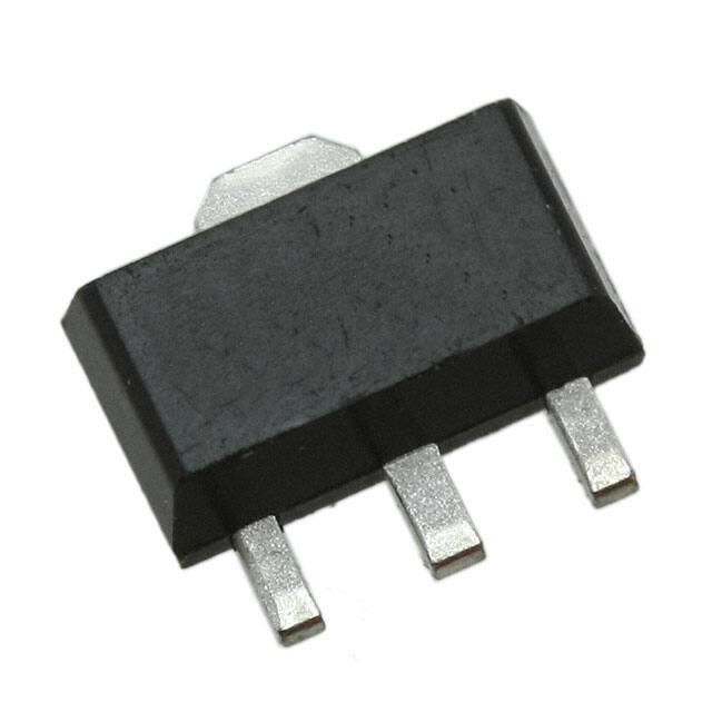
SOT−89
CASE 528AH
Features
•
•
•
•
•
•
•
•
1. Ref
2. Anode
3. Cathode
3
Programmable Output Voltage to 36 V
Low Dynamic Output Impedance: 0.2 W (Typical)
Sink Current Capability: 1.0 to 100 mA
Equivalent Full−Range Temperature Coefficient of 50 ppm/°C
(Typical)
Temperature Compensated for Operation Over Full Rated Operating
Temperature Range
Low Output Noise Voltage
Fast Turn−on Response
These Devices are Pb−Free, Halogen Free/BFR Free and are RoHS
Compliant
2
1
1. Cathode
2. Ref
3. Anode
SOT−23FL
CASE 318AB
3
1
2
SOT−23
CASE 318BM
M32
1. Ref
2. Cathode
3. Anode
M3
1. Cathode
2. Ref
3. Anode
ORDERING INFORMATION
Product Number
Output Voltage
Tolerance
Operating
Temperature
Top Mark(1)
Package
Shipping†
LM431SACMFX
2%
−25 to +85_C
Tape and Reel
43A □
SOT−23FL 3L
LM431SACM3X
43L ◎
SOT−23 3L
LM431SACM32X
43G ◎
SOT−23 3L
1%
43B
SOT−89 3L
LM431SBCMFX
LM431SBCMLX
43B □
SOT−23FL 3L
LM431SBCM3X
43M ◎
SOT−23 3L
43H ◎
SOT−23 3L
43C
SOT−89 3L
LM431SCCMFX
43C □
SOT−23FL 3L
LM431SCCM3X
43N ◎
SOT−23 3L
LM431SCCM32X
43J ◎
SOT−23 3L
43AI
SOT−23FL 3L
LM431SBCM32X
LM431SCCMLX
0.5%
−40 to +85_C
LM431SAIMFX
2%
LM431SBIMFX
1%
43BI
SOT−23FL 3L
LM431SCIMFX
0.5%
43CI
SOT−23FL 3L
†For information on tape and reel specifications, including part orientation and tape sizes, please refer to our Tape and Reel Packaging
Specification Brochure, BRD8011/D.
1. SOT−23 and SOT−23FL have basically four−character marking except LM431SAIMFX. (3 letters for device code + 1 letter for date code)
SOT−23FL date code is composed of 1 digit numeric or alphabetic week code adding bar−type year code.
© Semiconductor Components Industries, LLC, 2018
March, 2021 − Rev. 9
1
Publication Order Number:
LM431SA/D
�LM431SA, LM431SB, LM431SC
Block Diagram
Figure 1. Block Diagram
ABSOLUTE MAXIMUM RATINGS (TA = 25°C unless otherwise noted)
Symbol
Parameter
VKA
Cathode Voltage
IKA
Cathode current Range (Continuous)
IREF
Reference Input Current Range
RθJA
PD
TJ
Thermal Resistance Junction−Air (2, 3)
Power Dissipation (4, 5)
Value
Unit
37
V
−100 to +150
mA
−0.05 to +10.00
mA
ML Suffix Package (SOT−89)
220
°C/W
MF Suffix Package (SOT−23FL)
350
M32, M3 Suffix Package (SOT−23)
400
ML Suffix Package (SOT−89)
560
MF Suffix Package (SOT−23FL)
350
M32, M3 Suffix Package (SOT−23)
310
Junction Temperature
TOPR
Operating Temperature Range
TSTG
Storage Temperature Range
mW
150
°C
All products except LM431SAIMFX
−25 to +85
LM431SAIMFX, SBIMFX, SCIMFX
−40 to +85
°C
−65 to +150
°C
Stresses exceeding those listed in the Maximum Ratings table may damage the device. If any of these limits are exceeded, device functionality
should not be assumed, damage may occur and reliability may be affected.
2. Thermal resistance test board
Size: 1.6 mm x 76.2 mm x 114.3 mm (1S0P) JEDEC Standard: JESD51−3, JESD51−7.
3. Assume no ambient airflow.
4. TJMAX = 150°C; ratings apply to ambient temperature at 25°C.
5. Power dissipation calculation: PD = (TJ − TA) / RθJA.
RECOMMENDED OPERATING CONDITIONS
Symbol
Parameter
Min.
Max.
Unit
VKA
Cathode Voltage
VREF
36
V
IKA
Cathode Current
1
100
mA
Functional operation above the stresses listed in the Recommended Operating Ranges is not implied. Extended exposure to stresses beyond
the Recommended Operating Ranges limits may affect device reliability.
www.onsemi.com
2
�LM431SA, LM431SB, LM431SC
ELECTRICAL CHARACTERISTICS (Note 6, Values are at TA = 25°C unless otherwise noted)
LM431SA
Symbol
VREF
Parameter
Reference Input
Voltage
Min.
Conditions
VKA = VREF, IKA = 10 mA
DVREF /
DVKA
IREF
Reference Input
Current
Max.
Min.
Typ.
LM431SC
Max.
Min.
Typ.
Max.
2.450 2.500 2.550 2.470 2.495 2.520 2.482 2.495 2.508
SOT−89
Deviation of ReferSOT−23FL
VKA = VREF,
DVREF / DT ence Input Voltage I = 10 mA
KA
Over− TemperaTMIN ≤ TA ≤ TMAX SOT−23
ture
Ratio of Change in
Reference Input
Voltage to the
IKA =10 mA
Change in Cathode Voltage
Typ.
LM431SB
DVKA =
10 V−VREF
Unit
V
4.5
17.0
4.5
17.0
4.5
17.0
mV
6.6
24
6.6
24
6.6
24
mV
−1.0
−2.7
−1.0
−2.7
−1.0
−2.7
mV/V
DVKA =
36 V − 10 V
−0.5
−2.0
−0.5
−2.0
−0.5
−2.0
IKA = 10 mA, R1 = 10 KW, R2 = ∞
1.5
4.0
1.5
4.0
1.5
4.0
μA
Deviation of Refer- IKA = 10 mA,
SOT−89
SOT−23FL
0.4
1.2
0.4
1.2
0.4
1.2
μA
Over Full Temper- R2 = ∞,
ature Range
TA = Full Range
SOT−23
0.8
2.0
0.8
2.0
0.8
2.0
μA
DIREF / DT ence Input Current R1 = 10 KW,
IKA(MIN)
Minimum Cathode
Current for Regu- VKA = VREF
lation
0.45
1.00
0.45
1.00
0.45
1.00
mA
IKA(OFF)
Off −Stage Cathode Current
VKA = 36 V, VREF = 0
0.05
1.00
0.05
1.00
0.05
1.00
μA
VKA = VREF, IKA = 1 to 100 mA,
f ≥ 1.0 kHz
0.15
0.50
0.15
0.50
0.15
0.50
W
ZKA
Dynamic Impedance
Product parametric performance is indicated in the Electrical Characteristics for the listed test conditions, unless otherwise noted. Product
performance may not be indicated by the Electrical Characteristics if operated under different conditions.
6. LM431SAI, LM431SBI, LM431SCI: − TA(min) = −40_C, TA(max) = +85_C
All other pins: − TA(min) = −25_C, TA(max) = +85_C
www.onsemi.com
3
�LM431SA, LM431SB, LM431SC
ELECTRICAL CHARACTERISTICS (Continued) (Notes 7 and 8, Values are at TA = 25°C unless otherwise noted)
LM431SAI
Symbol
VREF
Parameter
Conditions
Reference Input
Voltage
VKA = VREF, IKA = 10 mA
Deviation of ReferVREF(dev) ence Input Voltage
Over−Temperature
DVREF /
DVKA
IREF
LM431SBI
LM431SCI
Min. Typ. Max. Min. Typ. Max. Min.
Typ.
Max.
2.450 2.500 2.550 2.470 2.495 2.520 2.482 2.495 2.508
VKA = VREF, IKA = 10 mA, TMIN ≤ TA ≤
TMAX
DVKA = 10 V−VREF
Ratio of Change in
Reference Input Voltage to Change in
Cathode Voltage
IKA = 10 mA
Reference Input
Current
IKA = 10 mA, R1 =10 KW, R2 = ∞
5
20
Unit
V
5
20
5
20
mV
−1.0 −2.7
−1.0
−2.7
−1.0
−2.7
−0.5 −2.0
−0.5
−2.0
−0.5
−2.0
1.5
4.0
1.5
4.0
1.5
4.0
μA
0.8
2.0
0.8
2.0
0.8
2.0
μA
mV/V
DVKA = 36 V − 10 V
Deviation of ReferIKA = 10 mA, R1 = 10 KW, R2 = ∞,
IREF(dev) ence Input Current
Over Full Temperature TMIN ≤ TA ≤ TMAX
Range
IKA(MIN)
Minimum Cathode
VKA = VREF
Current for Regulation
0.45 1.00
0.45
1.00
0.45
1.00
mA
IKA(OFF)
Off −Stage Cathode
Current
VKA = 36 V, VREF = 0
0.05 1.00
0.05
1.00
0.05
1.00
μA
ZKA
Dynamic Impedance
VKA = VREF, IKA = 1 to 100 mA,
f ≥ 1.0 kHz
0.15 0.50
0.15
0.50
0.15
0.50
W
7. LM431SAI, LM431SBI, LM431SCI: − TA(min) = −40_C, TA(max) = +85_C
All other pins: − TA(min) = −25_C, TA(max) = +85_C
8. The deviation parameters VREF(dev) and IREF(dev)are defined as the differences between the maximum and minimum values obtained over the
rated temperature range. The average full−range temperature coefficient of the reference input voltage, αVREF, is defined as:
ǒ Ǔ
ppm
|aV REF|
+
°C
ǒ
V REF(dev)
V
REF
Ǔ @ 10
(at 25°C)
6
where TMAX −TMIN is the rated operating free−air temperature range
of the device.
T MAX * T MIN
aVREF can be positive or negative, depending on whether minimum
VREF or maximum VREF, respectively, occurs at the lower
temperature.
VREF(min)
Example:
VREF(dev) = 4.5 mV, VREF = 2500 mV at 25°C,
TMAX −TMIN = 125°C for LM431SAI.
VREF(dev)
VREF(max)
|aV REF| +
TMAX -TMIN
ǒ
4.5 mV
2500 mV
Ǔ @ 10
125°C
6
+ 14.4 ppmń°C
Because minimum VREF occurs at the lower temperature, the
coefficient is positive.
www.onsemi.com
4
�LM431SA, LM431SB, LM431SC
TEST CIRCUITS
LM431S
LM431S
Figure 2. Test Circuit for VKA = VREF
Figure 3. Test Circuit for VKA . VREF
LM431S
Figure 4. Test Circuit for IKA(OFF)
www.onsemi.com
5
�LM431SA, LM431SB, LM431SC
TYPICAL APPLICATIONS
ǒ
VO + 1 )
Ǔ
ǒ
R1
V ref
R2
VO + 1 )
Ǔ
R1
V ref
R2
LM7805/MC7805
LM431S
LM431S
Figure 5. Shunt Regulator
ǒ
VO + 1 )
Figure 6. Output Control for Three−Terminal Fixed
Regulator
Ǔ
R1
V ref
R2
LM431S
Figure 7. High Current Shunt Regulator
LM431S
LM431S
Figure 9. Constant−Current Sink
Figure 8. Current Limit or Current Source
www.onsemi.com
6
�LM431SA, LM431SB, LM431SC
TYPICAL PERFORMANCE CHARACTERISTICS
800
TA = 25°C
100
50
0
−50
−100
−2
−1
VKA = VREF
IK − Cathode Current (mA)
VKA = VREF
IK, Cathode Current (mA)
IK − Cathode Current (mA)
150
0
1
2
600
200
0
0
0.20
3
3.5
Iref − Reference Input
Current (mA)
0.16
0.14
0.12
0.10
0.08
0.06
0.04
0.02
−25
0
25
50
75
100
125
3.0
2.5
2.0
1.5
1.0
0.5
0.0
−50
150
−25
0
25
50
75
100
125
TA − Ambient Temperature (°C)
o
, Ambient Temperature
C) (
TA −TAmbient
Temperature
(°C)
A
Figure 13. Reference Input Current vs. Ambient
Temperature
Figure 12. OFF−State Cathode Current vs. Ambient
Temperature
6
60
TA = 25°C
50
IKA = 10 mA
Voltage Swing (V)
Open Loop Voltage Gain (dB)
2
Figure 11. Cathode Current vs. Cathode Voltage
0.18
40
30
20
10
TA = 25°C
INPUT
5
4
3
OUTPUT
2
1
0
−10
1
VKA − Cathode Voltage (V)
Figure 10. Cathode Current vs. Cathode Voltage
Ioff − Off−State Cathode
Current (mA)
IKA(MIN)
400
−200
−1
3
VKA, Cathode Voltage (V)
VKA − Cathode Voltage (V)
0.00
−50
TA = 25°C
1k
10k
100k
Frequency (Hz)
1M
0
10M
Frequency (Hz)
0
4
8
12
16
Time (ms)
Figure 15. Pulse Response
Figure 14. Frequency vs. Small Signal Voltage
Amplification
www.onsemi.com
7
20
�LM431SA, LM431SB, LM431SC
5
4
A. VKA = Vref
120
B. VKA = 5.0 V @ IK = 10 mA
A
100
Current (mA)
IK − Cathode Current (mA)
140
TA = 25°C
80
60
40
3
2
1
20
B
0
100p
1n
10n
100n
1?
0
0.0
10?
0.2
0.4
0.6
0.8
1.0
1.2
1.4
1.6
1.8
2.0
Anode−Ref. Voltage(V)
Anode−Ref.
Voltage (V)
CL − Load Capacitance
Figure 17. Anode−Reference Diode Curve
Figure 16. Stability Boundary Conditions
5
2.51
Vref − Reference Input
Voltage (V)
Cu rrent(mA)
Current (mA)
4
3
2
1
0
0.0
0.2
0.4
0.6 0.8 1.0 1.2 1.4
Ref.−Cathode Voltage(V)
1.6
1.8
2.0
2.50
2.49
2.48
2.47
2.46
−50
Ref.−Cathode Voltage (V)
−25
0
25
50
75
100
125
TA − Ambient Temperature (°C)
Figure 18. Reference−Cathode Diode Curve
Figure 19. Reference Input Voltage vs. Ambient
Temperature
www.onsemi.com
8
�MECHANICAL CASE OUTLINE
PACKAGE DIMENSIONS
SOT23−FL3L
CASE 318AB
ISSUE O
DATE 11 DEC 2020
GENERIC
MARKING DIAGRAM*
XXXM
1
XXX = Specific Device Code
M = Date Code
DOCUMENT NUMBER:
DESCRIPTION:
98AON27911H
SOT23−FL3L
*This information is generic. Please refer to
device data sheet for actual part marking.
Pb−Free indicator, “G” or microdot “G”, may
or may not be present. Some products may
not follow the Generic Marking.
Electronic versions are uncontrolled except when accessed directly from the Document Repository.
Printed versions are uncontrolled except when stamped “CONTROLLED COPY” in red.
PAGE 1 OF 1
ON Semiconductor and
are trademarks of Semiconductor Components Industries, LLC dba ON Semiconductor or its subsidiaries in the United States and/or other countries.
ON Semiconductor reserves the right to make changes without further notice to any products herein. ON Semiconductor makes no warranty, representation or guarantee regarding
the suitability of its products for any particular purpose, nor does ON Semiconductor assume any liability arising out of the application or use of any product or circuit, and specifically
disclaims any and all liability, including without limitation special, consequential or incidental damages. ON Semiconductor does not convey any license under its patent rights nor the
rights of others.
© Semiconductor Components Industries, LLC, 2018
www.onsemi.com
�MECHANICAL CASE OUTLINE
PACKAGE DIMENSIONS
SOT−23
CASE 318BM
ISSUE O
DOCUMENT NUMBER:
DESCRIPTION:
98AON13784G
SOT−23
DATE 31 AUG 2016
Electronic versions are uncontrolled except when accessed directly from the Document Repository.
Printed versions are uncontrolled except when stamped “CONTROLLED COPY” in red.
PAGE 1 OF 1
ON Semiconductor and
are trademarks of Semiconductor Components Industries, LLC dba ON Semiconductor or its subsidiaries in the United States and/or other countries.
ON Semiconductor reserves the right to make changes without further notice to any products herein. ON Semiconductor makes no warranty, representation or guarantee regarding
the suitability of its products for any particular purpose, nor does ON Semiconductor assume any liability arising out of the application or use of any product or circuit, and specifically
disclaims any and all liability, including without limitation special, consequential or incidental damages. ON Semiconductor does not convey any license under its patent rights nor the
rights of others.
© Semiconductor Components Industries, LLC, 2019
www.onsemi.com
�MECHANICAL CASE OUTLINE
PACKAGE DIMENSIONS
SOT−89 3 LEAD
CASE 528AH
ISSUE O
1.87
1.45
4.50
3.90
4.70
4.30
C
DATE 31 AUG 2016
A
C
2.23 MIN
0.50 X 45
0.30 X 45
B
1.40
2.70
2.30
C
1
1.30
0.89
2
CL SYMM
5.30 MIN
C
90
3
2.00 MIN
0.52
(2X) C
0.30
0.10 M C A B
0.54
1.50
2
1
0.90 MIN 2X
3.00
1.70
1.30
C
3
0.96 MIN
1.50
3.00 MIN
LAND PATTERN
RECOMMENDATION
SEATING PLANE
C
0.35
0.60
0.40
3
C
0.50
0.35
1
2.29
2.13
2.70
NOTES: UNLESS OTHERWISE SPECIFIED.
A. REFERENCE TO JEDEC TO-243 VARIATION AA.
B. ALL DIMENSIONS ARE IN MILLIMETERS.
C DOES NOT COMPLY JEDEC STANDARD VALUE.
D. DIMENSIONS ARE EXCLUSIVE OF BURRS,
MOLD FLASH AND TIE BAR PROTRUSION.
E. DIMENSION AND TOLERANCE AS PER ASME
Y14.5−1994.
DOCUMENT NUMBER:
DESCRIPTION:
98AON13791G
SOT−89 3 LEAD
Electronic versions are uncontrolled except when accessed directly from the Document Repository.
Printed versions are uncontrolled except when stamped “CONTROLLED COPY” in red.
PAGE 1 OF 1
ON Semiconductor and
are trademarks of Semiconductor Components Industries, LLC dba ON Semiconductor or its subsidiaries in the United States and/or other countries.
ON Semiconductor reserves the right to make changes without further notice to any products herein. ON Semiconductor makes no warranty, representation or guarantee regarding
the suitability of its products for any particular purpose, nor does ON Semiconductor assume any liability arising out of the application or use of any product or circuit, and specifically
disclaims any and all liability, including without limitation special, consequential or incidental damages. ON Semiconductor does not convey any license under its patent rights nor the
rights of others.
© Semiconductor Components Industries, LLC, 2019
www.onsemi.com
�ON Semiconductor and
are trademarks of Semiconductor Components Industries, LLC dba ON Semiconductor or its subsidiaries in the United States and/or other countries.
ON Semiconductor owns the rights to a number of patents, trademarks, copyrights, trade secrets, and other intellectual property. A listing of ON Semiconductor’s product/patent
coverage may be accessed at www.onsemi.com/site/pdf/Patent−Marking.pdf. ON Semiconductor reserves the right to make changes without further notice to any products herein.
ON Semiconductor makes no warranty, representation or guarantee regarding the suitability of its products for any particular purpose, nor does ON Semiconductor assume any liability
arising out of the application or use of any product or circuit, and specifically disclaims any and all liability, including without limitation special, consequential or incidental damages.
Buyer is responsible for its products and applications using ON Semiconductor products, including compliance with all laws, regulations and safety requirements or standards,
regardless of any support or applications information provided by ON Semiconductor. “Typical” parameters which may be provided in ON Semiconductor data sheets and/or
specifications can and do vary in different applications and actual performance may vary over time. All operating parameters, including “Typicals” must be validated for each customer
application by customer’s technical experts. ON Semiconductor does not convey any license under its patent rights nor the rights of others. ON Semiconductor products are not
designed, intended, or authorized for use as a critical component in life support systems or any FDA Class 3 medical devices or medical devices with a same or similar classification
in a foreign jurisdiction or any devices intended for implantation in the human body. Should Buyer purchase or use ON Semiconductor products for any such unintended or unauthorized
application, Buyer shall indemnify and hold ON Semiconductor and its officers, employees, subsidiaries, affiliates, and distributors harmless against all claims, costs, damages, and
expenses, and reasonable attorney fees arising out of, directly or indirectly, any claim of personal injury or death associated with such unintended or unauthorized use, even if such
claim alleges that ON Semiconductor was negligent regarding the design or manufacture of the part. ON Semiconductor is an Equal Opportunity/Affirmative Action Employer. This
literature is subject to all applicable copyright laws and is not for resale in any manner.
PUBLICATION ORDERING INFORMATION
LITERATURE FULFILLMENT:
Email Requests to: orderlit@onsemi.com
ON Semiconductor Website: www.onsemi.com
◊
TECHNICAL SUPPORT
North American Technical Support:
Voice Mail: 1 800−282−9855 Toll Free USA/Canada
Phone: 011 421 33 790 2910
www.onsemi.com
1
Europe, Middle East and Africa Technical Support:
Phone: 00421 33 790 2910
For additional information, please contact your local Sales Representative
�