LMV821, LMV824
Single and Quad Low
Voltage, Rail-to-Rail
Operational Amplifiers
The LMV821 and LMV824 are operational amplifiers with low
input voltage offset and drift vs. temperature. In spite of low quiescent
current requirements these devices have 5 MHz bandwidth and 1.4
V/ms slew rate. In addition they provide rail−to−rail output swing into
600 W loads. The input common−mode voltage range includes
ground, and the maximum input offset voltage is only 3.5 mV.
Substantially large capacitive loads can be driven by simply adding a
pullup resistor or isolation resistor.
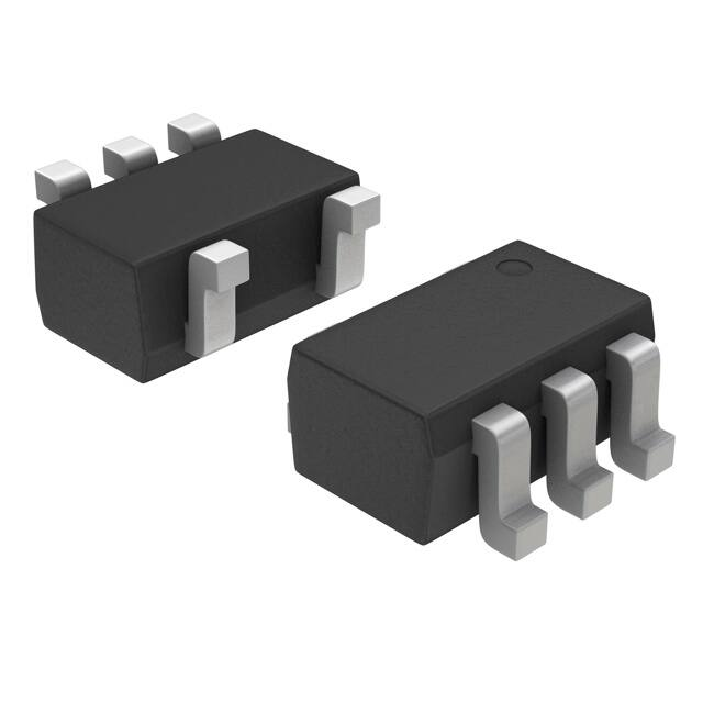
The LMV821 (single) is available in a space−saving SC70−5 while
the quad comes in SOIC and TSSOP packages.
www.onsemi.com
1
1
SOIC−14
CASE 751A
SC−70
CASE 419A
Features
•
•
•
•
•
•
•
Low Offset Voltage: 3.5 mV
Very low Offset Drift: 1.0 mV/°C
High Bandwidth: 5 MHz
Rail−to−Rail Output Swing into a 600 W load
Capable of driving highly capacitive loads
Small Packages:
LMV821 in SC−70
LMV824 in SOIC−14 and TSSOP−14
These Devices are Pb−Free and are RoHS Compliant
1
TSSOP−14
CASE 948G
ORDERING AND MARKING INFORMATION
See detailed ordering, marking and shipping information in the
package dimensions section on page 2 of this data sheet.
Typical Applications
• Notebook Computers
• PDAs
• Modem Transmitter/ Receivers
80
80
VS = 5 V, RL = 100 kW
70
70
60
CMRR (dB)
GAIN (dB)
50
40
30
20
60
VS = 5 V
50
10
40
0
−10
−20
1k
10k
100k
FREQUENCY (Hz)
1M
30
−1
10M
Figure 1. Gain vs. Frequency
© Semiconductor Components Industries, LLC, 2015
May, 2015 − Rev. 3
0
1
2
3
4
INPUT COMMON MODE VOLTAGE (V)
5
Figure 2. CMRR vs. Input Common Mode
Voltage
1
Publication Order Number:
LMV821/D
�LMV821, LMV824
MARKING DIAGRAMS
SC−70
SOIC−14
TSSOP−14
14
14
LMV
824
ALYWG
G
LMV824G
AWLYWW
AAEMG
G
1
AAE
M
G
= Specific Device Code
= Date Code
= Pb−Free Package
(Note: Microdot may be in either location)
1
LMV824 = Specific Device Code
A
= Assembly Location
WL
= Wafer Lot
Y
= Year
WW
= Work Week
G
= Pb−Free Package
LMV824 = Specific Device Code
A
= Assembly Location
L
= Wafer Lot
Y
= Year
W
= Work Week
G
= Pb−Free Package
(Note: Microdot may be in either location)
PIN CONNECTIONS
SC70−5
1
IN A−
2
V+
+IN
2
+
−
V−
IN A+
V+
3
4
1
IN A−
2
3
12 IN D+
IN A+
3
12 IN D+
4
11 V−
V+
4
11 V−
IN B+
5
10 IN C+
IN B+
5
10 IN C+
IN B−
6
9
IN C−
IN B−
6
OUT B
7
8
OUT C
OUT B
7
D
+ −
OUTPUT
+ −
(Top View)
14 OUT D
OUT A
A
− +
− +
−IN
14 OUT D
13 IN D−
5
B
C
(Top View)
A
− +
D
+ −
+ −
OUT A
TSSOP−14
− +
1
SOIC−14
B
C
13 IN D−
9
IN C−
8
OUT C
(Top View)
ORDERING INFORMATION
Number of
Channels
Specific Device Marking
Package Type
Shipping†
LMV821SQ3T2G
Single
AAE
SC−70
(Pb−Free)
3000 / Tape & Reel
LMV824DR2G
Quad
LMV824
SOIC−14
(Pb−Free)
2500 / Tape & Reel
LMV824DTBR2G
Quad
LMV
824
TSSOP−14
(Pb−Free)
2500 / Tape & Reel
Order Number
†For information on tape and reel specifications, including part orientation and tape sizes, please refer to our Tape and Reel Packaging
Specifications Brochure, BRD8011/D.
www.onsemi.com
2
�LMV821, LMV824
MAXIMUM RATINGS
Symbol
VS
Rating
Supply Voltage (Operating Range VS = 2.7 V to 5.5 V)
Value
Unit
5.5
V
VIDR
Input Differential Voltage
$Supply Voltage
V
VICR
Input Common Mode Voltage Range
−0.5 to (V+) +0.5
V
10
mA
Maximum Input Current
tSO
Output Short Circuit (Note 1)
TJ
Maximum Junction Temperature (Operating Range −40°C to 85°C)
qJA
Thermal Resistance
TSTG
VESD
Continuous
150
°C
°C/W
SC−70
280
SOIC−14
156
TSSOP−14
190
−65 to 150
°C
Mounting Temperature (Infrared or Convection − 20 sec)
235
°C
ESD Tolerance
200
2000
V
Storage Temperature
Machine Model
Human Body Model
Stresses exceeding those listed in the Maximum Ratings table may damage the device. If any of these limits are exceeded, device functionality
should not be assumed, damage may occur and reliability may be affected.
1. Continuous short−circuit operation to ground at elevated ambient temperature can result in exceeding the maximum allowed junction temperature of 150°C. Output currents in excess of 45 mA over long term may adversely affect reliability. Shorting output to either V+ or V−
will adversely affect reliability.
www.onsemi.com
3
�LMV821, LMV824
2.7V DC ELECTRICAL CHARACTERISTICS Unless otherwise noted, all min/max limits are guaranteed for TA = 25°C, V+ = 2.7 V,
V− = 0 V, VCM = V+/2, VO = V+/2 and RL > 1 MW. Typical specifications represent the most likely parametric norm. Min/Max
specifications are guaranteed by testing, characterization, or statistical analysis.
Parameter
Input Offset Voltage
Symbol
Conditions
Min
VIO
Typ
Max
Unit
1
3.5
mV
TA = −40°C to +85°C
Input Offset Voltage Average
Drift
Input Bias Current
4
TCVOS
IB
105
TA = −40°C to +85°C
Input Offset Current
0.5
TA = −40°C to +85°C
70
TA = −40°C to +85°C
68
1.5 V v V+ v 4 V, V − = −1 V, VO = 0 V,
VCM = 0.0 V
75
TA = −40°C to +85°C
70
VCM
For CMRR w 53 dB
and TA = −40°C to +85°C
−0.2
−0.3 to
2.0
AV
RL = 600 W, VO = 0.5 V to 2.5 V
80
95
TA = −40°C to +85°C
70
RL = 2 kW, VO = 0.5 V to 2.5 V
83
TA = −40°C to +85°C
80
RL = 600 W to 1.35 V
2.5
TA = −40°C to +85°C
2.4
Power Supply Rejection Ratio
PSRR
Input Common−Mode Voltage
Range
Large Signal Voltage Gain
Output Swing
VOH
VOL
VOL
Supply Current
IO
ICC
RL = 600 W to 1.35 V
85
dB
2.6
2.5
12
Sinking, VO = 2.7 V
12
0.21
2.66
0.12
mA
26
0.242
TA = −40°C to +85°C
4
V
0.2
Sourcing, VO = 0 V
www.onsemi.com
dB
2.58
0.08
RL = 2 kW to 1.35 V
TA = −40°C to +85°C
V
0.3
RL = 2 kW to 1.35 V
LMV824 (All Four Channels)
1.9
89
0.13
TA = −40°C to +85°C
LMV821 (Single)
nA
dB
TA = −40°C to +85°C
Output Current
30
85
TA = −40°C to +85°C
VOH
nA
50
0 V v VCM v 1.7 V
CMRR
210
315
IIO
Common−Mode Rejection
Ratio
mV/°C
1
0.3
0.5
1
1.3
1.5
mA
�LMV821, LMV824
2.5V DC ELECTRICAL CHARACTERISTICS Unless otherwise noted, all min/max limits are guaranteed for TA = 25°C, V+ = 2.5 V,
V− = 0 V, VCM = V+/2, VO = V+/2 and RL > 1 MW. Typical specifications represent the most likely parametric norm. Min/Max
specifications are guaranteed by testing, characterization, or statistical analysis.
Parameter
Input Offset Voltage
Symbol
Conditions
VIO
TA = −40°C to +85°C
Min
Typ
Max
Unit
1
3.5
mV
4
Output Swing
VOH
VOL
RL = 600 W to 1.25 V
2.3
TA = −40°C to +85°C
2.2
RL = 600 W to 1.25 V
0.13
TA = −40°C to +85°C
VOH
VOL
V
2.37
0.20
0.3
RL = 2 kW to 1.25 V
2.4
TA = −40°C to +85°C
2.3
2.46
0.08
RL = 2 kW to 1.25 V
TA = −40°C to +85°C
0.12
0.20
2.7V AC ELECTRICAL CHARACTERISTICS Unless otherwise specified, all limits are guaranteed for TA = 25°C, V+ = 2.7 V, V− =
0 V, VCM = 1.0 V, VO = V+/2 and RL > 1 MW. Typical specifications represent the most likely parametric norm. Min/Max specifications are
guaranteed by testing, characterization, or statistical analysis.
Parameter
Slew Rate
Symbol
Conditions
SR
(Note 2)
Min
Typ
Max
Unit
1.5
V/uS
GBWP
5
MHz
Phase Margin
qm
55
°
Gain Margin
Gm
12.9
dB
Input−Referred Voltage Noise
en
f = 1 kHz, VCM = 1 V
12
nV/√Hz
Input−Referred Current Noise
in
f = 1kHz
0.2
pA/√Hz
THD
f = 1 kHz, AV = −2, RL = 10 kW , VO = 1.8 VPP
0.023
%
(Note 3)
135
dB
Gain Bandwidth Product
Total Harmonic Distortion
Amplifier−to−Amplifier Isolation
2. Connected as voltage follower with input step from 0.5 V to 1.5 V. Number specified is the average of the positive and negative slew rates.
3. Input referred, RL = 100 kW connected to V+/2. Each amp excited in turn with 1kHz to produce VO = 3 VPP. For Supply Voltages < 3 V,
VO = V+.
www.onsemi.com
5
�LMV821, LMV824
5V DC ELECTRICAL CHARACTERISTICS Unless otherwise noted, all min/max limits are guaranteed for TA = 25°C, V+ = 5 V,V−
= 0 V, VCM = V+/2, VO = V+/2 and RL > 1 MW. Typical specifications represent the most likely parametric norm. Min/Max specifications
are guaranteed by testing, characterization, or statistical analysis.
Parameter
Input Offset Voltage
Symbol
Conditions
Min
VIO
Typ
Max
Unit
1
3.5
mV
TA = −40°C to +85°C
Input Offset Voltage Average
Drift
Input Bias Current
4
TCVOS
IB
119
TA = −40°C to +85°C
Input Offset Current
0.5
TA = −40°C to +85°C
72
TA = −40°C to +85°C
70
1.7 V v V+ v 4 V, V − = 1 V, VO = 0 V,
VCM = 0.0 V
75
TA = −40°C to +85°C
70
VCM
For CMRR w 58 dB
and TA = − 40°C to +85°C
−0.2
−0.2 to
4.3
AV
RL = 600 W, VO = 1.0 V to 4.0 V
87
100
TA = −40°C to +85°C
73
RL = 2 kW, VO = 1.0 V to 4.0 V
84
TA = −40°C to +85°C
82
RL = 600 W to 2.5 V
4.75
TA = −40°C to +85°C
4.7
Power Supply Rejection Ratio
PSRR
Input Common−Mode Voltage
Range
Large Signal Voltage Gain
Output Swing
VOH
VOL
VOL
Supply Current
IO
RL = 600 W to 2.5 V
85
dB
4.85
4.8
20
TA = −40°C to +85°C
10
Sinking, Vo = 5 V
20
TA = −40°C to +85°C
15
0.15
mA
45
40
TA = −40°C to +85°C
0.4
0.6
0.5
TA = −40°C to +85°C
6
0.33
4.9
0.3
www.onsemi.com
V
0.2
Sourcing, Vo = 0 V
TA = −40°C to +85°C
dB
4.84
0.1
RL = 2 kW to 2.5 V
LMV824 (All Four Applications)
V
0.4
RL = 2 kW to 2.5 V
LMV822 (Both Applications)
4.2
99
0.17
TA = −40°C to +85°C
ICC
nA
dB
TA = −40°C to +85°C
Output Current
30
90
TA = −40°C to +85°C
VOH
nA
50
0 V v VCM v 4.0 V
CMRR
245
380
IIO
Common−Mode Rejection
Ratio
mV/°C
1
0.7
0.9
1
1.3
1.5
mA
�LMV821, LMV824
5V AC ELECTRICAL CHARACTERISTICS Unless otherwise specified, all limits are guaranteed for TA = 25°C, V+ = 5 V, V− = 0 V,
VCM = 2.0 V, VO = V+/2 and RL > 1 MW. Typical specifications represent the most likely parametric norm. Min/Max specifications are
guaranteed by testing, characterization, or statistical analysis.
Parameter
Slew Rate
Symbol
Conditions
SR
(Note 4)
Min
Typ
Max
Unit
2
V/mS
GBWP
5.6
MHz
Phase Margin
qm
63
°
Gain Margin
Gm
11.7
dB
Input−Referred Voltage Noise
en
f = 1 kHz, VCM = 1 V
11
nV/√Hz
Input−Referred Current Noise
in
f = 1 kHz
0.21
pA/√Hz
THD
f = 1 kHz, AV = −2, RL = 10 kW , VO = 4.11 VPP
0.012
%
(Note 5)
135
dB
Gain Bandwidth Product
Total Harmonic Distortion
Amplifier−to−Amplifier Isolation
4. Connected as voltage follower with input step from 0.5 V to 3.5 V. Number specified is the average of the positive and negative slew rates.
5. Input referred, RL = 100 kW connected to V+/2. Each amp excited in turn with 1 kHz to produce VO = 3 VPP. (For Supply Voltages < 3 V,
VO = V+).
www.onsemi.com
7
�LMV821, LMV824
TYPICAL PERFORMANCE CHARACTERISTICS
100
90
100
70
+PSRR (dB)
80
60
40
VS = 2.7 V
60
50
40
30
20
20
10
0
100
1k
10k
0
100
100k
1k
10k
100k
FREQUENCY (Hz)
FREQUENCY (Hz)
Figure 3. Crosstalk Rejection vs. Frequency
Figure 4. +PSRR vs. Frequency
100
80
90
70
80
60
70
−PSRR (dB)
VS = 5 V
80
VS = 2.7 V
50
40
30
VS = 5 V, CL = 0 pF, RL = 100 kW
40
30
20
10
20
0
10
−10
0
100
1k
10k
100k
−20
1M
1k
10k
100k
1M
FREQUENCY (Hz)
FREQUENCY (Hz)
Figure 5. −PSRR vs. Frequency
Figure 6. Gain vs. Frequency
80
VS = 2.7 V, CL = 0 pF, RL = 100 kW
70
60
GAIN (dB)
50
40
30
20
10
0
−10
−20
1M
50
VS = 5 V
60
GAIN (dB)
CROSSTALK REJECTION (dB)
120
1k
10k
100k
1M
10M
FREQUENCY (Hz)
Figure 7. Gain vs. Frequency
Figure 8. Non−Inverting Stability vs.
Capacitive Load
www.onsemi.com
8
10M
�LMV821, LMV824
TYPICAL PERFORMANCE CHARACTERISTICS
3
AV = 1, RL = 100 kW, TA = 25°C
2.5
GAIN (dB)
SR+
2
1.5
SR−
1
0.5
2.5
3
3.5
4
4.5
5
FREQUENCY (Hz)
Figure 9. Gain vs. Frequency
Figure 10. Non−Inverting Large Signal Step
Response
Figure 11. Non−Inverting Small Signal Step
Response
Figure 12. Inverting Large Signal Step
Response
Figure 13. Inverting Small Signal Step
Response
www.onsemi.com
9
�LMV821, LMV824
APPLICATIONS INFORMATION
50 k
R1
5.0 k
VCC
VCC
R2
10 k
MC1403
VO
LMV821
VO
LMV821
VCC
−
Vref
−
+
+
fO +
1
V ref + V CC
2
2.5 V
R
R1
V O + 2.5 V(1 )
)
R2
R
Figure 14. Voltage Reference
C
C
1
2pRC
For: fo = 1.0 kHz
R = 16 kW
C = 0.01 mF
Figure 15. Wien Bridge Oscillator
VCC
C
R1
R3
C
−
Vin
R2
CO
VO
LMV821
Hysteresis
R2
VOH
R1
+
Vref
VO
Vref
+
Vin
LMV821
−
VO
VOL
CO = 10 C
VinL
Given: fo = center frequency
A(fo) = gain at center frequency
VinH
Choose value fo, C
Q
Then : R3 +
pf O C
Vref
R1
(V OL * V ref) ) V ref
R1 ) R2
R1
V inH +
(V OH * V ref) ) V ref
R1 ) R2
R1
H+
(V OH * V OL)
R1 ) R2
V inL +
R1 +
R2 +
R3
2 A(f O)
R1 R3
4Q 2 R1 * R3
Figure 16. Comparator with Hysteresis
For less than 10% error from operational amplifier,
((QO fO)/BW) < 0.1 where fo and BW are expressed in Hz.
If source impedance varies, filter may be preceded with
voltage follower buffer to stabilize filter parameters.
Figure 17. Multiple Feedback Bandpass Filter
www.onsemi.com
10
�MECHANICAL CASE OUTLINE
PACKAGE DIMENSIONS
SC−88A (SC−70−5/SOT−353)
CASE 419A−02
ISSUE L
SCALE 2:1
A
NOTES:
1. DIMENSIONING AND TOLERANCING
PER ANSI Y14.5M, 1982.
2. CONTROLLING DIMENSION: INCH.
3. 419A−01 OBSOLETE. NEW STANDARD
419A−02.
4. DIMENSIONS A AND B DO NOT INCLUDE
MOLD FLASH, PROTRUSIONS, OR GATE
BURRS.
G
5
4
−B−
S
1
2
DATE 17 JAN 2013
DIM
A
B
C
D
G
H
J
K
N
S
3
D 5 PL
0.2 (0.008)
B
M
M
N
INCHES
MIN
MAX
0.071
0.087
0.045
0.053
0.031
0.043
0.004
0.012
0.026 BSC
--0.004
0.004
0.010
0.004
0.012
0.008 REF
0.079
0.087
MILLIMETERS
MIN
MAX
1.80
2.20
1.15
1.35
0.80
1.10
0.10
0.30
0.65 BSC
--0.10
0.10
0.25
0.10
0.30
0.20 REF
2.00
2.20
J
GENERIC MARKING
DIAGRAM*
C
K
H
XXXMG
G
SOLDER FOOTPRINT
0.50
0.0197
XXX = Specific Device Code
M
= Date Code
G
= Pb−Free Package
0.65
0.025
0.65
0.025
0.40
0.0157
1.9
0.0748
SCALE 20:1
(Note: Microdot may be in either location)
*This information is generic. Please refer to
device data sheet for actual part marking.
Pb−Free indicator, “G” or microdot “G”, may
or may not be present. Some products may
not follow the Generic Marking.
mm Ǔ
ǒinches
STYLE 1:
PIN 1. BASE
2. EMITTER
3. BASE
4. COLLECTOR
5. COLLECTOR
STYLE 2:
PIN 1. ANODE
2. EMITTER
3. BASE
4. COLLECTOR
5. CATHODE
STYLE 3:
PIN 1. ANODE 1
2. N/C
3. ANODE 2
4. CATHODE 2
5. CATHODE 1
STYLE 4:
PIN 1. SOURCE 1
2. DRAIN 1/2
3. SOURCE 1
4. GATE 1
5. GATE 2
STYLE 6:
PIN 1. EMITTER 2
2. BASE 2
3. EMITTER 1
4. COLLECTOR
5. COLLECTOR 2/BASE 1
STYLE 7:
PIN 1. BASE
2. EMITTER
3. BASE
4. COLLECTOR
5. COLLECTOR
STYLE 8:
PIN 1. CATHODE
2. COLLECTOR
3. N/C
4. BASE
5. EMITTER
STYLE 9:
PIN 1. ANODE
2. CATHODE
3. ANODE
4. ANODE
5. ANODE
DOCUMENT NUMBER:
DESCRIPTION:
98ASB42984B
STYLE 5:
PIN 1. CATHODE
2. COMMON ANODE
3. CATHODE 2
4. CATHODE 3
5. CATHODE 4
Note: Please refer to datasheet for
style callout. If style type is not called
out in the datasheet refer to the device
datasheet pinout or pin assignment.
Electronic versions are uncontrolled except when accessed directly from the Document Repository.
Printed versions are uncontrolled except when stamped “CONTROLLED COPY” in red.
SC−88A (SC−70−5/SOT−353)
PAGE 1 OF 1
ON Semiconductor and
are trademarks of Semiconductor Components Industries, LLC dba ON Semiconductor or its subsidiaries in the United States and/or other countries.
ON Semiconductor reserves the right to make changes without further notice to any products herein. ON Semiconductor makes no warranty, representation or guarantee regarding
the suitability of its products for any particular purpose, nor does ON Semiconductor assume any liability arising out of the application or use of any product or circuit, and specifically
disclaims any and all liability, including without limitation special, consequential or incidental damages. ON Semiconductor does not convey any license under its patent rights nor the
rights of others.
© Semiconductor Components Industries, LLC, 2018
www.onsemi.com
�MECHANICAL CASE OUTLINE
PACKAGE DIMENSIONS
SOIC−14 NB
CASE 751A−03
ISSUE L
14
1
SCALE 1:1
D
DATE 03 FEB 2016
A
B
14
8
A3
E
H
L
1
0.25
B
M
DETAIL A
7
13X
M
b
0.25
M
C A
S
B
S
0.10
X 45 _
M
A1
e
DETAIL A
h
A
C
SEATING
PLANE
DIM
A
A1
A3
b
D
E
e
H
h
L
M
MILLIMETERS
MIN
MAX
1.35
1.75
0.10
0.25
0.19
0.25
0.35
0.49
8.55
8.75
3.80
4.00
1.27 BSC
5.80
6.20
0.25
0.50
0.40
1.25
0_
7_
INCHES
MIN
MAX
0.054 0.068
0.004 0.010
0.008 0.010
0.014 0.019
0.337 0.344
0.150 0.157
0.050 BSC
0.228 0.244
0.010 0.019
0.016 0.049
0_
7_
GENERIC
MARKING DIAGRAM*
SOLDERING FOOTPRINT*
6.50
NOTES:
1. DIMENSIONING AND TOLERANCING PER
ASME Y14.5M, 1994.
2. CONTROLLING DIMENSION: MILLIMETERS.
3. DIMENSION b DOES NOT INCLUDE DAMBAR
PROTRUSION. ALLOWABLE PROTRUSION
SHALL BE 0.13 TOTAL IN EXCESS OF AT
MAXIMUM MATERIAL CONDITION.
4. DIMENSIONS D AND E DO NOT INCLUDE
MOLD PROTRUSIONS.
5. MAXIMUM MOLD PROTRUSION 0.15 PER
SIDE.
14
14X
1.18
XXXXXXXXXG
AWLYWW
1
1
1.27
PITCH
XXXXX
A
WL
Y
WW
G
= Specific Device Code
= Assembly Location
= Wafer Lot
= Year
= Work Week
= Pb−Free Package
*This information is generic. Please refer to
device data sheet for actual part marking.
Pb−Free indicator, “G” or microdot “G”, may
or may not be present. Some products may
not follow the Generic Marking.
14X
0.58
DIMENSIONS: MILLIMETERS
*For additional information on our Pb−Free strategy and soldering
details, please download the ON Semiconductor Soldering and
Mounting Techniques Reference Manual, SOLDERRM/D.
STYLES ON PAGE 2
DOCUMENT NUMBER:
DESCRIPTION:
98ASB42565B
SOIC−14 NB
Electronic versions are uncontrolled except when accessed directly from the Document Repository.
Printed versions are uncontrolled except when stamped “CONTROLLED COPY” in red.
PAGE 1 OF 2
onsemi and
are trademarks of Semiconductor Components Industries, LLC dba onsemi or its subsidiaries in the United States and/or other countries. onsemi reserves
the right to make changes without further notice to any products herein. onsemi makes no warranty, representation or guarantee regarding the suitability of its products for any particular
purpose, nor does onsemi assume any liability arising out of the application or use of any product or circuit, and specifically disclaims any and all liability, including without limitation
special, consequential or incidental damages. onsemi does not convey any license under its patent rights nor the rights of others.
© Semiconductor Components Industries, LLC, 2019
www.onsemi.com
�SOIC−14
CASE 751A−03
ISSUE L
DATE 03 FEB 2016
STYLE 1:
PIN 1. COMMON CATHODE
2. ANODE/CATHODE
3. ANODE/CATHODE
4. NO CONNECTION
5. ANODE/CATHODE
6. NO CONNECTION
7. ANODE/CATHODE
8. ANODE/CATHODE
9. ANODE/CATHODE
10. NO CONNECTION
11. ANODE/CATHODE
12. ANODE/CATHODE
13. NO CONNECTION
14. COMMON ANODE
STYLE 2:
CANCELLED
STYLE 3:
PIN 1. NO CONNECTION
2. ANODE
3. ANODE
4. NO CONNECTION
5. ANODE
6. NO CONNECTION
7. ANODE
8. ANODE
9. ANODE
10. NO CONNECTION
11. ANODE
12. ANODE
13. NO CONNECTION
14. COMMON CATHODE
STYLE 4:
PIN 1. NO CONNECTION
2. CATHODE
3. CATHODE
4. NO CONNECTION
5. CATHODE
6. NO CONNECTION
7. CATHODE
8. CATHODE
9. CATHODE
10. NO CONNECTION
11. CATHODE
12. CATHODE
13. NO CONNECTION
14. COMMON ANODE
STYLE 5:
PIN 1. COMMON CATHODE
2. ANODE/CATHODE
3. ANODE/CATHODE
4. ANODE/CATHODE
5. ANODE/CATHODE
6. NO CONNECTION
7. COMMON ANODE
8. COMMON CATHODE
9. ANODE/CATHODE
10. ANODE/CATHODE
11. ANODE/CATHODE
12. ANODE/CATHODE
13. NO CONNECTION
14. COMMON ANODE
STYLE 6:
PIN 1. CATHODE
2. CATHODE
3. CATHODE
4. CATHODE
5. CATHODE
6. CATHODE
7. CATHODE
8. ANODE
9. ANODE
10. ANODE
11. ANODE
12. ANODE
13. ANODE
14. ANODE
STYLE 7:
PIN 1. ANODE/CATHODE
2. COMMON ANODE
3. COMMON CATHODE
4. ANODE/CATHODE
5. ANODE/CATHODE
6. ANODE/CATHODE
7. ANODE/CATHODE
8. ANODE/CATHODE
9. ANODE/CATHODE
10. ANODE/CATHODE
11. COMMON CATHODE
12. COMMON ANODE
13. ANODE/CATHODE
14. ANODE/CATHODE
STYLE 8:
PIN 1. COMMON CATHODE
2. ANODE/CATHODE
3. ANODE/CATHODE
4. NO CONNECTION
5. ANODE/CATHODE
6. ANODE/CATHODE
7. COMMON ANODE
8. COMMON ANODE
9. ANODE/CATHODE
10. ANODE/CATHODE
11. NO CONNECTION
12. ANODE/CATHODE
13. ANODE/CATHODE
14. COMMON CATHODE
DOCUMENT NUMBER:
DESCRIPTION:
98ASB42565B
SOIC−14 NB
Electronic versions are uncontrolled except when accessed directly from the Document Repository.
Printed versions are uncontrolled except when stamped “CONTROLLED COPY” in red.
PAGE 2 OF 2
onsemi and
are trademarks of Semiconductor Components Industries, LLC dba onsemi or its subsidiaries in the United States and/or other countries. onsemi reserves
the right to make changes without further notice to any products herein. onsemi makes no warranty, representation or guarantee regarding the suitability of its products for any particular
purpose, nor does onsemi assume any liability arising out of the application or use of any product or circuit, and specifically disclaims any and all liability, including without limitation
special, consequential or incidental damages. onsemi does not convey any license under its patent rights nor the rights of others.
© Semiconductor Components Industries, LLC, 2019
www.onsemi.com
�MECHANICAL CASE OUTLINE
PACKAGE DIMENSIONS
TSSOP−14 WB
CASE 948G
ISSUE C
14
DATE 17 FEB 2016
1
SCALE 2:1
14X K REF
0.10 (0.004)
0.15 (0.006) T U
M
T U
V
S
S
S
N
2X
14
L/2
0.25 (0.010)
8
M
B
−U−
L
PIN 1
IDENT.
N
F
7
1
0.15 (0.006) T U
NOTES:
1. DIMENSIONING AND TOLERANCING PER
ANSI Y14.5M, 1982.
2. CONTROLLING DIMENSION: MILLIMETER.
3. DIMENSION A DOES NOT INCLUDE MOLD
FLASH, PROTRUSIONS OR GATE BURRS.
MOLD FLASH OR GATE BURRS SHALL NOT
EXCEED 0.15 (0.006) PER SIDE.
4. DIMENSION B DOES NOT INCLUDE
INTERLEAD FLASH OR PROTRUSION.
INTERLEAD FLASH OR PROTRUSION SHALL
NOT EXCEED 0.25 (0.010) PER SIDE.
5. DIMENSION K DOES NOT INCLUDE DAMBAR
PROTRUSION. ALLOWABLE DAMBAR
PROTRUSION SHALL BE 0.08 (0.003) TOTAL
IN EXCESS OF THE K DIMENSION AT
MAXIMUM MATERIAL CONDITION.
6. TERMINAL NUMBERS ARE SHOWN FOR
REFERENCE ONLY.
7. DIMENSION A AND B ARE TO BE
DETERMINED AT DATUM PLANE −W−.
S
DETAIL E
K
A
−V−
K1
J J1
ÉÉÉ
ÇÇÇ
ÇÇÇ
ÉÉÉ
SECTION N−N
−W−
C
0.10 (0.004)
−T− SEATING
PLANE
H
G
D
DETAIL E
DIM
A
B
C
D
F
G
H
J
J1
K
K1
L
M
MILLIMETERS
INCHES
MIN
MAX
MIN MAX
4.90
5.10 0.193 0.200
4.30
4.50 0.169 0.177
−−−
1.20
−−− 0.047
0.05
0.15 0.002 0.006
0.50
0.75 0.020 0.030
0.65 BSC
0.026 BSC
0.50
0.60 0.020 0.024
0.09
0.20 0.004 0.008
0.09
0.16 0.004 0.006
0.19
0.30 0.007 0.012
0.19
0.25 0.007 0.010
6.40 BSC
0.252 BSC
0_
8_
0_
8_
GENERIC
MARKING DIAGRAM*
14
SOLDERING FOOTPRINT
XXXX
XXXX
ALYWG
G
7.06
1
1
0.65
PITCH
14X
0.36
14X
1.26
DIMENSIONS: MILLIMETERS
DOCUMENT NUMBER:
98ASH70246A
DESCRIPTION:
TSSOP−14 WB
A
L
Y
W
G
= Assembly Location
= Wafer Lot
= Year
= Work Week
= Pb−Free Package
(Note: Microdot may be in either location)
*This information is generic. Please refer to
device data sheet for actual part marking.
Pb−Free indicator, “G” or microdot “G”, may
or may not be present. Some products may
not follow the Generic Marking.
Electronic versions are uncontrolled except when accessed directly from the Document Repository.
Printed versions are uncontrolled except when stamped “CONTROLLED COPY” in red.
PAGE 1 OF 1
onsemi and
are trademarks of Semiconductor Components Industries, LLC dba onsemi or its subsidiaries in the United States and/or other countries. onsemi reserves
the right to make changes without further notice to any products herein. onsemi makes no warranty, representation or guarantee regarding the suitability of its products for any particular
purpose, nor does onsemi assume any liability arising out of the application or use of any product or circuit, and specifically disclaims any and all liability, including without limitation
special, consequential or incidental damages. onsemi does not convey any license under its patent rights nor the rights of others.
© Semiconductor Components Industries, LLC, 2019
www.onsemi.com
�onsemi,
, and other names, marks, and brands are registered and/or common law trademarks of Semiconductor Components Industries, LLC dba “onsemi” or its affiliates
and/or subsidiaries in the United States and/or other countries. onsemi owns the rights to a number of patents, trademarks, copyrights, trade secrets, and other intellectual property.
A listing of onsemi’s product/patent coverage may be accessed at www.onsemi.com/site/pdf/Patent−Marking.pdf. onsemi reserves the right to make changes at any time to any
products or information herein, without notice. The information herein is provided “as−is” and onsemi makes no warranty, representation or guarantee regarding the accuracy of the
information, product features, availability, functionality, or suitability of its products for any particular purpose, nor does onsemi assume any liability arising out of the application or use
of any product or circuit, and specifically disclaims any and all liability, including without limitation special, consequential or incidental damages. Buyer is responsible for its products
and applications using onsemi products, including compliance with all laws, regulations and safety requirements or standards, regardless of any support or applications information
provided by onsemi. “Typical” parameters which may be provided in onsemi data sheets and/or specifications can and do vary in different applications and actual performance may
vary over time. All operating parameters, including “Typicals” must be validated for each customer application by customer’s technical experts. onsemi does not convey any license
under any of its intellectual property rights nor the rights of others. onsemi products are not designed, intended, or authorized for use as a critical component in life support systems
or any FDA Class 3 medical devices or medical devices with a same or similar classification in a foreign jurisdiction or any devices intended for implantation in the human body. Should
Buyer purchase or use onsemi products for any such unintended or unauthorized application, Buyer shall indemnify and hold onsemi and its officers, employees, subsidiaries, affiliates,
and distributors harmless against all claims, costs, damages, and expenses, and reasonable attorney fees arising out of, directly or indirectly, any claim of personal injury or death
associated with such unintended or unauthorized use, even if such claim alleges that onsemi was negligent regarding the design or manufacture of the part. onsemi is an Equal
Opportunity/Affirmative Action Employer. This literature is subject to all applicable copyright laws and is not for resale in any manner.
PUBLICATION ORDERING INFORMATION
LITERATURE FULFILLMENT:
Email Requests to: orderlit@onsemi.com
onsemi Website: www.onsemi.com
◊
TECHNICAL SUPPORT
North American Technical Support:
Voice Mail: 1 800−282−9855 Toll Free USA/Canada
Phone: 011 421 33 790 2910
Europe, Middle East and Africa Technical Support:
Phone: 00421 33 790 2910
For additional information, please contact your local Sales Representative
�