Ordering number : ENA2184B
LV52204MT
Bi-CMOS IC
LED Boost Driver with PWM
and 1-Wire Dimming
http://onsemi.com
Overview
The LV52204MT is a high voltage boost driver for LED drive.
LED current is set by the external resistor R1 and LED dimming
can be done by changing FB voltage with PWM or 1-Wire.
Features
• Operating Voltage from 2.7V to 5.5V
• 1-Wire 32 level digital and PWM dimming
• Integrated 40V MOSFET
• 600kHz Switching Frequency
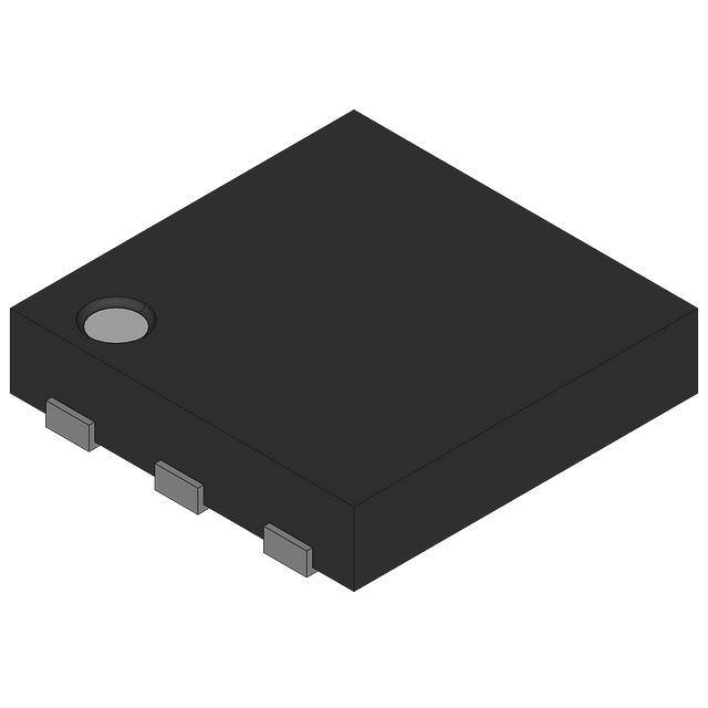
WDFN6 2x2, 0.65P
Typical Applications
• LED Display Backlight Control
D1
L1
22μH
VBAT
C1
1μF
C2
1μF
SW
SWIRE
VIN
PWM/
1-WIRE
GND
FCAP
FB
LV52204
C3
220nF
R1
10Ω
ORDERING INFORMATION
See detailed ordering and shipping information on page 16 of this data sheet.
Semiconductor Components Industries, LLC, 2014
May, 2014
51914NK/O1613NK 20130917-S00002/52213NK No.A2184-1/16
�LV52204MT
Specifications
Absolute Maximum Ratings at Ta = 25°C
Parameter
Symbol
Conditions
Ratings
Unit
Maximum supply voltage
VCC max
VCC
6.0
Maximum pin voltage1
V1 max
SW
40
V
V
Maximum pin voltage2
V2 max
Other pin
5.5
V
Allowable power dissipation
Pd max
Ta = 25°C *1
2.05
W
Operating temperature
Topr
-30 to +85
°C
Storage temperature
Tstg
-55 to +125
°C
*1 Mounted on a specified board: 70mm×50mm×1.2mm (4 layer glass epoxy)
Caution 1) Absolute maximum ratings represent the values which cannot be exceeded for any length of time.
Caution 2) Even when the device is used within the range of absolute maximum ratings, as a result of continuous usage under high temperature, high current,
high voltage, or drastic temperature change, the reliability of the IC may be degraded. Please contact us for the further details.
Stresses exceeding those listed in the Maximum Ratings table may damage the device. If any of these limits are exceeded, device functionality should not be assumed,
damage may occur and reliability may be affected.
Recommendation Operating Condition at Ta = 25°C
Parameter
Symbol
Conditions
Supply voltage range1
VCC op
VCC
PWM frequency
Fpwm
PWM MODE
PWM minimum duty
Fduty
Ratings
Unit
2.7 to 5.5
V
300 to 100k
Hz
10kHz, VIN ≥3.3V, –30°C to 85°C *2
2
%
20kHz, VIN ≥3.3V, –30°C to 85°C *2
4
%
30kHz, VIN ≥3.3V, –30°C to 85°C *2
6
%
*2 Guaranteed by design
Functional operation above the stresses listed in the Recommended Operating Ranges is not implied. Extended exposure to stresses beyond the Recommended
Operating Ranges limits may affect device reliability.
Electrical Characteristics Analog block at Ta = 25°C, VCC = 3.6V, unless otherwise specified
Parameter
Symbol
Conditions
Ratings
min
typ
SHUTDOWN
Unit
max
0
5
μA
1
mA
0.2
0.21
V
1
μA
39
V
Standby current dissipation
ICC1
DC/DC current dissipation
ICC2
VOUT = 30V, ILED = 20mA
FB voltage
Vfb
PWM duty 100%
FB pin leak current
Ifb
OVP voltage
Vovp
SWOUT ON resistance
Ron
IL = 100mA
700
NMOS switch current limit
ILIM
Vfb = 200mV
0.7
A
OSC frequency
Fosc
600
kHz
High level input voltage
VINH
SWIRE
1.5
VCC
Low level input voltage
VINL
SWIRE
0
0.4
Under voltage lockout
Vuvlo
VIN falling
SWIRE output voltage
Vack
Rpullup = 15kΩ
SW
0.19
37
38
mΩ
2.2
V
V
V
0.4
V
for Acknowledge
Product parametric performance is indicated in the Electrical Characteristics for the listed test conditions, unless otherwise noted. Product performance may not be
indicated by the Electrical Characteristics if operated under different conditions.
No.A2184-2/16
�LV52204MT
Recommended SWIRE Timing at Ta = 25°C, VCC = 3.6V, unless otherwise specified
Parameter
Symbol
SWIRE setup time1
Ton1
Ratings
Conditions
min
PWM duty more than 2%,
typ
Unit
max
2
μs
20
μs
VIN ≥3.3V, –30°C to 85°C *3
from shutdown
SWIRE setup time2
Ton2
from shutdown
SWIRE mode selectable time
Tsel
1
SWIRE delay time to start
Tw0
100
2.2
ms
μs
Tw1
260
μs
SWIRE low time to shutdown
Toff
8.9
ms
SWIRE start time for digital
Tstart
2
μs
Tend
2
digital mode detection
SWIRE low time to switch to
digital mode
mode programming
SWIRE end time for digital
360
μs
mode programming
SWIRE High time of bit 0
Th0
Bit detection = 0
2
180
μs
SWIRE Low time of bit 0
Tl0
Bit detection = 0
Th0 × 2
360
μs
μs
SWIRE High time of bit 1
Th1
Bit detection = 1
Tl1 × 2
360
SWIRE Low time of bit1
Tl1
Bit detection = 1
2
180
DCDC startup delay
Tdel
Delay time of Acknowledge
Tackd
Duration of Acknowledge
Tack
2
μs
ms
2
μs
512
μs
*3 Guaranteed by design
Block Diagram
VBAT
4
VCC
6
UVLO
TSD
PWM/
1-Wire
SWIRE
FCAP
SW
OCP
OVP
600kHz PWM
Controler
1
FB
5
VREF
CONTROL
2
VREF
3
GND
No.A2184-3/16
�LV52204MT
Pin Connections
6 VIN
FB 1
5 SWIRE/PWM
FCAP 2
GND 3
4 SW
Top view
Pin Function
PIN #
Pin Name
Description
1
FB
Feedback pin.
2
FCAP
Filtering capacitor terminal for PWM mode.
3
GND
Ground
4
SW
Switch pin. Drain of the internal power FET.
5
SWIRE
1-wire dimming control and PWM dimming input (active High).
6
VCC
Supply voltage.
Expose-pad
Connect to GND on PCB.
Allowable power dissipation, Pd max -- W
3.0
Pd max -- Ta
Mounted on a specified board: 70×50×1.2mm 3
(4 layer glass epoxy)
2.05
2.0
1.0
0.82
0
--30
0
30
60
90
120
Ambient temperature, Ta -- °C
No.A2184-4/16
�LV52204MT
LED Current Setting
LED current is set by an external resistor connected between the FB pin and ground.
ILED = VFB/RFB.
The VFB can be controled by two dimming modes, PWM Mode or Digital Mode.In PWM mode, PWM input is
converted into a near DC current by the internal resistor R that was equivalent to 60kΩ (±10%) and the external
capacitor CFCAP as a low pass filter with a cut-off frequency fc = 1/2πRFCAP. The VFB can be adjusted by altering
the duty cycle of the PWM signal (See Fig.1).
VFB = 200 (mV) × PWM Duty (%)
200
200
180
180
160
160
140
140
120
120
VFB (mV)
VFB (mV)
On the other hand, VFB can be selected one from among 32steps in Digital Mode (See Fig.2).
100
80
100
80
60
60
40
40
20
20
0
0
10
20
30
40
50
60
70
80
90
100
0
0
2
4
6
8
10 12 14 16 18 20 22 24 26 28 30 32
PWM Duty (%)
Data
Fig1. VFB vs. PWM Duty (PWM mode)
Fig2. VFB vs. Data Register Value (Digital mode)
Dimming Mode Selection
Dimming Mode is selected by a specific pattern of the SWIRE within Tsel (1ms) from the startup of the device every
time. In order to startup the device, the SWIRE must keep high for longer than Ton.
PWM Mode
The dimming mode is set to PWM mode when it is not recognized as a digital mode within Tsel. To enter Digital Mode,
the SWIRE is required keeping in low state for Tw1 (See Fig.4). If the PWM frequency is used faster than 6.6kHz, the
dimming mode is set to PWM mode only. But slower than 6.6kHz, it is necessary to avoid entering the digital mode
condition, such as SWIRE keeps high for longer than Tsel. PWM is enabled after Tdel from Tsel.
Ton
Tsel
Tdel
Toff
Shutdown
SWIRE
(PWM Freq > 6.6kHz)
PWM Enable
Tsel
Tdel
Toff
Shutdown
SWIRE
(PWM Freq < 6.6kHz)
PWM Enable
Fig3. SWIRE Timing Diagram in PWM mode
No.A2184-5/16
�LV52204MT
Digital Mode
To enter Digital Mode, SWIRE should be taken high for more than Tw0 (100μs) from the first rising edge and keep low
state for Tw1(260μs) before Tsel(1ms).
Tdel
Tsel
Tw1
SWIRE
Toff
Shutdown
Shutdown
Device Address & data
Tw0
Device Address & data
Digital Mode
Fig4. SWIRE Timing Diagram in Digital mode
It is required sending the device address byte and the data byte to select VFB. The bit detection is determined by the
ratio of Th and Tl (See Fig6). The start condition for the bit transmission required SWIRE high for at least Tstart. The
end condition is required SWIRE low for at least Tend.When data is not being transferred, SWIRE is set in the “H” state.
These registers are initialized with POR (Power On Reset).
In the LV52204MT, the device address (DA7 to DA0) is specified as “01110010”. D7 is setting for the acknowledge
response. If the device address and the data byte are transferred on D7 = 1, the ACK signal is sent from the receive side
to the send side. The acknowledge signal is issued when SWIRE on the send side is released and SWIRE on the receive
side is set to low state. D6 and D5 need to send 0. D4 to D0 allow to changing the FB voltage.
Register
BIT
Description
DA7
7
0
DA6
6
1
DA5
5
1
Device
DA4
4
1
Address
DA3
3
0
DA2
2
0
DA1
1
1
DA0
0
0
Table1. Device Address Description
Register
Data
BIT
Description
0 = Acknowledge disabled
D7
7
D6
6
D5
5
0
D4
4
Data bit 4
D3
3
Data bit 3
D2
2
Data bit 2
D1
1
Data bit 1
D0
0
Data bit 0
1 = Acknowledge enabled
0
Table2. Data Description
S
0
1
1
1
0
0
1
0
E
Device Address
S
0
1
1
1
0
0
S
0
0
FB Voltage Control
E
0
FB Voltage Control
E
ACK:Disable
1
0
E
S
Device Address
S
0
Start Condition
1
0
A
ACK:Enable
E
End Condition
A
Acknowledge
Fig5. Example of writing data
No.A2184-6/16
�LV52204MT
Tstart
Tstart
DA7
DA0
D7
D0
Tend
TI0 > Th0 * 2
Tend
Device Address
Data
(DA7 to DA0)
(D7 to D0)
Acknowledge : Disable (D7 = D0)
Tstart
TI0 Th0
Low state (Bit=0)
Tstart
Tack
TI1 > Th1 * 2
A
C
K
DA7
DA0
D7
TI1 Th1
High state (Bit=1)
D0
Tend
Tack
Device Address
Data
(DA7 to DA0)
(D7 to D0)
Acknowledge : Enable (D7 = 1)
Fig6.Bit detection Diagram
D7
D6
D5
D4
D3
D2
D1
D0
FB voltage (mV)
0
1/0
0
0
0
0
0
0
0
0
1
1/0
0
0
0
0
0
0
1
5
2
1/0
0
0
0
0
0
1
0
8
3
1/0
0
0
0
0
0
1
1
11
4
1/0
0
0
0
0
1
0
0
14
5
1/0
0
0
0
0
1
0
1
17
6
1/0
0
0
0
0
1
1
0
20
7
1/0
0
0
0
0
1
1
1
23
8
1/0
0
0
0
1
0
0
0
26
9
1/0
0
0
0
1
0
0
1
29
10
1/0
0
0
0
1
0
1
0
32
11
1/0
0
0
0
1
0
1
1
35
12
1/0
0
0
0
1
1
0
0
38
13
1/0
0
0
0
1
1
0
1
44
14
1/0
0
0
0
1
1
1
0
50
15
1/0
0
0
0
1
1
1
1
56
16
1/0
0
0
1
0
0
0
0
62
17
1/0
0
0
1
0
0
0
1
68
18
1/0
0
0
1
0
0
1
0
74
19
1/0
0
0
1
0
0
1
1
80
20
1/0
0
0
1
0
1
0
0
86
21
1/0
0
0
1
0
1
0
1
92
22
1/0
0
0
1
0
1
1
0
98
23
1/0
0
0
1
0
1
1
1
104
24
1/0
0
0
1
1
0
0
0
116
25
1/0
0
0
1
1
0
0
1
128
26
1/0
0
0
1
1
0
1
0
140
27
1/0
0
0
1
1
0
1
1
152
28
1/0
0
0
1
1
1
0
0
164
29
1/0
0
0
1
1
1
0
1
176
30
1/0
0
0
1
1
1
1
0
188
31
1/0
0
0
1
1
1
1
1
*200
(*Default)
Table3. Data Register vs. FB Voltage
No.A2184-7/16
�LV52204MT
Start up and Shutdown
The device becomes enabled when SWIRE is initially taken high.The dimming mode is determined within Tsel and the
boost converter start up after Tdel. To place the device into shutdown mode, the SWIRE must be held low for Toff.
PWM MODE
VIN
Tsel
Tdel
Toff
SWIRE
200m * duty
FB
Shutdown delay
FCAP
DCDC_EN
(internal signal)
Digital MODE
VIN
Tdel
Tsel
Toff
Tw1
SWIRE
Device Address & data
Tw0
Device Address & data
Programed value
Shutdown delay
FB
FCAP
DCDC_EN
(internal signal)
Fig7.Start up and shutdown diagram
No.A2184-8/16
�LV52204MT
Open LED Protection
If SW terminal voltage exceeds a threshold Vovp (38V typ) for 8 cycles, boost converter enters shutdown mode. In
order to restart the IC, SWIRE signal is required again.
Over Current Protection
Current limit value for built-in power MOS is around 0.7A. The power MOS is turned off for each switching cycle when
peak current through it exceeds the limit value.
Under Voltage Lock Out (UVLO)
UVLO operation works when VIN terminal voltage is below 2.2V.
Thermal Shutdown
When chip temperature is too high, boost converter is stopped.
Application Circuit Diagram
10LEDs
D1
L1
22μH
VBAT
C1
1μF
C2
1μF
5
4
FCAP SWIRE
GND
2
3
SW
6
VIN
FB
1
PWM/
1-Wire
C3
220nF
R1
10Ω
L1: VLS3012T-220M49 (TDK), VLF504015MT-220M (TDK)
D1: MBR0540T1 (ON semi), NSR05F40 (ONsemi)
C2: GRM21BR71H105K (Murata), C1608X5R1H105K (TDK)
No.A2184-9/16
�LV52204MT
6LEDs
D1
L1
10μH
VBAT
C1
1μF
C2
1μF
5
4
FCAP SWIRE
GND
2
3
SW
6
VIN
FB
1
PWM/
1-WIRE
C3
220nF
R1
10Ω
L1: VLS3012T-100M72 (TDK), VLF302512M-100M (TDK)
D1: MBR0540T1 (ON semi), NSR05F40 (ONsemi)
C2: GRM21BR71H105K (Murata), C1608X5R1H105K (TDK)
No.A2184-10/16
�LV52204MT
Typical Characteristics (VIN = 3.6V, L = 22μH, T = 25°C, unless otherwise specified)
Efficiency -- Output current
100
80
4.2V
6LED
8LED
70
60
50
40
10LED
90
10LED
Efficency -- %
Efficency -- %
90
Efficiency -- Output current
100
VIN=3.6V
80
3.6V
70
60
50
0
5
10
15
40
20
5
0
10
LED current -- mA
FB voltage -- mV
FB voltage -- mV
Mode=PWM
150
100
100
50
50
0
2
4
6
8
0
10 12 14 16 18 20 22 24 26 28 30 32
0
10
20
30
40
Data register
50
60
70
80
90
100
PWM duty -- %
FB voltage -- Temperature
200
180
160
160
140
140
FB voltage -- mV
180
120
DATA=16
100
FB voltage -- Temperature
200
DATA=31
80
60
Duty=100%
120
Duty=50%
100
80
60
40
40
DATA=06
20
0
--30
--15
0
Duty=10%
20
Mode=Digital
Mode=PWM
15
30
45
60
75
0
--30
90
Temperature -- °C
--15
0
15
30
45
60
75
90
Temperature -- °C
VIN current -- VIN
1000
20
LED current -- PWM frequency
800
75%
LED current -- mA
15
ICC -- µA
20
FB voltage -- PWM duty
200
Mode=Digital
150
FB voltage -- mV
15
LED current -- mA
FB voltage -- DATA register
200
0
3.0V
600
400
50%
10
25%
5
200
0
2
3
4
VIN -- V
5
6
0
0.1
1
10
100
PWM frequency -- kHz
No.A2184-11/16
�LV52204MT
PACKAGE DIMENSIONS
WDFN6 2x2, 0.65P
CASE 511BR-01
ISSUE O
D
A
B
EXPOSED Cu
NOTES:
1. DIMENSIONING AND TOLERANCING PER
ASME Y14.5M, 1994.
2. CONTROLLING DIMENSION: MILLIMETERS.
3. DIMENSION b APPLIES TO PLATED
TERMINAL AND IS MEASURED BETWEEN
0.15 AND 0.25 mm FROM THE TERMINAL TIP.
4. COPLANARITY APPLIES TO THE EXPOSED
PAD AS WELL AS THE TERMINALS.
MOLD CMPD
DETAIL B
ALTERNATE
CONSTRUCTIONS
PIN ONE
REFERENCE
E
0.10 C
0.10 C
DIM
A
A1
A3
b
D
D2
E
E2
e
L
L1
L
L
L1
TOP VIEW
DETAIL A
0.05 C
ALTERNATE
CONSTRUCTIONS
A3
DETAIL B
MILLIMETERS
MIN
MAX
0.70
0.80
0.00
0.05
0.20 REF
0.25
0.35
2.00 BSC
1.50
1.70
2.00 BSC
0.90
1.10
0.65 BSC
0.40
0.20
--0.15
A
6X
0.05 C
A1
NOTE 4
C
SIDE VIEW
GENERIC
MARKING DIAGRAM*
SEATING
PLANE
1
XX M
D2
DETAIL A
XX = Specific Device Code
M = Date Code
L
1
3
*This information is generic. Please refer to
device data sheet for actual part marking.
Pb−Free indicator, G or microdot ,
may or may not be present.
E2
4
6
6X
RECOMMENDED
MOUNTING FOOTPRINT
b
e
BOTTOM VIEW
0.10 M
C A B
0.05 M
C
1.72
NOTE 3
6X
0.45
1.12
PACKAGE
OUTLINE
6X
0.40
2.30
1
0.65
PITCH
DIMENSIONS: MILLIMETERS
LV52204MT is as follows.
MARKING DIAGRAM
W4M
W4 = Device Code
M = Date Code
= Pb-Free Package
PS No.A2184-12/16
�LV52204MT
PS No.A2184-13/16
�LV52204MT
PS No.A2184-14/16
�LV52204MT
PS No.A2184-15/16
�LV52204MT
ORDERING INFORMATION
Device
LV52204MTTBG
Package
WDFN6 (2x2)
(Pb-Free)
Shipping (Qty / Packing)
3000 / Tape & Reel
ON Semiconductor and the ON logo are registered trademarks of Semiconductor Components Industries, LLC (SCILLC). SCILLC owns the rights to a number
of patents, trademarks, copyrights, trade secrets, and other intellectual property. A listing of SCILLC’s product/patent coverage may be accessed at
www.onsemi.com/site/pdf/Patent-Marking.pdf. SCILLC reserves the right to make changes without further notice to any products herein. SCILLC makes no
warranty, representation or guarantee regarding the suitability of its products for any particular purpose, nor does SCILLC assume any liability arising out of the
application or use of any product or circuit, and specifically disclaims any and all liability, including without limitation special, consequential or incidental
damages. “Typical” parameters which may be provided in SCILLC data sheets and/or specifications can and do vary in different applications and actual
performance may vary over time. All operating parameters, including “Typicals” must be validated for each customer application by customer’s technical
experts. SCILLC does not convey any license under its patent rights nor the rights of others. SCILLC products are not designed, intended, or authorized for use
as components in systems intended for surgical implant into the body, or other applications intended to support or sustain life, or for any other application in
which the failure of the SCILLC product could create a situation where personal injury or death may occur. Should Buyer purchase or use SCILLC products for
any such unintended or unauthorized application, Buyer shall indemnify and hold SCILLC and its officers, employees, subsidiaries, affiliates, and distributors
harmless against all claims, costs, damages, and expenses, and reasonable attorney fees arising out of, directly or indirectly, any claim of personal injury or
death associated with such unintended or unauthorized use, even if such claim alleges that SCILLC was negligent regarding the design or manufacture of the
part. SCILLC is an Equal Opportunity/Affirmative Action Employer. This literature is subject to all applicable copyright laws and is not for resale in any manner.
PS No.A2184-16/16
�