Ordering number : ENA0438F
LV8044LP
Bi-CMOS IC
6-channel Motor Driver IC
for Digital Still Camera
http://onsemi.com
Overview
The LV8044LP is a 6-channel motor driver IC for digital still camera.
Functions
Two microstep drive H-bridge driver channels.
Two microstep drive/PWM saturated drive switchable H-bridge driver channels.
Two constant-current drive H-bridge driver channels.
Drive mode switchable between 2-phase, 1-2 phase full torque, 1-2 phase, and 4W1-2 phase (channels 1, 2, 3, and 4).
Microstep drive step advance controlled by a single step signal input (channels 1, 2, 3, and 4).
Ability to set the hold current to one of four levels (channels 1, 2, 3, and 4).
Ability to set the constant-current reference voltage to one of 16 levels from the serial data (channels 5 and 6).
Eight-bit 3-wire serial control.
Three on-chip photosensor driver circuits.
Specifications
Maximum Ratings at Ta = 25C
Parameter
Symbol
Conditions
Ratings
Unit
Power supply voltage 1
VM max
6.0
V
Power supply voltage 2
VCC max
6.0
V
Output peak current
IO peak
Each CH tw 10ms, duty 20%
600
mA
Output continuous current
IO max
Each CH
400
mA
Allowable power dissipation 2
Pd max
With substrate *
1.4
W
-20 to +85
C
Operating temperature
Topg
Storage temperature
Tstg
C
-55 to +150
*: With 40mm × 50mm × 0.8mm glass epoxy substrate (four-layer substrate).
Caution 1) Absolute maximum ratings represent the value which cannot be exceeded for any length of time.
Caution 2) Even when the device is used within the range of absolute maximum ratings, as a result of continuous usage under high temperature, high current,
high voltage, or drastic temperature change, the reliability of the IC may be degraded. Please contact us for the further details.
Stresses exceeding Maximum Ratings may damage the device. Maximum Ratings are stress ratings only. Functional operation above the Recommended Operating
Conditions is not implied. Extended exposure to stresses above the Recommended Operating Conditions may affect device reliability.
ORDERING INFORMATION
See detailed ordering and shipping information on page 26 of this data sheet.
Semiconductor Components Industries, LLC, 2013
December, 2013
D2013HK 20130730-S00003/O1911SY/O2710SY/50710SY/
12408MS/32807MSPC/71906MSOT No.A0438-1/26
�LV8044LP
Recommended Operating Conditions at Ta = 25C
Parameter
Symbol
Conditions
Ratings
Unit
Power supply voltage range 1
VM
2.7 to 5.5
V
Power supply voltage range 2
VCC
2.7 to 5.5
V
Logic input voltage range
VIN
0 to VCC +0.3
V
STEP frequency
FSTEP
STEP1, STEP2
to 64
KHz
PWM frequency
FPWM
STEP3, STEP4
to 100
KHz
Electrical Characteristics at Ta 25C, VM = 5V, VCC = 3.3V
Parameter
Standby supply current
Symbol
ISTN
Motor supply current
IM
Logic supply current
ICC
Conditions
Ratings
min
typ
Unit
max
1.0
A
50
100
A
2
3
4
mA
2.1
2.35
2.6
V
100
150
200
mV
150
180
200
ST = “L”
ST = “H”, PWM3 = PWM4 = “H”,
IN51 = IN61 = “H”, no load
ST = “H”, PWM3 = PWM4 = “H”,
IN51 = IN61 = “H”, no load
VCC low-voltage cut voltage
VthVCC
Low-voltage hysteresis voltage
VthHIS
Thermal shutdown temperature
TSD
Design guarantee
TSD
Design guarantee
Thermal hysteresis width
C
C
40
Microstep Driver (channels 1, 2, 3, and 4)
Output on resistance
Output leak current
IO = 400mA, Upper ON resistance
0.7
0.8
Rond
IO = 400mA, Lower ON resistance
0.5
0.6
1.0
A
IOleak1
Diode forward voltage 1
VD1
ID = -400mA
Logic pin input current
IinL
VIN = 0V (ST, STEP1, STEP2)
IinH
VIN = 3.3V (ST, STEP1, STEP2)
20
2.5
Logic input “H” level voltage
Vinh
ST, STEP1, STEP2
Logic input “L” level voltage
Vinl
ST, STEP1, STEP2
Current
4W1-2 phase
Ronu
Vstep16
selection
Step 16
0.9
33
1.2
V
1.0
A
50
A
1.0
V
V
0.185
0.200
0.215
V
(Initial level: the channel 1 comparator level)
reference
Vstep15
Step 15 (Initial+1)
0.185
0.200
0.215
V
voltage level
Vstep14
Step 14 (Initial+2)
0.185
0.200
0.215
V
Vstep13
Step 13 (Initial+3)
0.176
0.193
0.206
V
Vstep12
Step 12 (Initial+4)
0.170
0.186
0.200
V
Vstep11
Step 11 (Initial+5)
0.162
0.178
0.192
V
Vstep10
Step 10 (Initial+6)
0.154
0.171
0.184
V
Vstep9
Step 9 (Initial+7)
0.146
0.163
0.176
V
Vstep8
Step 8 (Initial+8)
0.129
0.148
0.159
V
Vstep7
Step 7 (Initial+9)
0.113
0.131
0.143
V
Vstep6
Step 6 (Initial+10)
0.097
0.115
0.127
V
Vstep5
Step 5 (Initial+11)
0.079
0.097
0.109
V
Vstep4
Step 4 (Initial+12)
0.062
0.079
0.092
V
Vstep3
Step 3 (Initial+13)
0.044
0.06
0.074
V
Vstep2
Step 2 (Initial+14)
0.024
0.04
0.054
V
Vstep1
Step 1 (Initial+15)
0.006
0.02
0.036
V
Step 16
0.185
0.200
0.215
V
Step 8 (Initial+1)
0.129
0.148
0.159
V
Step 16
0.185
0.200
0.215
V
1-2 phase
Vstep16
(Initial level: the channel 1 comparator level)
Vstep8
1-2 phase
Vstep16
(Full torque)
2 phase
(Initial level: the channel 1 comparator level)
Vstep8
Step 8 (Initial+1)
0.185
0.200
0.215
V
Vstep8
Step 8
0.185
0.200
0.215
V
Continued on next page.
No.A0438-2/26
�LV8044LP
Continued from preceding page.
Parameter
Chopping frequency
Current setting reference voltage
Symbol
Conditions
Ratings
min
typ
Unit
max
fchop1
104
130
156
KHz
fchop2
52
65
78
KHz
fchop3
160
200
240
KHz
fchop4
80
100
120
KHz
VSEN00
(D5, D6) = (0, 0)
0.185
0.200
0.215
V
VSEN01
(D5, D6) = (0, 1)
0.119
0.134
0.149
V
VSEN10
(D5, D6) = (1, 0)
0.085
0.100
0.115
V
VSEN11
(D5, D6) = (1, 1)
0.051
0.066
0.081
V
Constant-Current Drive (channels 5 and 6)
Output on resistance
Output leak current
Ronu
IO = 400mA, Upper ON resistance
0.7
0.8
Rond
IO = 400mA, Lower ON resistance
0.5
0.6
1.0
μA
IOleak
Diode forward voltage 1
VD1
ID = -400mA
Logic pin input current
IinL
VIN = 0V, (IN51, IN52, IN61, IN62)
IinH
VIN = 3.3V, (IN51, IN52, IN61, IN62)
20
2.5
Logic input “H” level voltage
Vinh
IN51, IN52, IN61, IN62
Logic input “L” level voltage
Vinl
IN51, IN52, IN61, IN62
Output constant current
IOUT
Rload = 3,RF = 0.5,
0.9
33
1.2
V
1.0
A
50
A
1.0
V
mA
V
380
400
420
Internal standard = 0.2V
Current setting reference voltage
Vref0
(D4, D5, D6, D7) = (0, 0, 0, 0)
0.285
0.30
0.315
V
Vref1
(D4, D5, D6, D7) = (1, 0, 0, 0)
0.19
0.20
0.21
V
Vref2
(D4, D5, D6, D7) = (0, 1, 0, 0)
0.18
0.190
0.2
V
Vref3
(D4, D5, D6, D7) = (1, 1, 0, 0)
0.171
0.180
0.189
V
Vref4
(D4, D5, D6, D7) = (0, 0, 1, 0)
0.161
0.170
0.179
V
Vref5
(D4, D5, D6, D7) = (1, 0, 1, 0)
0.156
0.165
0.173
V
Vref6
(D4, D5, D6, D7) = (0, 1, 1, 0)
0.152
0.160
0.168
V
Vref7
(D4, D5, D6, D7) = (1, 1, 1, 0)
0.147
0.155
0.163
V
Vref8
(D4, D5, D6, D7) = (0, 0, 0, 1)
0.143
0.150
0.158
V
Vref9
(D4, D5, D6, D7) = (1, 0, 0, 1)
0.137
0.145
0.152
V
VrefA
(D4, D5, D6, D7) = (0, 1, 0, 1)
0.133
0.140
0.147
V
VrefB
(D4, D5, D6, D7) = (1, 1, 0, 1)
0.128
0.135
0.142
V
VrefC
(D4, D5, D6, D7) = (0, 0, 1, 1)
0.123
0.130
0.137
V
VrefD
(D4, D5, D6, D7) = (1, 0, 1, 1)
0.114
0.120
0.126
V
VrefE
(D4, D5, D6, D7) = (0, 1, 1, 1)
0.104
0.110
0.116
V
VrefF
(D4, D5, D6, D7) = (1, 1, 1, 1)
0.095
0.100
0.105
V
Vsat
IO = -20mA
0.09
0.12
V
1.0
A
50
A
Photo-sensor Drive Circuit
Output saturation voltage
Serial Data Transfer Pin
Logic pin input current
IinL
VIN = 0V (SCLK, SDATA, STB)
IinH
VIN = 3.3V (SCLK, SDATA, STB)
20
Vinh
SCLK, SDATA, STB
2.5
Logic input “L” level voltage
Vinl
SCLK, SDATA, STB
Minimum SLCK “H” pulse width
Tckh
0.125
s
Minimum SLCK “L” pulse width
Tckl
0.125
s
Tsup1
0.125
s
Tsup2
0.125
s
Tstbw
0.125
s
Tds
0.125
s
Data hold time
Tdh
0.125
Maximum SCLK frequency
Fclk
Logic input “H” level voltage
Minimum setup time
33
V
1.0
V
(STB SCLK rising edge)
Minimum setup time
(SCLK rising edge STB)
Minimum STB pulse width
Data setup time
s
4
MHz
No.A0438-3/26
�LV8044LP
Serial Input Switching Characteristics Timing Chart
Fclk
Tsup1
Tckh
Tckl
SCLK
Tds Tdh
D0
SDATA
D1
D2
D6
D7
Tsup2
STB
Tstbw
Package Dimensions
unit : mm (typ)
[LV8044LP]
TOP VIEW
BOTTOM VIEW
SIDE VIEW
5.0
40
(0.7)
0.4
5.0
0.35
0.35
SIDE VIEW
0.85 MAX
0.0 NOM
2 1
(0.7)
0.2
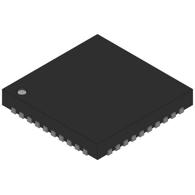
SANYO : VQLP40(5.0X5.0)
Pd max -- Ta
[LV8044LP]
Specified substrate: 40×50×0.8mm3
glass epoxy four-layer board.
Allowable power dissipation, Pd max -- W
1.6
1.4
1.2
0.8
0.73
0.4
0
-20
0
20
40
60
80 85
100
Ambient temperature, Ta -- °C
No.A0438-4/26
�LV8044LP
28
27
26
25
24
23
22
RF6
OUT6A
OUT4B
RF4
OUT4A
OUT3B
RF3
21
OUT3A
29
OUT6B
31 IN62
30
PGND2
Pin Assignment
PWM3/
20
STEP2
32 IN61
PWM4 19
33 VM6
VM34 18
VCC 17
34 SGND
LV8044LP
LV8044LQ
35 PI1
STB 16
SDATA 15
36 PI2
TOP VIEW
37 PI3/MO
SCLK 14
OUT2B
RF2
OUT2A
OUT1B
RF1
OUT1A
40 IN51
OUT5A
VM12 12
RF5
39 IN52
OUT5B
STEP1 13
PGND1
38 VM5
1
2
3
4
5
6
7
8
9
10
ST 11
The pin assignment of LV8044LP and LV8044LQ is the same.
No.A0438-5/26
�SGND
VCC
PGND1
RF1
Current selection
LVS
TSD
VM12
STEP1
OUT2B
Oscillator
Current selection
(4W1-2/1-2/
1-2Full/2)
OUT2A
Output control logic
OUT1B
(4W1-2/1-2/
1-2Full/2)
OUT1A
Monitor
selector
SCLK
SDATA
STB
(4W1-2/1-2/
1-2Full/2)
ST
VM34
OUT4A
STEP2
/PWM3
PWM4
(4W1-2/1-2/
1-2Full/2)
OUT4B
Current selection
Output control logic
OUT3B
Current selection
RF3 OUT3A
Serial-to-parallel
converter (8 bits)
RF2
OUT5B
Reference
voltage
circuit (0.3 V)
MO/PI3
RF5
Reference voltage
selection circuit
(0.1 to 0.3 V in 16 steps)
Output control
logic
VM5 OUT5A
IN51 IN52 IN61 IN62
RF4
RF6
PI1 V
PI2
CC
OUT6B
Output control
logic
VM6 OUT6A
PGND2
LV8044LP
Block Diagram
No.A0438-6/26
�LV8044LP
Pin Function
Pin No.
Pin name
13
STEP1
20
PWM3/STEP2
Function
Equivalent circuit
Channels 1/2 - STEP signal input
3ch PWM signal input
/ Channels 3/4 - STEP signal input
19
PWM4
40
IN51
39
IN52
4ch PWM signal input
Channel 5 - Logic input 1
32
IN61
31
IN62
Channel 6- Logic input 1
14
SCLK
15
SDATA
16
STB
11
ST
10
OUT1A
1ch
7
OUT2A
2ch
21
OUT3A
3ch
24
OUT4A
4ch
4
OUT5A
5ch
27
OUT6A
6ch
8
OUT1B
1ch
Serial data transfer clock input
Serial data input
Serial data latch pulse input
Chip enable
5
OUT2B
2ch
23
OUT3B
3ch
26
OUT4B
4ch
2
OUT5B
5ch
29
OUT6B
6ch
9
RF1
1ch
6
RF2
2ch
22
RF3
3ch
25
RF4
4ch
5ch
OUTA output
OUTB output
Current sensing resistor connection
3
RF5
28
RF6
12
VM12
Channels 1/2 - Motor power supply
18
VM34
Channels 3/4 - Motor power supply
38
VM5
Channels 5 - Motor power supply
33
VM6
Channels 6 - Motor power supply
35
PI1
Photosensor drive output
36
PI2
6ch
Continued on next page.
No.A0438-7/26
�LV8044LP
Continued from preceding page.
Pin No.
Pin name
37
PI3/MO
Function
Equivalent circuit
Photosensor drive output 3/position detection monitor
17
VCC
1
PGND1
Logic system power supply
30
PGND2
Channels 3/4/6 - Power system ground
34
SGND
Signal system ground
Channels 1/2/5 - Power system ground
Serial Data Input Specifications
1. Serial Data Input Setup
First set STB low and then input the SDATA and SCLK signals. The SCLK signal is not accepted when STB is high.
SDATA inputs the data in the order D0, D1, ... D6, D7.
Data is transferred on the rising edge of SCLK and after all data has been transferred, all the data is latched on the rising
edge of STB.
2. Timing with which the Serial Data Settings are Reflected in the Output
STP timing mode (applies to microstep driver settings)
Type 1: The hold, reset, and enable settings, as well as the reference voltage setting are reflected at the same time as
the STB signal data latch operation.
Type 2: The forward/reverse (FR) and the excitation setting mode (MS) setting that are set at STP setup are reflected
in the output at the next clock rising edge after data latch.
STB timing (applies to settings other than the above)
Type 1: The PWM driver, constant-current driver, PI, and other settings are reflected at the same time as the STB signal
data latch operation.
No.A0438-8/26
�LV8044LP
Serial Data Truth Table
Serial Logic Table (1)
Input
Setting mode
Description
D0 D1 D2 D3 D4 D5 D6 D7
0
1
0
0
0
0
0
0
*
*
*
1
0
*
*
*
*
*
*
1ch 2ch 3ch 4ch 5ch 6ch
Channels 1 and 2
excitation
1
1
*
*
*
4W1-2 phase
*
*
0
0
*
100% (0.2V)
*
*
1
0
*
*
*
0
1
*
*
*
1
1
*
*
*
*
*
0
*
*
*
*
1
0
*
*
*
*
1/2ch energization
CW (Forward)
1
*
*
*
*
direction
CCW (Reverse)
*
0
*
*
*
*
1
*
*
*
*
*
0
*
*
*
*
1
*
*
*
*
0
*
*
*
1
*
*
*
*
*
0
*
*
*
*
1
timing
PI
STEP1 STEP2
STB
1-2 phase (full torque)
1
*
Remarks
Serial data reflection
2 phase
0
*
Set channel
mode selection
Channels 1 and 2
current reference
voltage selection
1-2 phase
67% (0.134V)
50% (0.1V)
33% (0.066V)
(Dummy data)
Cancel
1/2ch step hold
Hold
Reset
1/2ch counter reset
Cancel
Output OFF
1/2ch output enable
Output ON
(Dummy data)
No.A0438-9/26
�LV8044LP
Serial Logic Table (2)
Input
Setting mode
Description
D0 D1 D2 D3 D4 D5 D6 D7
0
1
0
0
0
*
*
*
1
0
*
*
*
0
1
*
*
*
1
1
*
*
*
*
*
0
0
*
*
*
1
0
*
*
*
0
1
*
*
*
1
1
*
*
*
*
*
0
*
*
*
*
1
Remarks
Set channel
1ch 2ch 3ch 4ch 5ch 6ch
Serial data reflection
PI
timing
STEP1 STEP2
STB
2 phase
3/4ch
excitation
mode selection
1-2 phase (full torque)
1-2 phase
4W1-2 phase
100% (0.2V)
3/4ch
current reference
voltage selection
67% (0.134V)
50% (0.1V)
33% (0.066V)
3/4ch
PWM
Channels 3 and 4
Microstep
saturation/microstep
selection
0
0
*
*
*
1
0
*
*
*
0
1
*
*
*
1
1
*
*
*
*
*
0
0
*
*
*
1
0
*
*
1
1
0
*
OFF
3ch energization
direction
(Saturated mode)
OUT3A OUT3B
OUT3B OUT3A
Brake
OFF
4ch energization
direction
OUT4B OUT4A
*
0
1
*
*
1
1
*
*
*
*
*
0
3/4ch PWM DECAY
Brake
Standby mode
CW (Forward)
(Saturated mode)
OUT4A OUT4B
Brake
*
*
*
*
1
(Saturated mode)
0
*
*
*
*
1
*
*
*
*
3/4ch energization
direction
(Microstep mode)
CCW (Reverse)
*
0
*
*
*
3/4ch step hold
Cancel
*
1
*
*
*
(Microstep mode)
Hold
*
*
0
*
*
3/4ch counter reset
Reset
*
*
1
*
*
(Microstep mode)
Cancel
*
*
*
0
*
3/4ch output enable
Output OFF
*
*
*
1
*
(Microstep mode)
Output ON
*
*
*
*
0
*
*
*
*
1
(Dummy data)
No.A0438-10/26
�LV8044LP
Serial Logic Table (3)
Input
Setting mode
Description
Remarks
D0 D1 D2 D3 D4 D5 D6 D7
0
1
0
0
1
1
Serial data reflection
Set channel
PI
1ch 2ch 3ch 4ch 5ch 6ch
timing
STEP1 STEP2
STB
OFF
0
0
*
*
*
1
0
*
*
*
5ch energization
OUT5A OUT5B
direction
OUT5B OUT5A
0
1
*
*
*
1
1
*
*
*
Brake
*
*
0
0
*
OFF
*
*
1
0
*
6ch energization
OUT6A OUT6B
*
*
0
1
*
direction
OUT6B OUT6A
*
*
1
1
*
*
*
*
*
0
*
*
*
*
1
0
*
*
*
*
Reference setting
5ch setting
channel selection
6ch setting
*1
*2
Brake
(Dummy data)
1
*
*
*
*
*
0
0
0
0
0.300V
*
1
0
0
0
0.200V
*
0
1
0
0
0.190V
*
1
1
0
0
0.180V
*
0
0
1
0
0.170V
*
1
0
1
0
0.165V
*
0
1
1
0
0.160V
*
1
1
1
0
Constant-current
0.155V
*
0
0
0
1
reference voltage
0.150V
*
1
0
0
1
0.145V
*
0
1
0
1
0.140V
*
1
1
0
1
0.135V
*
0
0
1
1
0.130V
*
1
0
1
1
0.120V
*
0
1
1
1
0.110V
*
1
1
1
1
0.100V
No.A0438-11/26
�LV8044LP
Serial Logic Table (4)
Input
Setting mode
Description
Remarks
D0 D1 D2 D3 D4 D5 D6 D7
0
1
1
1
1
1
0
*
*
*
*
1
*
*
*
*
*
0
*
*
*
*
1
*
*
*
*
*
0
*
*
*
*
1
*
*
*
*
*
0
*
*
*
*
1
*
*
*
*
*
0
*
*
*
*
1
0
*
*
*
*
1
*
*
*
*
*
0
*
*
*
*
1
*
*
*
*
*
0
*
*
*
*
1
*
*
*
*
*
0
0
*
*
*
1
0
*
*
*
0
1
*
*
*
1
1
Set channel
Serial data reflection
PI
1ch 2ch 3ch 4ch 5ch 6ch
timing
STEP1 STEP2
STB
OFF
Photo-sensor drive 1
Photo-sensor drive 2
Photo-sensor drive 3
(When PI3 output
selected)
ON
OFF
ON
OFF
ON
(Dummy data)
(Dummy data)
PI3/MO select
MO output channel
selection
(When MO output
selected)
MO output position
PI3 Output
MO output
1/2ch
3/4ch
*3
Initial position
1-2 phase
*4
130KHz
Chopping frequency
setting
65KHz
200KHz
100KHz
Notes
*1: This serial data is only accepted when the IN51/IN52 pulse inputs are in the Low/Low states, respectively. It is
ignored at all other times.
*2: This serial data is only accepted when the IN61/IN62 pulse inputs are in the Low/Low states, respectively. It is
ignored at all other times.
*3: When D4 = 1, MO is only output if microstep mode is selected for channels 3 and 4. In PWM mode, this output is held
fixed at the high level.
*4: The MO output can be specified to be the 1-2 phase position only in 4W1-2 phase excitation mode. In all other
excitation modes, the MO output position becomes the initial position regardless of the serial data values.
No.A0438-12/26
�LV8044LP
Channels 1 and 2 Driver Circuit (Microstep drive stepping mode driver)
STEP1 Pin Function
Input
ST
STEP1
Low
*
High
Operating mode
Standby mode
Excitation step feed
High
Excitation step hold
Excitation Mode Setting (D0 = 0, D1 = 0, D2 = 0)
D3
D4
Excitation mode
0
0
1
0
1
Initial position
1ch
2ch
2 phase excitation
100%
-100%
0
1-2 phase excitation (full torque)
100%
0%
1
1-2 phase excitation
100%
0%
1
4W1-2 phase excitation
100%
0%
The initial state at power on is the initial position for each excitation mode when the counter is reset.
Reference Voltage Setting Serial Data: (D0 = 0, D1 = 0, D2 = 0)
D5
D6
0
0
Current setting reference voltage (When microstep is 100%)
0.2V
1
0
0.134V
0
1
0.1V
1
1
0.066V
The output current setting reference voltage can be switched between four levels with the serial data.
This setting is useful for saving power in the motor powered hold state.
Calculating the Set Current
Since the reference voltage can be modified (0.2, 0.134, 0.1, and 0.66V) with the serial data, the output current can be
set with the reference voltage and the resistor RF connected between the RF pin and ground.
IOUT = ( × )/
Example: If the reference voltage is 0.2 V, the set current ratio is 100%, and the RF resistor value is 1, then the output
current will be that shown below.
IOUT = 0.2V 100%/1 = 200mA
No.A0438-13/26
�LV8044LP
Output Current Vector Locus (With one step normalized to 90 degrees)
Set Current Ratios in the Different Excitation Modes
STEP
4W1-2 phase (%)
1ch
1-2 phase (%)
2ch
1ch
0
0
100
1
10
100
2
20
100
3
30
96.5
4
39.5
93.0
5
48.5
89
6
57.5
85.5
7
65.5
81.5
8
74.0
74.0
9
81.5
65.5
10
85.5
57.5
11
89
48.5
12
93.0
39.5
13
96.5
30
14
100
20
15
100
10
16
100
0
1-2 phase full torque (%)
2ch
1ch
2ch
2 phase (%)
1ch
0
100
0
100
74.0
74.0
100
100
100
0
100
0
100
2ch
100
No.A0438-14/26
�LV8044LP
2 Phase Excitation (CW mode)
1-2 Phase Excitation full torque (CW mode)
1-2 Phase Excitation (CW mode)
No.A0438-15/26
�LV8044LP
4W1-2 Phase Excitation (CW mode)
No.A0438-16/26
�LV8044LP
Current Control Operation Specifications
Sine wave increasing direction
STEP
Set current
Coil current
Set current
fchop
Current
mode
CHARGE
SLOW
FAST
CHARGE
SLOW
FAST
Sine wave decreasing direction
STEP
Set current
Coil current
Set current
fchop
Current
mode
CHARGE
SLOW
FAST
CHARGE
FAST
CHARGE
SLOW
Each of the current modes operates with the follow sequence.
The IC enters charge mode when the chopping oscillation starts. (A period of charge mode is forcibly present in 1/8
of the period, regardless of which of the coil current (ICOIL) and the set current (IREF) is larger.)
In charge mode, the coil current (ICOIL) and the set current (IREF) are compared.
If an ICOIL < IREF state exists during the charge period:
The IC operates in charge mode until ICOIL IREF. After that, it switches to slow decay mode and then switches to
fast decay mode in the last 1/8 of the period.
If no ICOIL < IREF state exists during the charge period:
The IC switches to fast decay mode and the coil current is attenuated with the fast decay operation until the end of the
chopping period.
The above operation is repeated. Normally, in the sine wave increasing direction the IC operates in slow (+fast) decay
mode, and in the sine wave decreasing direction the IC operates in fast decay mode until the current is attenuated and
reaches the set value and the IC operates in slow decay mode.
No.A0438-17/26
�LV8044LP
Chopping Frequency Setting (D6 and D7 in the serial data)
This IC integrates an internal oscillator circuit and allows the chopping frequency used in constant-current control to be
switched with the serial data (111***, D6, D7) setting.
Data D6
Data D7
Chopping frequency
0
0
130KHz
1
0
65KHz
0
1
200KHz
1
1
100KHz
Monitor Output Setting (Serial data bits D3, D4, and D5)
The signal output from the PI3/MO pin can be switched with the serial data (111, D3, ****) setting.
Data D3
PI3/MO pin output
0
Photosensor drive output 3
1
Stepping position detection monitor output
It is also possible to select which of channels 1 and 2 or channels 3 and 4 are output from the monitor pin with the serial
data (111*, D4, D5, **) setting. The MO output position used to detect the driver excitation position in microstepping
drive mode can also be switched. The state MO = Low is output at the output position.
Data D4
Data D5
0
0
0
1
Channels 1 and 2
Channels 3 and 4 excitation
excitation mode
mode
MO output
2 phase excitation
Channels 1 and 2 monitor/initial position
Channels 1 and 2 monitor/initial position
0
0
1-2 phase excitation
0
1
(full torque)
0
0
1-2 phase excitation
Channels 1 and 2 monitor/initial position
0
1
4W1-2 phase excitation
Channels 1 and 2 monitor/initial position
0
0
0
1
1
0
1
1
1
0
1
1
1
0
1
1
1
0
1
1
1
0
1
1
Channels 1 and 2 monitor/1-2 phase position
2 phase excitation
Channels 3 and 4 monitor/initial position
1-2 phase excitation (full torque)
Channels 3 and 4 monitor/initial position
1-2 phase excitation
Channels 3 and 4 monitor/initial position
4W1-2 phase excitation
Channels 3 and 4 monitor/initial position
Channels 3 and 4 monitor/1-2 phase position
PWM drive mode
Output held fixed at the high level
No.A0438-18/26
�LV8044LP
Basic Set Current Step Switching (STEP pin) and Forward/Reverse Switching (D3 in the serial data)
Operations
The IC internal D/A converter advances by 1 bits on the rising edge of the input step pulse.
The CW/CCW mode can be switched with the serial data (100, D3, ****) setting. The operation progresses with the
position number decreasing in CW mode and increasing in CCW mode.
In CW mode, the channel 2 current phase is delayed by 90 degrees relative to the channel 1 current.
In CCW mode, the channel 2 current phase is advanced by 90 degrees relative to the channel 1 current.
No.A0438-19/26
�LV8044LP
Excitation Mode Switching During Operation (D3 and D4 in the serial data)
If the excitation mode is switched when power is applied to the motor, the operation follows the sequence shown below.
(CW mode)
Before excitation mode switching
Excitation mode
Position
Step position after excitation mode switching
4W1-2 phase
1-2 phase
2 phase full
2 phase
torque
4W1-2 phase
1-2 phase
2 phase full torque
2 phase
(16)
(8)
(8)’
(8)’
(15) to (9)
(8)
(8)’
(8)’
(8)’
(8)
0
0
(7) to (1)
(8)
(8)’
(8)’
0
-(8)
-(8)’
-(8)’
(8)’
(16)
(15)
(8)’
(8)
(7)
0
(8)’
0
-(1)
-(8)’
-(8)’
(16)
(15)
(8)
(8)’
(7)
0
(8)’
0
-(1)
-(8)
-(8)’
(8)’
(7)
0
(8)’
0
No.A0438-20/26
�LV8044LP
Output Enable Function (D6 in the serial data)
When the OE bit in the serial data, D6 (100, ***, D6, *), is set to 0, the output is turned off and set to the
high-impedance state at the rise of STB.
Since, however, the internal logic circuits operate in this state, the position number will be advanced if a step input is
applied. Therefore, when the OE bit (D6) is returned to 1, a level according to the position number advanced by the step
input will be output.
Counter Reset Function (D5 in the serial data)
When the reset bit in the serial data, D5 (100, **, D5, **), is set to 0, the output goes to the initial state at the rise of STB
and the MO output goes low.
Then, when the reset bit (D5) is next set to 1, the position number will advance at the next step input.
No.A0438-21/26
�LV8044LP
Step Hold Function (D4 in the serial data)
When the hold bit in the serial data, D4 (100, *, D4, ***), is set to 1, the external step state at that time is held without
change as the internal step state.
Since the (external) step state is low at the timing of the step hold operation (1) in the figure, the internal step state is
held at the low level, and since the (external) step state is high at the timing of the step hold operation (1), the internal
step state is held at the high level.
When the hold data (D) is set to 0, the internal state is synchronized with the external step signal.
The output is held at the state at the point where the step hold was applied and after the step hold is released, it advances
with the timing of the next step input (rising edge).
As long as the IC is in the hold state, the position number does not advance even if external step pulses are applied.
No.A0438-22/26
�LV8044LP
Channels 3 and 4 Driver Circuit (Saturated drive/microstep drive)
Driver Mode Setting (D0 = 0, D1 = 1, D2 = 0)
D7 data value
Drive mode
Pin functions
Notes
0
Saturated drive
PWM3
Used as the channel 3 PWM input pin
1
Microstep drive
STEP2
Used as the channels 3 and 4 excitation step input pin
The channels 3 and 4 driver circuit can be switched between the following operating modes by bit D7 in the serial data
(010, ****, D7).
(1) Two saturated mode driver channels
(2) One microstep drive stepping motor driver channel
Microstep Drive Stepping Motor Driver
The basic functionality provided is identical to that of the channels 1 and 2 stepping motor driver. See section 10-2 for
details on the serial data settings.
PWM Saturated Mode Driver
Channel 3 Truth Table (PWM mode: D0 = 1, D1 = 1, D2 = 0)
Input
ST
PWM3
D3
Output
D4
D7
OUT3A
Operating mode
OUT3B
Low
*
*
*
*
OFF
OFF
High
Low
0
0
*
OFF
OFF
Standby mode
Output off
High
Low
1
0
*
High
Low
CW (forward)
High
Low
0
1
*
Low
High
CCW (reverse)
High
Low
1
1
*
Low
Low
Brake
High
High
*
*
0
Low
Low
SLOW DECAY (brake)
High
High
*
*
1
OFF
OFF
FAST DECAY (output off)
Channel 4 Truth Table (PWM mode: D0 = 1, D1 = 1, D2 = 0)
Input
ST
PWM4
D5
Output
D6
D7
OUT4A
Operating mode
OUT4B
Low
*
*
*
*
OFF
OFF
High
Low
0
0
*
OFF
OFF
Standby mode
Output off
High
Low
1
0
*
High
Low
CW (forward)
High
Low
0
1
*
Low
High
CCW (reverse)
High
Low
1
1
*
Low
Low
Brake
High
High
*
*
0
Low
Low
SLOW DECAY (brake)
High
High
*
*
1
OFF
OFF
FAST DECAY (output off)
*: Don’t care
No.A0438-23/26
�LV8044LP
Channels 5 and 6 Driver Circuit (Constant-current drive)
Output Function
When the channels 5 and 6 driver circuit is used to drive an actuator, it can be controlled either from the serial data or
from the IN51, IN52, IN61, and IN62 parallel signals.
When the parallel input signals IN51 (IN61)/IN52 (IN62) are in the low/low state (note that since these inputs are
pulled down internally in the IC, the open/open state can also be used), the output mode will be determined by the serial
data.
If the parallel input signals are in any state other than the above, the serial data will be ignored and the output mode will
be determined by the parallel inputs.
Truth Table (Channel 5: D0 = 0, D1 = 0, D2 = 1)
Parallel input
IN51
IN52
Low
Low
High
Low
Serial data
Outputs
D3
D4
0
1
Mode
OUT5A
OUT5B
0
OFF
OFF
0
High
Low
CW (forward)
0
1
Low
High
CCW (reverse)
1
1
Low
Low
Brake
*
*
High
Low
CW (forward)
Standby mode
Low
High
*
*
Low
High
CCW (reverse)
High
High
*
*
Low
Low
Brake
Truth Table (Channel 6: D0 = 0, D1 = 0, D2 = 1)
Parallel input
IN61
IN62
Low
Low
High
Low
Serial data
Outputs
D5
D6
0
1
Mode
OUT6A
OUT6B
0
OFF
OFF
0
High
Low
CW (forward)
0
1
Low
High
CCW (reverse)
1
1
Low
Low
Brake
*
*
High
Low
CW (forward)
Standby mode
Low
High
*
*
Low
High
CCW (reverse)
High
High
*
*
Low
Low
Brake
*: Don’t care
No.A0438-24/26
�LV8044LP
Constant-Current Control
Reference Voltage Setting (D0 = 1, D1 = 0, D2 = 1, D3 = 0 (channel 5) or D3 = 1 (channel 6))
D4
D5
D6
D7
Current setting reference voltage
0
0
0
0
0.300V
1
0
0
0
0.200V
0
1
0
0
0.190V
1
1
0
0
0.180V
0
0
1
0
0.170V
1
0
1
0
0.165V
0
1
1
0
0.160V
1
1
1
0
0.155V
0
0
0
1
0.150V
1
0
0
1
0.145V
0
1
0
1
0.140V
1
1
0
1
0.135V
0
0
1
1
0.130V
1
0
1
1
0.120V
0
1
1
1
0.110V
1
1
1
1
0.100V
The constant-current setting for channels 5 and 6 can be set individually for each channel.
(When D3 is 0, channel 5 is set, and when D3 is 1, channel 6 is set.)
The constant-current output value is set by the constant-current reference voltage set with the serial data and the value
of the resistor (referred to as "RF" here) connected to the RF5 or RF6 pin.
The formula below is used to calculated the constant-current output value.
= /
No.A0438-25/26
�LV8044LP
Photosensor Drive Circuit (PI1, PI2, and PI3)
The photosensor drive circuit has open-drain outputs. The output is controlled (set to on or off) by a bit in the serial data
(0 or 1).
Truth Table
Input
ST
D3
Output
D4
D5
Drive circuit
PI1
PI2
PI3
Low
*
*
*
OFF
OFF
OFF
High
0
*
*
OFF
*
*
Standby mode
Off
High
1
*
*
Low
*
*
On
High
*
0
*
*
OFF
*
Off
High
*
1
*
*
Low
*
On
High
*
*
0
*
*
OFF
Off
High
*
*
1
*
*
Low
On
ORDERING INFORMATION
Device
LV8044LP-MPB-E
Package
VQLP40(5.0X5.0)
(Pb-Free)
Shipping (Qty / Packing)
LV8044LP-MPB-H
VQLP40(5.0X5.0)
(Pb-Free / Halogen Free)
2450 / Tray JEDEC
LV8044LP-TLM-E
VQLP40(5.0X5.0)
(Pb-Free)
2000 / Tape and Reel
LV8044LP-TLM-H
VQLP40(5.0X5.0)
(Pb-Free / Halogen Free)
2000 / Tape and Reel
2450 / Tray JEDEC
ON Semiconductor and the ON logo are registered trademarks of Semiconductor Components Industries, LLC (SCILLC). SCILLC owns the rights to a number
of patents, trademarks, copyrights, trade secrets, and other intellectual property. A listing of SCILLC’s product/patent coverage may be accessed at
www.onsemi.com/site/pdf/Patent-Marking.pdf. SCILLC reserves the right to make changes without further notice to any products herein. SCILLC makes no
warranty, representation or guarantee regarding the suitability of its products for any particular purpose, nor does SCILLC assume any liability arising out of the
application or use of any product or circuit, and specifically disclaims any and all liability, including without limitation special, consequential or incidental
damages. “Typical” parameters which may be provided in SCILLC data sheets and/or specifications can and do vary in different applications and actual
performance may vary over time. All operating parameters, including “Typicals” must be validated for each customer application by customer’s technical
experts. SCILLC does not convey any license under its patent rights nor the rights of others. SCILLC products are not designed, intended, or authorized for use
as components in systems intended for surgical implant into the body, or other applications intended to support or sustain life, or for any other application in
which the failure of the SCILLC product could create a situation where personal injury or death may occur. Should Buyer purchase or use SCILLC products for
any such unintended or unauthorized application, Buyer shall indemnify and hold SCILLC and its officers, employees, subsidiaries, affiliates, and distributors
harmless against all claims, costs, damages, and expenses, and reasonable attorney fees arising out of, directly or indirectly, any claim of personal injury or
death associated with such unintended or unauthorized use, even if such claim alleges that SCILLC was negligent regarding the design or manufacture of the
part. SCILLC is an Equal Opportunity/Affirmative Action Employer. This literature is subject to all applicable copyright laws and is not for resale in any manner.
PS No.A0438-26/26
�


 工商网监
湘ICP备2023018690号
工商网监
湘ICP备2023018690号
