Features
Description
• Low-Leakage
The MB family of bridge rectifiers is a 0.5 A rectifier family that achieves high surge current absorption within a
• Surge Overload Rating: 35 A peak
very small foot print. Within its small 35 mm2 form factor,
the MB family shines in its surge capability. In order to
absorb high surge currents, the design supports a 35 A
• Ideal for Printed Circuit Board
• UL Certified: UL #E258596
4
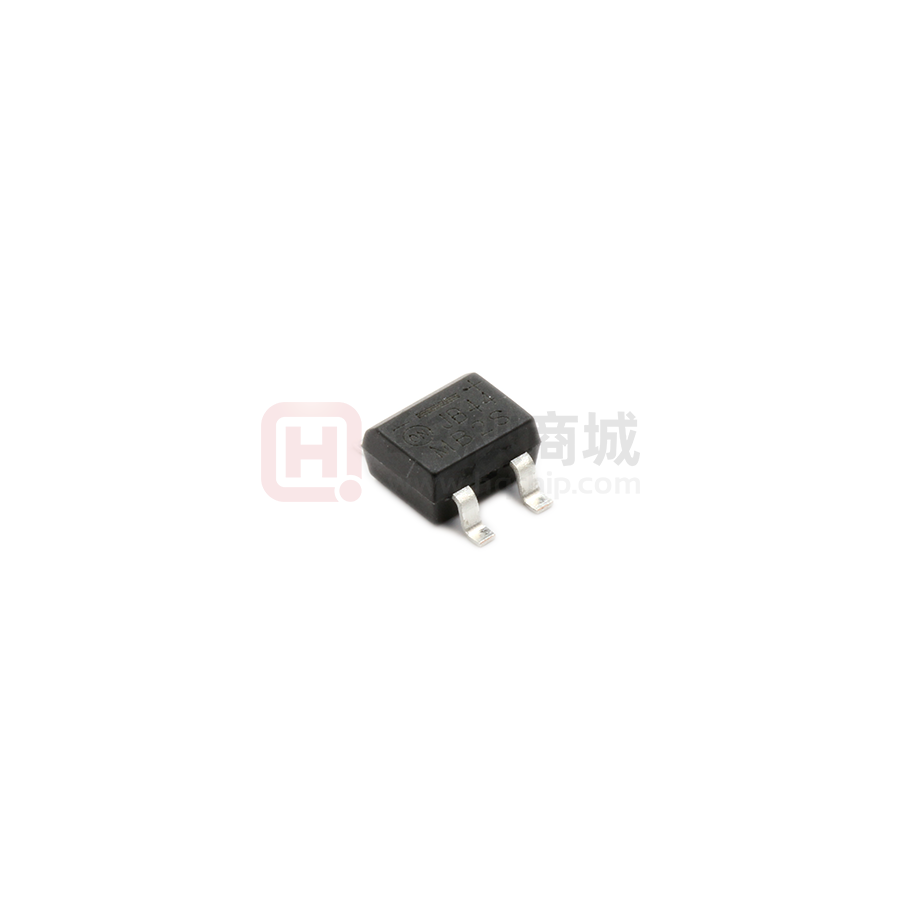
SOIC-4
IFSM rating and a 5.0 A2Sec I2T rating. Devices in the
family are also rated to breakdown voltages of up to
1000 V. These features make the MB family ideal for
small power supplies that need a little extra surge capability.
For higher IFAV current ratings, lower profile packaging,
or lower VF values, explore the ON Semiconductor
MDB family of bridge rectifiers. For improved VF and
efficiency values in the MB package or even higher
surge capability, ask about ON Semiconductor’s
pending MBxSV family.
3
~
+
~
+
+
~
~2
1
Polarity symbols molded
or mark on body
Ordering Informations
Part Number
Marking
MB1S
MB1S
MB2S
MB2S
MB4S
MB4S
MB6S
MB6S
MB8S
MB8S
© 2007 Semiconductor Components Industries, LLC.
October-2017, Rev. 2
1
Package
Packing Method
SOIC-4
Tape and Reel
Publication Order Number:
MB8S/D
MB1S - MB8S — 0.5 A Bridge Rectifiers
MB1S - MB8S
0.5 A Bridge Rectifiers
�Stresses exceeding the absolute maximum ratings may damage the device. The device may not function or be operable above the recommended operating conditions and stressing the parts to these levels is not recommended. In addition, extended exposure to stresses above the recommended operating conditions may affect device reliability. The
absolute maximum ratings are stress ratings only. Values are at TA = 25°C unless otherwise noted.
Symbol
Value
Parameter
MB1S MB2S MB4S MB6S MB8S
Unit
VRRM
Maximum Repetitive Reverse Voltage
100
200
400
600
800
V
VRMS
Maximum RMS Bridge Input Voltage
70
140
280
420
560
V
DC Reverse Voltage (Rated VR)
100
200
400
600
800
V
VR
IF(AV)
Average Rectified Forward Current at TA = 50°C
0.5
A
IFSM
Non-Repetitive Peak Forward Surge Current:
8.3 ms Single Half-Sine-Wave
35
A
TSTG
Storage Temperature Range
-55 to +150
°C
Operating Junction Temperature Range
-55 to +150
°C
Value
Unit
1.4
W
85
°C/W
20
°C/W
Value
Unit
IF = 0.5 A
1.0
V
TA = 25°C
5.0
μA
TA = 125°C
0.5
mA
TJ
Thermal Characteristics
Symbol
PD
RθJA
RθJL
Parameter
Power Dissipation
Thermal Resistance, Junction to Ambient, per
Thermal Resistance, Junction to Lead, per
Leg(1)
Leg(1)
Note:
1. Device mounted on PCB with 0.5 x 0.5 inch (13 x 13 mm) lead length.
Electrical Characteristics
Values are at TA = 25°C unless otherwise specified.
Symbol
Parameter
VF
Forward Voltage, per Bridge
IR
Reverse Current, per Leg at Rated VR
2
2
Conditions
I t
I t Rating for Fusing
t < 8.3 ms
5.0
A2s
CT
Total Capacitance, per Leg
VR = 4.0 V,
f = 1.0 MHz
13
pF
www.onsemi.com
2
MB1S - MB8S — 0.5 A Bridge Rectifiers
Absolute Maximum Ratings
�Forward Current, IF [A]
10
1
0.1
0.01
0.4
35
0.8
1
1.2
Forward Voltage, VF [V]
1.4
10
30
T C = 100 º C
25
20
15
10
5
0
0.6
Figure 2. Forward Voltage Characteristics
Reverse Current, IR [mA]
Peak Forward Surge Current, IFSM [A]
Figure 1. Derating Curve for Output Rectified Current
TA = 25º C
μs
Pulse Width = 300μ
2% Duty Cycle
1
2
5
10
20
Number of Cycles at 60Hz
50
100
Figure 3. Non-Repetitive Surge Current
1
0.1
TA = 25 º C
0.01
0
20
40
60
80
100
120
140
Percent of Rated Peak Reverse Voltage [%]
Figure 4. Reverse Current vs. Reverse Voltage
www.onsemi.com
3
MB1S - MB8S — 0.5 A Bridge Rectifiers
Typical Performance Characteristics
�ON Semiconductor and
are trademarks of Semiconductor Components Industries, LLC dba ON Semiconductor or its subsidiaries in the United States and/or other countries.
ON Semiconductor owns the rights to a number of patents, trademarks, copyrights, trade secrets, and other intellectual property. A listing of ON Semiconductor’s product/patent
coverage may be accessed at www.onsemi.com/site/pdf/Patent−Marking.pdf. ON Semiconductor reserves the right to make changes without further notice to any products herein.
ON Semiconductor makes no warranty, representation or guarantee regarding the suitability of its products for any particular purpose, nor does ON Semiconductor assume any liability
arising out of the application or use of any product or circuit, and specifically disclaims any and all liability, including without limitation special, consequential or incidental damages.
Buyer is responsible for its products and applications using ON Semiconductor products, including compliance with all laws, regulations and safety requirements or standards,
regardless of any support or applications information provided by ON Semiconductor. “Typical” parameters which may be provided in ON Semiconductor data sheets and/or
specifications can and do vary in different applications and actual performance may vary over time. All operating parameters, including “Typicals” must be validated for each customer
application by customer’s technical experts. ON Semiconductor does not convey any license under its patent rights nor the rights of others. ON Semiconductor products are not
designed, intended, or authorized for use as a critical component in life support systems or any FDA Class 3 medical devices or medical devices with a same or similar classification
in a foreign jurisdiction or any devices intended for implantation in the human body. Should Buyer purchase or use ON Semiconductor products for any such unintended or unauthorized
application, Buyer shall indemnify and hold ON Semiconductor and its officers, employees, subsidiaries, affiliates, and distributors harmless against all claims, costs, damages, and
expenses, and reasonable attorney fees arising out of, directly or indirectly, any claim of personal injury or death associated with such unintended or unauthorized use, even if such
claim alleges that ON Semiconductor was negligent regarding the design or manufacture of the part. ON Semiconductor is an Equal Opportunity/Affirmative Action Employer. This
literature is subject to all applicable copyright laws and is not for resale in any manner.
PUBLICATION ORDERING INFORMATION
LITERATURE FULFILLMENT:
Literature Distribution Center for ON Semiconductor
19521 E. 32nd Pkwy, Aurora, Colorado 80011 USA
Phone: 303−675−2175 or 800−344−3860 Toll Free USA/Canada
Fax: 303−675−2176 or 800−344−3867 Toll Free USA/Canada
Email: orderlit@onsemi.com
❖
© Semiconductor Components Industries, LLC
N. American Technical Support: 800−282−9855 Toll Free
USA/Canada
Europe, Middle East and Africa Technical Support:
Phone: 421 33 790 2910
Japan Customer Focus Center
Phone: 81−3−5817−1050
ON Semiconductor Website: www.onsemi.com
Order Literature: http://www.onsemi.com/orderlit
For additional information, please contact your local
Sales Representative
www.onsemi.com
�