MBR10100MFS,
NRVB10100MFS
SWITCHMODE
Power Rectifiers
Features
• Low Power Loss / High Efficiency
• New Package Provides Capability of Inspection and Probe After
•
•
•
•
•
•
Board Mounting
Guardring for Stress Protection
Low Forward Voltage Drop
175°C Operating Junction Temperature
Wettable Flacks Option Available
NRVB Prefix for Automotive and Other Applications Requiring
Unique Site and Control Change Requirements; AEC−Q101
Qualified and PPAP Capable
These are Pb−Free Devices
http://onsemi.com
SCHOTTKY BARRIER
RECTIFIERS
10 AMPERES
100 VOLTS
5,6
1,2,3
MARKING
DIAGRAM
Mechanical Characteristics:
•
•
•
•
•
Case: Epoxy, Molded
Epoxy Meets Flammability Rating UL 94−0 @ 0.125 in.
Lead Finish: 100% Matte Sn (Tin)
Lead and Mounting Surface Temperature for Soldering Purposes:
260°C Max. for 10 Seconds
Device Meets MSL 1 Requirements
MAXIMUM RATINGS
Rating
Symbol
Value
Unit
Peak Repetitive Reverse Voltage
Working Peak Reverse Voltage
DC Blocking Voltage
VRRM
VRWM
VR
100
Average Rectified Forward Current
(Rated VR, TC = 165°C)
IF(AV)
10
Peak Repetitive Forward Current,
(Rated VR, Square Wave,
20 kHz, TC = 163°C)
IFRM
20
A
Non−Repetitive Peak Surge Current
(Surge Applied at Rated Load
Conditions Halfwave, Single
Phase, 60 Hz)
IFSM
150
A
Storage Temperature Range
Tstg
−65 to +175
°C
Operating Junction Temperature
TJ
−55 to +175
°C
Unclamped Inductive Switching
Energy (10 mH Inductor,
Non−repetitive)
EAS
75
mJ
A
1
A
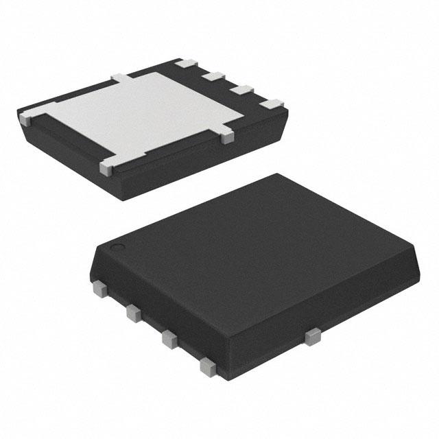
SO−8 FLAT LEAD
CASE 488AA
STYLE 2
B10100
A
Y
W
ZZ
A
C
B10100
AYWZZ
C
Not Used
= Specific Device Code
= Assembly Location
= Year
= Work Week
= Lot Traceability
V
ORDERING INFORMATION
A
Device
ESD Rating (Human Body Model)
3B
ESD Rating (Machine Model)
M4
Package
Shipping†
MBR10100MFST1G
SO−8 FL
(Pb−Free)
1500 /
Tape & Reel
MBR10100MFST3G
SO−8 FL
(Pb−Free)
5000 /
Tape & Reel
NRVB10100MFST1G
SO−8 FL
(Pb−Free)
1500 /
Tape & Reel
NRVB10100MFST3G
SO−8 FL
(Pb−Free)
5000 /
Tape & Reel
†For information on tape and reel specifications,
including part orientation and tape sizes, please
refer to our Tape and Reel Packaging Specification
Brochure, BRD8011/D.
Stresses exceeding Maximum Ratings may damage the device. Maximum
Ratings are stress ratings only. Functional operation above the Recommended
Operating Conditions is not implied. Extended exposure to stresses above the
Recommended Operating Conditions may affect device reliability.
NOTE: The heat generated must be less than the thermal conductivity from
Junction−to−Ambient: dPD/dTJ < 1/RJA.
© Semiconductor Components Industries, LLC, 2013
October, 2013 − Rev. 0
1
Publication Order Number:
MBR10100MFS/D
�MBR10100MFS, NRVB10100MFS
THERMAL CHARACTERISTICS
Characteristic
Thermal Resistance, Junction−to−Case, Steady State
(Assumes 600 mm2 1 oz. copper bond pad, on a FR4 board)
Symbol
Typ
Max
Unit
RθJC
−
1.8
°C/W
0.64
0.80
0.88
0.95
4
0.003
13
0.100
ELECTRICAL CHARACTERISTICS
Instantaneous Forward Voltage (Note 1)
(iF = 10 Amps, TJ = 125°C)
(iF = 10 Amps, TJ = 25°C)
vF
Instantaneous Reverse Current (Note 1)
(Rated dc Voltage, TJ = 125°C)
(Rated dc Voltage, TJ = 25°C)
iR
V
mA
1. Pulse Test: Pulse Width = 300 ms, Duty Cycle ≤ 2.0%.
TYPICAL CHARACTERISTICS
100
TA = 175°C
150°C
1
125°C
25°C
0.1
0
IR, INSTANTANEOUS REVERSE CURRENT (A)
iF, INSTANTANEOUS FORWARD
CURRENT (A)
10
−40°C
0.4
0.2
10
TA = 175°C
150°C
125°C
1
25°C
0.1
0.6
0.8
1.0
0
0.2
−40°C
0.4
0.8
0.6
1.0
1.2
VF, INSTANTANEOUS FORWARD VOLTAGE (V)
VF, INSTANTANEOUS FORWARD VOLTAGE (V)
Figure 1. Typical Instantaneous Forward
Characteristics
Figure 2. Maximum Instantaneous Forward
Characteristics
1.E+00
IR, INSTANTANEOUS REVERSE CURRENT (A)
iF, INSTANTANEOUS FORWARD
CURRENT (A)
100
1.E+00
1.E−01
1.E−01
TA = 175°C
1.E−02
TA = 175°C
1.E−02
1.E−03
1.E−03
TA = 125°C
1.E−04
TA = 150°C
TA = 125°C
1.E−04
1.E−05
TA = 150°C
1.E−05
TA = 25°C
1.E−06
TA = 25°C
1.E−06
1.E−07
1.E−07
1.E−08
1.E−08
1.E−09
1.E−09
TA = −40°C
1.E−10
1.E−11
TA = −40°C
1.E−10
1.E−11
0
10
20
30
40
50
60
70
80
90 100
0
10
20
30
40
50
60
70
80
90 100
VR, INSTANTANEOUS REVERSE VOLTAGE (V)
VR, INSTANTANEOUS REVERSE VOLTAGE (V)
Figure 3. Typical Reverse Characteristics
Figure 4. Maximum Reverse Characteristics
http://onsemi.com
2
�MBR10100MFS, NRVB10100MFS
TYPICAL CHARACTERISTICS
18
TJ = 25°C
100
10
RqJC = 1.8°C/W
dc
16
IF(AV), AVERAGE FORWARD
CURRENT (A)
C, JUNCTION CAPACITANCE (pF)
1,000
14
12
Square Wave
10
8
6
4
2
0
0
10
20
30
40
50
60
70
80
90
100
60
80
100
120
140
160
VR, REVERSE VOLTAGE (V)
TC, CASE TEMPERATURE (°C)
Figure 5. Typical Junction Capacitance
Figure 6. Current Derating TO−220AB
180
PF(AV), AVERAGE FORWARD POWER DISSIPATION (W)
8
IPK/IAV = 20
TJ = 175°C
7
IPK/IAV = 10
6
IPK/IAV = 5
5
4
3
Square Wave
2
dc
1
0
0
1
2
3
4
IF(AV), AVERAGE FORWARD CURRENT (A)
Figure 7. Forward Power Dissipation
100
R(t) (°C/W)
10
1
50% Duty Cycle
20%
10%
5%
2%
1%
0.1
Assumes 25°C ambient and soldered to
a 600 mm2 − oz copper pad on PCB
Single Pulse
0.01
0.001
0.000001
0.00001
0.0001
0.001
0.1
0.01
PULSE TIME (sec)
Figure 8. Thermal Response
http://onsemi.com
3
1
10
100
1,000
�MECHANICAL CASE OUTLINE
PACKAGE DIMENSIONS
DFN5 5x6, 1.27P
(SO−8FL)
CASE 488AA
ISSUE N
1
DATE 25 JUN 2018
SCALE 2:1
2X
NOTES:
1. DIMENSIONING AND TOLERANCING PER
ASME Y14.5M, 1994.
2. CONTROLLING DIMENSION: MILLIMETER.
3. DIMENSION D1 AND E1 DO NOT INCLUDE
MOLD FLASH PROTRUSIONS OR GATE
BURRS.
0.20 C
D
A
2
B
D1
2X
0.20 C
4X
E1
2
q
E
c
1
2
3
A1
4
TOP VIEW
C
DETAIL A
0.10 C
SEATING
PLANE
A
0.10 C
SIDE VIEW
MILLIMETERS
MIN
NOM
MAX
0.90
1.00
1.10
0.00
−−−
0.05
0.33
0.41
0.51
0.23
0.28
0.33
5.00
5.15
5.30
4.70
4.90
5.10
3.80
4.00
4.20
6.00
6.30
6.15
5.70
5.90
6.10
3.45
3.65
3.85
1.27 BSC
0.51
0.575
0.71
1.20
1.35
1.50
0.51
0.575
0.71
0.125 REF
3.00
3.40
3.80
0_
−−−
12 _
DIM
A
A1
b
c
D
D1
D2
E
E1
E2
e
G
K
L
L1
M
q
GENERIC
MARKING DIAGRAM*
DETAIL A
1
0.10
b
C A B
0.05
c
8X
XXXXXX
AYWZZ
e/2
e
L
1
4
K
RECOMMENDED
SOLDERING FOOTPRINT*
E2
PIN 5
(EXPOSED PAD)
L1
M
2X
0.495
4.560
2X
1.530
G
D2
2X
BOTTOM VIEW
XXXXXX = Specific Device Code
A
= Assembly Location
Y
= Year
W
= Work Week
ZZ
= Lot Traceability
*This information is generic. Please refer to
device data sheet for actual part marking.
Pb−Free indicator, “G” or microdot “ G”,
may or may not be present. Some products
may not follow the Generic Marking.
0.475
3.200
4.530
STYLE 1:
PIN 1. SOURCE
2. SOURCE
3. SOURCE
4. GATE
5. DRAIN
1.330
STYLE 2:
2X
PIN 1. ANODE
0.905
2. ANODE
3. ANODE
4. NO CONNECT
0.965
5. CATHODE
1
4X
1.000
4X 0.750
1.270
PITCH
DIMENSIONS: MILLIMETERS
*For additional information on our Pb−Free strategy and soldering
details, please download the ON Semiconductor Soldering and
Mounting Techniques Reference Manual, SOLDERRM/D.
DOCUMENT NUMBER:
DESCRIPTION:
98AON14036D
DFN5 5x6, 1.27P (SO−8FL)
Electronic versions are uncontrolled except when accessed directly from the Document Repository.
Printed versions are uncontrolled except when stamped “CONTROLLED COPY” in red.
PAGE 1 OF 1
ON Semiconductor and
are trademarks of Semiconductor Components Industries, LLC dba ON Semiconductor or its subsidiaries in the United States and/or other countries.
ON Semiconductor reserves the right to make changes without further notice to any products herein. ON Semiconductor makes no warranty, representation or guarantee regarding
the suitability of its products for any particular purpose, nor does ON Semiconductor assume any liability arising out of the application or use of any product or circuit, and specifically
disclaims any and all liability, including without limitation special, consequential or incidental damages. ON Semiconductor does not convey any license under its patent rights nor the
rights of others.
© Semiconductor Components Industries, LLC, 2018
www.onsemi.com
�onsemi,
, and other names, marks, and brands are registered and/or common law trademarks of Semiconductor Components Industries, LLC dba “onsemi” or its affiliates
and/or subsidiaries in the United States and/or other countries. onsemi owns the rights to a number of patents, trademarks, copyrights, trade secrets, and other intellectual property.
A listing of onsemi’s product/patent coverage may be accessed at www.onsemi.com/site/pdf/Patent−Marking.pdf. onsemi reserves the right to make changes at any time to any
products or information herein, without notice. The information herein is provided “as−is” and onsemi makes no warranty, representation or guarantee regarding the accuracy of the
information, product features, availability, functionality, or suitability of its products for any particular purpose, nor does onsemi assume any liability arising out of the application or use
of any product or circuit, and specifically disclaims any and all liability, including without limitation special, consequential or incidental damages. Buyer is responsible for its products
and applications using onsemi products, including compliance with all laws, regulations and safety requirements or standards, regardless of any support or applications information
provided by onsemi. “Typical” parameters which may be provided in onsemi data sheets and/or specifications can and do vary in different applications and actual performance may
vary over time. All operating parameters, including “Typicals” must be validated for each customer application by customer’s technical experts. onsemi does not convey any license
under any of its intellectual property rights nor the rights of others. onsemi products are not designed, intended, or authorized for use as a critical component in life support systems
or any FDA Class 3 medical devices or medical devices with a same or similar classification in a foreign jurisdiction or any devices intended for implantation in the human body. Should
Buyer purchase or use onsemi products for any such unintended or unauthorized application, Buyer shall indemnify and hold onsemi and its officers, employees, subsidiaries, affiliates,
and distributors harmless against all claims, costs, damages, and expenses, and reasonable attorney fees arising out of, directly or indirectly, any claim of personal injury or death
associated with such unintended or unauthorized use, even if such claim alleges that onsemi was negligent regarding the design or manufacture of the part. onsemi is an Equal
Opportunity/Affirmative Action Employer. This literature is subject to all applicable copyright laws and is not for resale in any manner.
PUBLICATION ORDERING INFORMATION
LITERATURE FULFILLMENT:
Email Requests to: orderlit@onsemi.com
onsemi Website: www.onsemi.com
◊
TECHNICAL SUPPORT
North American Technical Support:
Voice Mail: 1 800−282−9855 Toll Free USA/Canada
Phone: 011 421 33 790 2910
Europe, Middle East and Africa Technical Support:
Phone: 00421 33 790 2910
For additional information, please contact your local Sales Representative
�


 工商网监
湘ICP备2023018690号
工商网监
湘ICP备2023018690号
