ON Semiconductor
Is Now
To learn more about onsemi™, please visit our website at
www.onsemi.com
onsemi and and other names, marks, and brands are registered and/or common law trademarks of Semiconductor Components Industries, LLC dba “onsemi” or its affiliates and/or
subsidiaries in the United States and/or other countries. onsemi owns the rights to a number of patents, trademarks, copyrights, trade secrets, and other intellectual property. A listing of onsemi
product/patent coverage may be accessed at www.onsemi.com/site/pdf/Patent-Marking.pdf. onsemi reserves the right to make changes at any time to any products or information herein, without
notice. The information herein is provided “as-is” and onsemi makes no warranty, representation or guarantee regarding the accuracy of the information, product features, availability, functionality,
or suitability of its products for any particular purpose, nor does onsemi assume any liability arising out of the application or use of any product or circuit, and specifically disclaims any and all
liability, including without limitation special, consequential or incidental damages. Buyer is responsible for its products and applications using onsemi products, including compliance with all laws,
regulations and safety requirements or standards, regardless of any support or applications information provided by onsemi. “Typical” parameters which may be provided in onsemi data sheets and/
or specifications can and do vary in different applications and actual performance may vary over time. All operating parameters, including “Typicals” must be validated for each customer application
by customer’s technical experts. onsemi does not convey any license under any of its intellectual property rights nor the rights of others. onsemi products are not designed, intended, or authorized
for use as a critical component in life support systems or any FDA Class 3 medical devices or medical devices with a same or similar classification in a foreign jurisdiction or any devices intended for
implantation in the human body. Should Buyer purchase or use onsemi products for any such unintended or unauthorized application, Buyer shall indemnify and hold onsemi and its officers, employees,
subsidiaries, affiliates, and distributors harmless against all claims, costs, damages, and expenses, and reasonable attorney fees arising out of, directly or indirectly, any claim of personal injury or death
associated with such unintended or unauthorized use, even if such claim alleges that onsemi was negligent regarding the design or manufacture of the part. onsemi is an Equal Opportunity/Affirmative
Action Employer. This literature is subject to all applicable copyright laws and is not for resale in any manner. Other names and brands may be claimed as the property of others.
�MBR2H200SF
Surface Mount
Schottky Power Rectifier
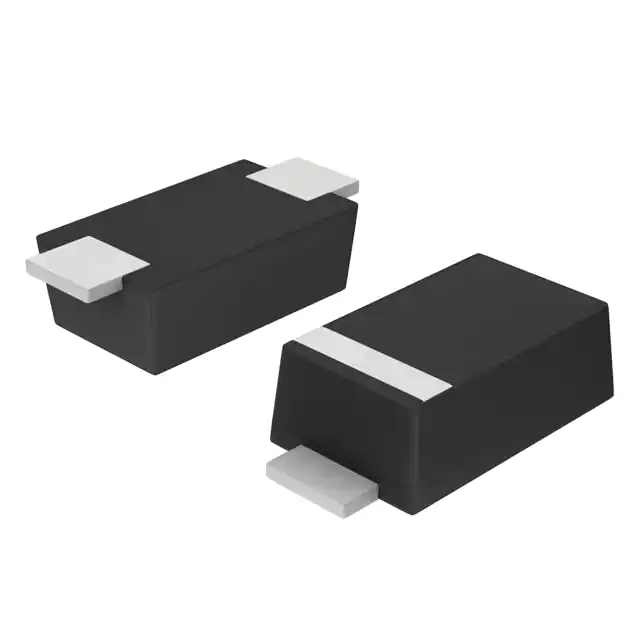
Plastic SOD−123FL Package
This device uses the Schottky Barrier principle with a large area
metal−to−silicon power diode. Ideally suited for low voltage, high
frequency rectification or as free wheeling and polarity protection
diodes in surface mount applications where compact size and weight
are critical to the system. Because of its small size, it is ideal for use in
portable and battery powered products such as cellular and cordless
phones, chargers, notebook computers, printers, PDAs and PCMCIA
cards. Typical applications are AC−DC and DC−DC converters,
reverse battery protection, and “Oring” of multiple supply voltages
and any other application where performance and size are critical.
www.onsemi.com
SCHOTTKY BARRIER
RECTIFIER
2.0 AMPERES
200 VOLTS
Features
•
•
•
•
•
Guardring for Stress Protection
Low Forward Voltage
Epoxy Meets UL 94 V−0
Package Designed for Optimal Automated Board Assembly
These are Pb−Free Devices
SOD−123FL
CASE 498
MARKING DIAGRAM
Mechanical Characteristics
•
•
•
•
•
•
•
•
Reel Options: MBR2H200SFT3G = 10,000 per 13 in reel/8 mm tape
Device Marking: L2J
Polarity Designator: Cathode Band
Weight: 11.7 mg (approximately)
Case: Epoxy, Molded
Lead Finish: 100% Matte Sn (Tin)
Lead and Mounting Surface Temperature for Soldering Purposes:
260°C Max. for 10 Seconds
Device Meets MSL 1 Requirements
L2JMG
G
L2J
= Specific Device Code
M
= Date Code
G
= Pb−Free Package
(Note: Microdot may be in either location)
ORDERING INFORMATION
Device
Package
Shipping†
MBR2H200SFT1G
SOD−123
(Pb−Free)
3000 / Tape &
Reel
MBR2H200SFT3G
SOD−123
(Pb−Free)
10000 / Tape &
Reel
†For information on tape and reel specifications,
including part orientation and tape sizes, please
refer to our Tape and Reel Packaging Specification
Brochure, BRD8011/D.
© Semiconductor Components Industries, LLC, 2017
January, 2017 − Rev. 1
1
Publication Order Number:
MBR2H200SF/D
�MBR2H200SF
MAXIMUM RATINGS
Rating
Symbol
Value
Unit
VRRM
VRWM
VR
200
V
IO
2.0
A
Peak Repetitive Forward Current
(Rated VR, Square Wave, 20 kHz, TC = 105°C)
IFRM
4.0
A
Non−Repetitive Peak Surge Current
(Surge Applied at Rated Load Conditions Halfwave, Single Phase, 60 Hz)
IFSM
30
A
Tstg, TJ
−55 to +150
°C
Peak Repetitive Reverse Voltage
Working Peak Reverse Voltage
DC Blocking Voltage
Average Rectified Forward Current
(TL = 108°C)
Storage and Operating Junction Temperature Range (Note 1)
Stresses exceeding those listed in the Maximum Ratings table may damage the device. If any of these limits are exceeded, device functionality
should not be assumed, damage may occur and reliability may be affected.
1. The heat generated must be less than the thermal conductivity from
Junction−to−Ambient: dPD/dTJ < 1/RqJA.
THERMAL CHARACTERISTICS
Characteristic
Symbol
Value
Unit
Thermal Resistance, Junction−to−Lead (Note 2)
YJCL
23
°C/W
Thermal Resistance, Junction−to−Ambient (Note 2)
RqJA
85
°C/W
Thermal Resistance, Junction−to−Ambient (Note 3)
RqJA
330
°C/W
Symbol
Value
Unit
ELECTRICAL CHARACTERISTICS
Characteristic
Maximum Instantaneous Forward Voltage (Note 4)
(IF = 1.0 A, TJ = 25°C)
(IF = 2.0 A, TJ = 25°C)
(IF = 1.0 A, TJ = 125°C)
(IF = 2.0 A, TJ = 125°C)
VF
Maximum Instantaneous Reverse Current (Note 4)
(Rated dc Voltage, TJ = 25°C)
(Rated dc Voltage, TJ = 125°C)
IR
V
0.86
0.94
0.71
0.78
200
2
mA
mA
Product parametric performance is indicated in the Electrical Characteristics for the listed test conditions, unless otherwise noted. Product
performance may not be indicated by the Electrical Characteristics if operated under different conditions.
2. Mounted with 700 mm2 copper pad size (Approximately 1 in2) 1 oz FR4 Board.
3. Mounted with pad size approximately 20 mm2 copper, 1 oz FR4 Board.
4. Pulse Test: Pulse Width ≤ 380 ms, Duty Cycle ≤ 2.0%.
www.onsemi.com
2
�MBR2H200SF
TYPICAL CHARACTERISTICS
TL = 150°C
10
TL = 25°C
iF, INSTANTANEOUS FORWARD
CURRENT (A)
iF, INSTANTANEOUS FORWARD
CURRENT (A)
10
TL = −55°C
TL = 125°C
1
TL = 25°C
TL = −55°C
TL = 125°C
1
0.1
0.1
0.2
0.4
0.6
0.8
1.0
1.2
1.4
1.6
1.8
0
2.0
0.4
0.6
0.8
1.0
1.2
1.6
1.4
1.8 2.0
VF, INSTANTANEOUS FORWARD VOLTAGE (V)
Figure 1. Typical Instantaneous Forward
Characteristics
Figure 2. Maximum Instantaneous Forward
Characteristics
1.E−03
1.E−01
TL = 150°C
1.E−04
1.E−05
TL = 150°C
1.E−02
1.E−03
TL = 125°C
TL = 125°C
1.E−04
1.E−06
1.E−07
1.E−05
1.E−08
1.E−06
1.E−09
TL = 25°C
1.E−07
TL = 25°C
1.E−10
TL = −55°C
1.E−08
TL = −55°C
1.E−11
20
40
60
80
1.E−09
100 120 140 160 180 200
0
20
40
60
80
100 120 140 160 180 200
VR, INSTANTANEOUS REVERSE VOLTAGE (V)
VR, INSTANTANEOUS REVERSE VOLTAGE (V)
Figure 3. Typical Reverse Characteristics
Figure 4. Maximum Reverse Characteristics
IF(AV), AVERAGE FORWARD CURRENT (A)
0
100
TL = 25°C
10
1
1
0.2
VF, INSTANTANEOUS FORWARD VOLTAGE (V)
IR, INSTANTANEOUS REVERSE CURRENT (A)
IR, INSTANTANEOUS REVERSE CURRENT (A)
0
C, JUNCTION CAPACITANCE (pF)
TL = 150°C
10
100
4.0
3.5
RqJL = 23°C/W
DC
3.0
2.5
Square Wave
2.0
1.5
1.0
0.5
0
0
20
40
60
80
100
120
VR, REVERSE VOLTAGE (V)
TL, LEAD TEMPERATURE (°C)
Figure 5. Typical Junction Capacitance
Figure 6. Current Derating per Diode
www.onsemi.com
3
140
�MBR2H200SF
TYPICAL CHARACTERISTICS
5
PF(AV), AVERAGE FORWARD
POWER DISSIPATION (W)
TJ = 150°C
IPK/IAV = 20
4
IPK/IAV = 10
3
IPK/IAV = 5
2
DC
1
Square Wave
0
0
0.5
1.0
1.5
2.0
IF(AV), AVERAGE FORWARD CURRENT (A)
Figure 7. Forward Power Dissipation
1000
R(t) (C/W)
100
10
50% (DUTY CYCLE)
25%
10%
5.0%
2.0%
1.0%
1.0
0.1
SINGLE PULSE
0.01
0.000001
0.00001
0.0001
0.001
0.01
0.1
1.0
10
100
1000
10
100
1000
PULSE TIME (s)
Figure 8. Thermal Response, Junction−to−Ambient (20 mm2 pad)
100
50% (DUTY CYCLE)
25%
R(t) (C/W)
10
10%
5.0%
2.0%
1.0
1.0%
0.1
SINGLE PULSE
0.01
0.000001
0.00001
0.0001
0.001
0.01
0.1
1.0
PULSE TIME (s)
Figure 9. Thermal Response, Junction−to−Ambient (1 in2 pad)
www.onsemi.com
4
�MECHANICAL CASE OUTLINE
PACKAGE DIMENSIONS
SOD−123FL
CASE 498
ISSUE D
DATE 10 MAY 2013
SCALE 4:1
E
D
q
1
NOTES:
1. DIMENSIONING AND TOLERANCING PER ANSI Y14.5M, 1982.
2. CONTROLLING DIMENSION: MILLIMETER.
3. DIMENSIONS A AND B DO NOT INCLUDE MOLD FLASH.
4. DIMENSIONS D AND J ARE TO BE MEASURED ON FLAT SECTION
OF THE LEAD: BETWEEN 0.10 AND 0.25 MM FROM THE LEAD TIP.
2
POLARITY INDICATOR
OPTIONAL AS NEEDED
A
END VIEW
TOP VIEW
q
HE
SIDE VIEW
2X
b
INCHES
NOM
0.037
0.002
0.035
0.006
0.065
0.106
0.030
0.142
−
MAX
0.039
0.004
0.043
0.008
0.071
0.114
0.037
0.150
8°
(Note: Microdot may be in either location)
4.20
ÉÉÉ
ÉÉÉ
ÉÉÉ
ÉÉÉ
MIN
0.035
0.000
0.028
0.004
0.059
0.098
0.022
0.134
0°
XXX = Specific Device Code
M = Date Code
G
= Pb−Free Package
RECOMMENDED
SOLDERING FOOTPRINT*
1.22
MILLIMETERS
NOM
MAX
0.95
0.98
0.05
0.10
0.90
1.10
0.15
0.20
1.65
1.80
2.70
2.90
0.75
0.95
3.60
3.80
8°
−
XXXMG
G
L
BOTTOM VIEW
2X
MIN
0.90
0.00
0.70
0.10
1.50
2.50
0.55
3.40
0°
GENERIC
MARKING DIAGRAM*
c
2X
A1
DIM
A
A1
b
c
D
E
L
HE
q
*This information is generic. Please refer to
device data sheet for actual part marking.
Pb−Free indicator, “G” or microdot “ G”,
may or may not be present.
2X
ÉÉÉÉ
ÉÉÉÉ
ÉÉÉÉ
ÉÉÉÉ
1.25
DIMENSIONS: MILLIMETERS
*For additional information on our Pb−Free strategy and soldering
details, please download the ON Semiconductor Soldering and
Mounting Techniques Reference Manual, SOLDERRM/D.
DOCUMENT NUMBER:
DESCRIPTION:
98AON11184D
SOD−123FL
Electronic versions are uncontrolled except when accessed directly from the Document Repository.
Printed versions are uncontrolled except when stamped “CONTROLLED COPY” in red.
PAGE 1 OF 1
ON Semiconductor and
are trademarks of Semiconductor Components Industries, LLC dba ON Semiconductor or its subsidiaries in the United States and/or other countries.
ON Semiconductor reserves the right to make changes without further notice to any products herein. ON Semiconductor makes no warranty, representation or guarantee regarding
the suitability of its products for any particular purpose, nor does ON Semiconductor assume any liability arising out of the application or use of any product or circuit, and specifically
disclaims any and all liability, including without limitation special, consequential or incidental damages. ON Semiconductor does not convey any license under its patent rights nor the
rights of others.
© Semiconductor Components Industries, LLC, 2019
www.onsemi.com
�ON Semiconductor and
are trademarks of Semiconductor Components Industries, LLC dba ON Semiconductor or its subsidiaries in the United States and/or other countries.
ON Semiconductor owns the rights to a number of patents, trademarks, copyrights, trade secrets, and other intellectual property. A listing of ON Semiconductor’s product/patent
coverage may be accessed at www.onsemi.com/site/pdf/Patent−Marking.pdf. ON Semiconductor reserves the right to make changes without further notice to any products herein.
ON Semiconductor makes no warranty, representation or guarantee regarding the suitability of its products for any particular purpose, nor does ON Semiconductor assume any liability
arising out of the application or use of any product or circuit, and specifically disclaims any and all liability, including without limitation special, consequential or incidental damages.
Buyer is responsible for its products and applications using ON Semiconductor products, including compliance with all laws, regulations and safety requirements or standards,
regardless of any support or applications information provided by ON Semiconductor. “Typical” parameters which may be provided in ON Semiconductor data sheets and/or
specifications can and do vary in different applications and actual performance may vary over time. All operating parameters, including “Typicals” must be validated for each customer
application by customer’s technical experts. ON Semiconductor does not convey any license under its patent rights nor the rights of others. ON Semiconductor products are not
designed, intended, or authorized for use as a critical component in life support systems or any FDA Class 3 medical devices or medical devices with a same or similar classification
in a foreign jurisdiction or any devices intended for implantation in the human body. Should Buyer purchase or use ON Semiconductor products for any such unintended or unauthorized
application, Buyer shall indemnify and hold ON Semiconductor and its officers, employees, subsidiaries, affiliates, and distributors harmless against all claims, costs, damages, and
expenses, and reasonable attorney fees arising out of, directly or indirectly, any claim of personal injury or death associated with such unintended or unauthorized use, even if such
claim alleges that ON Semiconductor was negligent regarding the design or manufacture of the part. ON Semiconductor is an Equal Opportunity/Affirmative Action Employer. This
literature is subject to all applicable copyright laws and is not for resale in any manner.
PUBLICATION ORDERING INFORMATION
LITERATURE FULFILLMENT:
Email Requests to: orderlit@onsemi.com
ON Semiconductor Website: www.onsemi.com
◊
TECHNICAL SUPPORT
North American Technical Support:
Voice Mail: 1 800−282−9855 Toll Free USA/Canada
Phone: 011 421 33 790 2910
www.onsemi.com
1
Europe, Middle East and Africa Technical Support:
Phone: 00421 33 790 2910
For additional information, please contact your local Sales Representative
�