Surface Mount
Schottky Power Rectifier
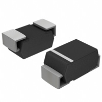
SMA Power Surface Mount Package
MBRA210L, NRVBA210L,
NRVBA210LN
This device employs the Schottky Barrier principle in a
metal−to−silicon power rectifier. Features epitaxial construction with
oxide passivation and metal overlay contact. Ideally suited for low
voltage, high frequency switching power supplies; free wheeling
diodes and polarity protection diodes. Typical applications are
AC−DC and DC−DC converters, reverse battery protection, and
“Oring” of multiple supply voltages and any other application where
performance and size are critical.
www.onsemi.com
SCHOTTKY BARRIER
RECTIFIER
2 AMPERES
10 VOLTS
Features
•
•
•
•
•
•
•
•
Ultra Low VF
1st in the Market Place with a 10 VR Schottky Rectifier
Compact Package with J−Bend Leads Ideal for Automated Handling
Highly Stable Oxide Passivated Junction
Guardring for Over−Voltage Protection
Optimized for Low Forward Voltage
NRVBA Prefix for Automotive and Other Applications Requiring
Unique Site and Control Change Requirements; AEC−Q101
Qualified and PPAP Capable*
These Devices are Pb−Free, Halogen Free/BFR Free and are RoHS
Compliant
Mechanical Characteristics:
•
•
•
•
•
•
•
Case: Molded Epoxy
Epoxy Meets UL 94 V−0 @ 0.125 in
Weight: 70 mg (Approximately)
Finish: All External Surfaces Corrosion Resistant and Terminal
Leads are Readily Solderable
Lead and Mounting Surface Temperature for Soldering Purposes:
260°C Max. for 10 Seconds
Polarity: Polarity Band Indicates Cathode Lead
ESD Ratings:
♦ Machine Model = C
♦ Human Body Model = 3A
SMA
CASE 403D
MARKING DIAGRAM
B2L1
AYWW
G
B2L1 = Specific Device Code
A
= Assembly Location**
Y
= Year
WW = Work Week
G
= Pb−Free Package
(Note: Microdot may be in either location)
**The Assembly Location code (A) is front side
optional. In cases where the Assembly Location is
stamped in the package bottom (molding ejecter pin),
the front side assembly code may be blank.
ORDERING INFORMATION
Device
Package
Shipping†
MBRA210LT3G
SMA
(Pb−Free)
5,000 /
Tape & Reel
NRVBA210LT3G*
SMA
(Pb−Free)
5,000 /
Tape & Reel
NRVBA210LNT3G*
SMA
(Pb−Free)
5,000 /
Tape & Reel
†For information on tape and reel specifications,
including part orientation and tape sizes, please
refer to our Tape and Reel Packaging Specification
Brochure, BRD8011/D.
© Semiconductor Components Industries, LLC, 2012
December, 2019 − Rev. 7
1
Publication Order Number:
MBRA210LT3/D
�MBRA210L, NRVBA210L, NRVBA210LN
MAXIMUM RATINGS
Rating
Symbol
Value
Unit
VRRM
VRWM
VR
10
V
Peak Repetitive Reverse Voltage
Working Peak Reverse Voltage
DC Blocking Voltage
Average Rectified Forward Current
(At Rated VR, TL = 110°C)
IO
Non−Repetitive Peak Surge Current
(Surge Applied at Rated Load Conditions Halfwave, Single Phase, 60 Hz)
IFSM
Storage/Operating Case Temperature
Operating Junction Temperature
A
160
Tstg, TC
TJ
Voltage Rate of Change
(Rated VR, TJ = 25°C)
A
2.0
−55 to +125
dv/dt
°C
V/ms
10,000
Stresses exceeding those listed in the Maximum Ratings table may damage the device. If any of these limits are exceeded, device functionality
should not be assumed, damage may occur and reliability may be affected.
THERMAL CHARACTERISTICS
Characteristic
Thermal Resistance, Junction−to−Lead
Thermal Resistance, Junction−to−Ambient
Symbol
Min Pad
1 Inch Pad
Unit
RqJL
RqJA
22
150
15
81
°C/W
VF
TJ = 25°C
TJ = 100°C
V
0.260
0.325
0.350
0.15
0.23
0.26
TJ = 25°C
TJ = 100°C
0.25
0.70
40
60
ELECTRICAL CHARACTERISTICS
Maximum Instantaneous Forward Voltage (Note 1)
(IF = 0.1 A)
(IF = 1.0 A)
(IF = 2.0 A)
Maximum Instantaneous Reverse Current
IR
(VR = 5.0 V)
(VR = 10 V)
mA
Product parametric performance is indicated in the Electrical Characteristics for the listed test conditions, unless otherwise noted. Product
performance may not be indicated by the Electrical Characteristics if operated under different conditions.
1. Pulse Test: Pulse Width ≤ 250 ms, Duty Cycle ≤ 2%.
100
VF @ 125°C
10
25°C
100°C
75°C
1
0.1
0.05 0.1
0.15
0.2
0.25
0.3
0.35
0.4
IF, MAXIMUM INSTANTANEOUS
FORWARD CURRENT (AMPS)
IF, INSTANTANEOUS FORWARD
CURRENT (AMPS)
100
VF @ 125°C
10
100°C
75°C
1
0.1
0.45
25°C
0.05
0.15
0.25
0.35
0.45
VF, MAXIMUM INSTANTANEOUS FORWARD
VOLTAGE (VOLTS)
VF, INSTANTANEOUS FORWARD VOLTAGE (VOLTS)
Figure 1. Typical Forward Voltage
Figure 2. Maximum Forward Voltage
www.onsemi.com
2
0.55
�MBRA210L, NRVBA210L, NRVBA210LN
IR, REVERSE CURRENT (AMPS)
1.0E−01
IR @ 125°C
100°C
1.0E−02
75°C
1.0E−03
1.0E−04
1.0E−05
25°C
0
2
4
6
8
10
VR, REVERSE VOLTAGE (VOLTS)
3.5
RATED VOLTAGE
APPLIED
RqJL = 22 °C/W
TJ = 125°C
3
2.5
SQUARE WAVE
2
1.5
1
0.5
0
90
95
100
105
110
115
120
125
130
TL, LEAD TEMPERATURE (°C)
0.9
TJ = 125°C
0.8
dc
0.7
0.6
SQUARE WAVE
0.5
0.4
0.3
0.2
0.1
0
0
0.5
1
1.5
25°C
f = 1 MHz
1000
0
1
2
3
4
2.5
3
Figure 5. Forward Power Dissipation
10,000
100
2
IF(AV), AVERAGE FORWARD CURRENT (AMPS)
Figure 4. Current Derating − Junction to Lead
C, CAPACITANCE (pF)
IF, AVERAGE FORWARD
CURRENT (AMPS)
dc
PFO, AVERAGE POWER DISSIPATION (WATTS)
Figure 3. Typical Reverse Current
5
6
7
8
VR, REVERSE VOLTAGE (VOLTS)
Figure 6. Typical Capacitance
www.onsemi.com
3
9
10
3.5
�R(t), TRANSIENT THERMAL RESISTANCE (°C/W)
MBRA210L, NRVBA210L, NRVBA210LN
100
D = 0.5
0.2
0.1
10
0.05
0.02
0.01
1
SINGLE PULSE
0.1
0.00001
0.0001
0.001
0.01
0.1
1
10
100
1000
100
1000
t, TIME (S)
R(t), TRANSIENT THERMAL RESISTANCE (°C/W)
Figure 7. Thermal Response, Junction to Ambient (min pad)
100
D = 0.5
0.2
10
0.1
0.05
0.02
1
0.1
0.01
SINGLE PULSE
0.00001
0.0001
0.001
0.01
0.1
1
10
t, TIME (S)
Figure 8. Thermal Response, Junction to Ambient (1 inch pad)
www.onsemi.com
4
�MECHANICAL CASE OUTLINE
PACKAGE DIMENSIONS
STYLE 1
SMA
CASE 403D
ISSUE J
STYLE 2
SCALE 1:1
STYLE 1:
PIN 1. CATHODE (POLARITY BAND)
2. ANODE
DATE 22 OCT 2021
STYLE 2:
NO POLARITY
GENERIC
MARKING DIAGRAM*
xxxx
AYWWG
STYLE 1
xxxx
A
Y
WW
G
xxxx
AYWWG
STYLE 2
= Specific Device Code
= Assembly Location
= Year
= Work Week
= Pb−Free Package
*This information is generic. Please refer to
device data sheet for actual part marking.
Pb−Free indicator, “G” or microdot “G”, may
or may not be present. Some products may
not follow the Generic Marking.
DOCUMENT NUMBER:
DESCRIPTION:
98AON04079D
SMA
Electronic versions are uncontrolled except when accessed directly from the Document Repository.
Printed versions are uncontrolled except when stamped “CONTROLLED COPY” in red.
PAGE 1 OF 1
onsemi and
are trademarks of Semiconductor Components Industries, LLC dba onsemi or its subsidiaries in the United States and/or other countries. onsemi reserves
the right to make changes without further notice to any products herein. onsemi makes no warranty, representation or guarantee regarding the suitability of its products for any particular
purpose, nor does onsemi assume any liability arising out of the application or use of any product or circuit, and specifically disclaims any and all liability, including without limitation
special, consequential or incidental damages. onsemi does not convey any license under its patent rights nor the rights of others.
© Semiconductor Components Industries, LLC, 2019
www.onsemi.com
�onsemi,
, and other names, marks, and brands are registered and/or common law trademarks of Semiconductor Components Industries, LLC dba “onsemi” or its affiliates
and/or subsidiaries in the United States and/or other countries. onsemi owns the rights to a number of patents, trademarks, copyrights, trade secrets, and other intellectual property.
A listing of onsemi’s product/patent coverage may be accessed at www.onsemi.com/site/pdf/Patent−Marking.pdf. onsemi reserves the right to make changes at any time to any
products or information herein, without notice. The information herein is provided “as−is” and onsemi makes no warranty, representation or guarantee regarding the accuracy of the
information, product features, availability, functionality, or suitability of its products for any particular purpose, nor does onsemi assume any liability arising out of the application or use
of any product or circuit, and specifically disclaims any and all liability, including without limitation special, consequential or incidental damages. Buyer is responsible for its products
and applications using onsemi products, including compliance with all laws, regulations and safety requirements or standards, regardless of any support or applications information
provided by onsemi. “Typical” parameters which may be provided in onsemi data sheets and/or specifications can and do vary in different applications and actual performance may
vary over time. All operating parameters, including “Typicals” must be validated for each customer application by customer’s technical experts. onsemi does not convey any license
under any of its intellectual property rights nor the rights of others. onsemi products are not designed, intended, or authorized for use as a critical component in life support systems
or any FDA Class 3 medical devices or medical devices with a same or similar classification in a foreign jurisdiction or any devices intended for implantation in the human body. Should
Buyer purchase or use onsemi products for any such unintended or unauthorized application, Buyer shall indemnify and hold onsemi and its officers, employees, subsidiaries, affiliates,
and distributors harmless against all claims, costs, damages, and expenses, and reasonable attorney fees arising out of, directly or indirectly, any claim of personal injury or death
associated with such unintended or unauthorized use, even if such claim alleges that onsemi was negligent regarding the design or manufacture of the part. onsemi is an Equal
Opportunity/Affirmative Action Employer. This literature is subject to all applicable copyright laws and is not for resale in any manner.
PUBLICATION ORDERING INFORMATION
LITERATURE FULFILLMENT:
Email Requests to: orderlit@onsemi.com
onsemi Website: www.onsemi.com
◊
TECHNICAL SUPPORT
North American Technical Support:
Voice Mail: 1 800−282−9855 Toll Free USA/Canada
Phone: 011 421 33 790 2910
Europe, Middle East and Africa Technical Support:
Phone: 00421 33 790 2910
For additional information, please contact your local Sales Representative
�