MBRM120E
Surface Mount
Schottky Power Rectifier
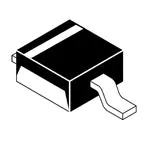
POWERMITE
Power Surface Mount Package
The Schottky Powermite employs the Schottky Barrier principle
with a barrier metal and epitaxial construction that produces optimal
forward voltage drop–reverse current tradeoff. The advanced
packaging techniques provide for a highly efficient micro miniature,
space saving surface mount Rectifier. With its unique heatsink design,
the Powermite has the same thermal performance as the SMA while
being 50% smaller in footprint area, and delivering one of the lowest
height profiles, < 1.1 mm in the industry. Because of its small size, it is
ideal for use in portable and battery powered products such as cellular
and cordless phones, chargers, notebook computers, printers, PDAs
and PCMCIA cards. Typical applications are ac/dc and dc–dc
converters, reverse battery protection, and “Oring” of multiple supply
voltages and any other application where performance and size are
critical.
http://onsemi.com
SCHOTTKY BARRIER
RECTIFIER
1.0 AMPERES
20 VOLTS
ANODE
CATHODE
Features:
•
•
•
•
•
Low Profile – Maximum Height of 1.1 mm
Small Footprint – Footprint Area of 8.45 mm2
Low VF Provides Higher Efficiency and Extends Battery Life
Supplied in 12 mm Tape and Reel
Low Thermal Resistance with Direct Thermal Path of Die on
Exposed Cathode Heat Sink
POWERMITE
CASE 457
PLASTIC
MARKING DIAGRAM
Mechanical Characteristics:
•
•
•
•
•
•
M
BCV
Powermite is JEDEC Registered as DO–216AA
Case: Molded Epoxy
Epoxy Meets UL94V–0 at 1/8″
Weight: 62 mg (approximately)
Device Marking: BCV
Lead and Mounting Surface Temperature for Soldering Purposes.
260°C Maximum for 10 Seconds
BCV
M
= Device Code
= Date Code
ORDERING INFORMATION
Device
MAXIMUM RATINGS
Package
MBRM120ET1 POWERMITE
Please See the Table on the Following Page
Shipping
3000/Tape & Reel
MBRM120ET3 POWERMITE 12,000/Tape & Reel
Semiconductor Components Industries, LLC, 2001
November, 2001 – Rev. 0
1
Publication Order Number:
MBRM120E/D
�MBRM120E
MAXIMUM RATINGS
Rating
Symbol
Value
Unit
VRRM
VRWM
VR
20
V
IO
1.0
A
Peak Repetitive Forward Current
(At Rated VR, Square Wave, 20 kHz, TC = 135°C)
IFRM
2.0
A
Non–Repetitive Peak Surge Current
(Non–Repetitive peak surge current, halfwave, single phase, 60 Hz)
IFSM
50
A
Storage Temperature
Tstg
–65 to 150
°C
TJ
–65 to 150
°C
dv/dt
10,000
V/�s
Rtjl
Rtjtab
Rtja
35
23
277
°C/W
Peak Repetitive Reverse Voltage
Working Peak Reverse Voltage
DC Blocking Voltage
Average Rectified Forward Current (At Rated VR, TC = 130°C)
Operating Junction Temperature
Voltage Rate of Change (Rated VR, TJ = 25°C)
THERMAL CHARACTERISTICS
Thermal Resistance – Junction–to–Lead (Anode) (Note 1)
Thermal Resistance – Junction–to–Tab (Cathode) (Note 1)
Thermal Resistance – Junction–to–Ambient (Note 1)
1. Mounted with minimum recommended pad size, PC Board FR4, See Figures 9 and 10.
ELECTRICAL CHARACTERISTICS
VF
Maximum Instantaneous Forward Voltage (Note 2), See Figure 2
(IF = 0.1 A)
(IF = 1.0 A)
(IF = 2.0 A)
IR
Maximum Instantaneous Reverse Current (Note 2), See Figure 4
(VR = 20 V)
(VR = 10 V)
(VR = 5.0 V)
2. Pulse Test: Pulse Width ≤ 250 µs, Duty Cycle ≤ 2%.
http://onsemi.com
2
TJ = 25°C
TJ = 100°C
0.455
0.530
0.595
0.360
0.455
0.540
TJ = 25°C
TJ = 100°C
10
1.0
0.5
1600
500
300
V
�A
�iF, INSTANTANEOUS FORWARD CURRENT (AMPS)
iF, INSTANTANEOUS FORWARD CURRENT (AMPS)
MBRM120E
10
TJ = 150°C
TJ = 25°C
TJ = 100°C
TJ = –40°C
1.0
0.1
0.2
0.4
0.6
0.8
vF, INSTANTANEOUS FORWARD VOLTAGE (VOLTS)
10
TJ = 150°C
TJ = 100°C
1.0
TJ = 25°C
0.1
0.2
0.6
0.8
Figure 2. Maximum Forward Voltage
100E–3
IR, MAXIMUM REVERSE CURRENT (AMPS)
Figure 1. Typical Forward Voltage
IR, REVERSE CURRENT (AMPS)
0.4
VF, MAXIMUM INSTANTANEOUS FORWARD VOLTAGE
(VOLTS)
100E–3
10E–3
1E–3
TJ = 150°C
100E–6
TJ = 100°C
1E–6
TJ = 25°C
5.0
10
1E–3
TJ = 100°C
10E–6
TJ = 25°C
1E–6
100E–9
10E–9
0
TJ = 150°C
100E–6
10E–6
100E–9
10E–3
20
15
10E–9
0
5.0
10
15
VR, REVERSE VOLTAGE (VOLTS)
VR, REVERSE VOLTAGE (VOLTS)
Figure 3. Typical Reverse Current
Figure 4. Maximum Reverse Current
http://onsemi.com
3
20
�FREQ = 20 kHz
dc
1.6
PFO, AVERAGE DISSIPATION (WATTS)
1.8
1.4
SQUARE WAVE
1.2
1.0
Ipk/Io = �
0.8
Ipk/Io = 5
0.6
Ipk/Io = 10
0.4
Ipk/Io = 20
0.2
0
25
45
65
85
105
125
145
dc
0.6
Ipk/Io = �
SQUARE
WAVE
0.5
Ipk/Io = 5
0.4
Ipk/Io = 10
0.3
Ipk/Io = 20
0.2
0.1
0
0
165
0.2
0.4
0.6
0.8
1.0
1.2
1.4
TL, LEAD TEMPERATURE (°C)
IO, AVERAGE FORWARD CURRENT (AMPS)
Figure 5. Current Derating
Figure 6. Forward Power Dissipation
1000
C, CAPACITANCE (pF)
0.7
TJ, DERATED OPERATING TEMPERATURE
(�C)
IO, AVERAGE FORWARD CURRENT (AMPS)
MBRM120E
1.6
150
TJ = 25°C
Rtja = 33.72°C/W
51°C/W
148
100
69°C/W
83.53°C/W
96°C/W
146
10
144
0
2.0
4.0
6.0
8.0
10
12
14
16
18
20
0
2.0
4.0
6.0
8.0
10
12
14
16
18
20
VR, REVERSE VOLTAGE (VOLTS)
VR, DC REVERSE VOLTAGE (VOLTS)
Figure 7. Capacitance
Figure 8. Typical Operating Temperature Derating*
* Reverse power dissipation and the possibility of thermal runaway must be considered when operating this device under any reverse voltage conditions. Calculations of TJ therefore must include forward and reverse power effects. The allowable operating
TJ may be calculated from the equation:
TJ = TJmax – r(t)(Pf + Pr) where
r(t) = thermal impedance under given conditions,
Pf = forward power dissipation, and
Pr = reverse power dissipation
This graph displays the derated allowable TJ due to reverse bias under DC conditions only and is calculated as TJ = TJmax – r(t)Pr,
where r(t) = Rthja. For other power applications further calculations must be performed.
http://onsemi.com
4
�R(T), TRANSIENT THERMAL RESISTANCE (NORMALIZED)
MBRM120E
1.0
50%
20%
0.1
10%
5.0%
0.01
2.0%
1.0%
Rtjl(t) = Rtjl*r(t)
R(T), TRANSIENT THERMAL RESISTANCE (NORMALIZED)
0.001
0.00001
0.0001
0.001
0.01
0.1
1.0
10
100
T, TIME (s)
Figure 9. Thermal Response Junction to Lead
1.0
50%
20%
0.1
10%
5.0%
0.01
2.0%
1.0%
0.001
0.00001
Rtjl(t) = Rtjl*r(t)
0.0001
0.001
0.01
0.1
1.0
10
T, TIME (s)
Figure 10. Thermal Response Junction to Ambient
0.025
0.635
0.105
2.67
0.030
0.762
0.100
2.54
0.050
1.27
inches
mm
Minimum Recommended Footprint
http://onsemi.com
5
100
1,000
�MBRM120E
PACKAGE DIMENSIONS
POWERMITE
PLASTIC PACKAGE
CASE 457–04
ISSUE D
F
0.08 (0.003)
C
–A–
J
M
T B
S
TERM. 1
–B–
K
TERM. 2
R
L
J
D
H
–T–
0.08 (0.003)
M
T B
S
C
S
http://onsemi.com
6
S
C
S
NOTES:
1. DIMENSIONING AND TOLERANCING PER ANSI
Y14.5M, 1982.
2. CONTROLLING DIMENSION: MILLIMETER.
3. DIMENSION A DOES NOT INCLUDE MOLD FLASH,
PROTRUSIONS OR GATE BURRS. MOLD FLASH,
PROTRUSIONS OR GATE BURRS SHALL NOT
EXCEED 0.15 (0.006) PER SIDE.
DIM
A
B
C
D
F
H
J
K
L
R
S
MILLIMETERS
INCHES
MIN
MAX
MIN
MAX
1.75
2.05 0.069
0.081
1.75
2.18 0.069
0.086
0.85
1.15 0.033
0.045
0.40
0.69 0.016
0.027
0.70
1.00 0.028
0.039
-0.05
+0.10 -0.002 +0.004
0.10
0.25 0.004
0.010
3.60
3.90 0.142
0.154
0.50
0.80 0.020
0.031
1.20
1.50 0.047
0.059
0.50 REF
0.019 REF
�MBRM120E
Notes
http://onsemi.com
7
�MBRM120E
POWERMITE is a registered trademark of and used under a license from MicroSemi Corporation.
ON Semiconductor and
are trademarks of Semiconductor Components Industries, LLC (SCILLC). SCILLC reserves the right to make changes
without further notice to any products herein. SCILLC makes no warranty, representation or guarantee regarding the suitability of its products for any particular
purpose, nor does SCILLC assume any liability arising out of the application or use of any product or circuit, and specifically disclaims any and all liability,
including without limitation special, consequential or incidental damages. “Typical” parameters which may be provided in SCILLC data sheets and/or
specifications can and do vary in different applications and actual performance may vary over time. All operating parameters, including “Typicals” must be
validated for each customer application by customer’s technical experts. SCILLC does not convey any license under its patent rights nor the rights of others.
SCILLC products are not designed, intended, or authorized for use as components in systems intended for surgical implant into the body, or other applications
intended to support or sustain life, or for any other application in which the failure of the SCILLC product could create a situation where personal injury or
death may occur. Should Buyer purchase or use SCILLC products for any such unintended or unauthorized application, Buyer shall indemnify and hold
SCILLC and its officers, employees, subsidiaries, affiliates, and distributors harmless against all claims, costs, damages, and expenses, and reasonable
attorney fees arising out of, directly or indirectly, any claim of personal injury or death associated with such unintended or unauthorized use, even if such claim
alleges that SCILLC was negligent regarding the design or manufacture of the part. SCILLC is an Equal Opportunity/Affirmative Action Employer.
PUBLICATION ORDERING INFORMATION
Literature Fulfillment:
Literature Distribution Center for ON Semiconductor
P.O. Box 5163, Denver, Colorado 80217 USA
Phone: 303–675–2175 or 800–344–3860 Toll Free USA/Canada
Fax: 303–675–2176 or 800–344–3867 Toll Free USA/Canada
Email: ONlit@hibbertco.com
JAPAN: ON Semiconductor, Japan Customer Focus Center
4–32–1 Nishi–Gotanda, Shinagawa–ku, Tokyo, Japan 141–0031
Phone: 81–3–5740–2700
Email: r14525@onsemi.com
ON Semiconductor Website: http://onsemi.com
For additional information, please contact your local
Sales Representative.
N. American Technical Support: 800–282–9855 Toll Free USA/Canada
http://onsemi.com
8
MBRM120E/D
�