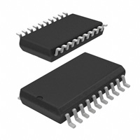
MC100EL14DWG

MC100EL14DWG

  • 厂商:

    ONSEMI(安森美)

  • 封装:

    SOIC-20

  • 描述:

    Clock Fanout Buffer (Distribution), Multiplexer IC 1GHz 20-SOIC (0.295", 7.50mm Width)

  • 详情介绍
  • 数据手册
  • 价格&库存
MC100EL14DWG 数据手册
MC100EL14 5V ECL 1:5 Clock Distribution Chip The MC100EL14 is a low skew 1:5 clock distribution chip designed explicitly for low skew clock distribution applications. The VBB pin, an internally generated voltage supply, is available to this device only. For single-ended input conditions, the unused differential input is connected to VBB as a switching reference voltage. VBB may also rebias AC coupled inputs. When used, decouple VBB and VCC via a 0.01 mF capacitor and limit current sourcing or sinking to 0.5 mA. When not used, VBB should be left open. The EL14 features a multiplexed clock input to allow for the distribution of a lower speed scan or test clock along with the high speed system clock. When LOW (or left open and pulled LOW by the input pulldown resistor) the SEL pin will select the differential clock input. The common enable (EN) is synchronous so that the outputs will only be enabled/disabled when they are already in the LOW state. This avoids any chance of generating a runt clock pulse when the device is enabled/disabled as can happen with an asynchronous control. The internal flip flop is clocked on the falling edge of the input clock, therefore all associated specification limits are referenced to the negative edge of the clock input. http://onsemi.com SOIC−20L DW SUFFIX CASE 751D MARKING DIAGRAM 20 Features • • • • • • 100EL14 AWLYYWWG 50 ps Output-to-Output Skew Synchronous Enable/Disable Multiplexed Clock Input 1 The 100 Series Contains Temperature Compensation PECL Mode Operating Range: VCC = 4.2 V to 5.7 V with VEE = 0 V NECL Mode Operating Range: VCC = 0 V with VEE = −4.2 V to −5.7 V Q Output will Default LOW with Inputs Open or at VEE • • Internal Input Pull−down Resistors on All Inputs, Pull−up Resistors on Inverted Inputs A WL YY WW G = Assembly Location = Wafer Lot = Year = Work Week = Pb−Free Package *For additional marking information, refer to Application Note AND8002/D. ORDERING INFORMATION See detailed ordering and shipping information in the package dimensions section on page 7 of this data sheet. © Semiconductor Components Industries, LLC, 2008 November, 2008 − Rev. 8 1 Publication Order Number: MC100EL14/D MC100EL14 • Pb−Free Packages are Available* *For additional information on our Pb−Free strategy and soldering details, please download the ON Semiconductor Soldering and Mounting Techniques Reference Manual, SOLDERRM/D. http://onsemi.com 2 MC100EL14 VCC 20 EN VCC NC SCLK CLK CLK VBB 19 17 18 16 15 14 13 SEL VEE 12 11 Table 1. PIN DESCRIPTION PIN 10 D Q 1 Q0 2 Q0 3 Q1 4 Q1 5 Q2 6 Q2 7 Q3 8 Q3 9 Q4 FUNCTION CLK, CLK ECL Diff Clock Inputs SCLK ECL Scan Clock Input EN ECL Sync Enable SEL ECL Clock Select Input Q0−4, Q0−4 ECL Diff Clock Outputs 10 VBB Reference Voltage Output Q4 VCC Positive Supply VEE Negative Supply NC No Connect * All VCC pins are tied together on the die. Warning: All VCC and VEE pins must be externally connected to Power Supply to guarantee proper operation. Table 2. FUNCTION TABLE Figure 1. Logic Diagram and Pinout Assignment CLK* SCLK* SEL* EN* Q X X L H X L L H H X L L L L H L H L H L (Note ) L H X X X 1. On next negative transition of CLK or SCLK **Pins will default low when left open. Table 3. ATTRIBUTES Characteristics Value Internal Input Pulldown Resistor 75 kW Internal Input Pullup Resistor 75 kW ESD Protection Human Body Model Machine Model Charge Device Model > 2 kV > 200 V > 4 kV Pb Pb−Free Level 1 Level 3 Moisture Sensitivity (Note 2) Flammability Rating Oxygen Index: 28 to 34 Transistor Count UL 94 V−0 @ 0.125 in 303 Devices Meets or Exceeds JEDEC Spec EIA/JESD78 IC Latchup Test 2. For additional Moisture Sensitivity information, refer to Application Note AND8003/D. http://onsemi.com 3 MC100EL14 Table 4. MAXIMUM RATINGS Symbol Parameter Condition 1 Condition 2 Rating Unit VCC PECL Mode Power Supply VEE = 0 V 8 V VEE NECL Mode Power Supply VCC = 0 V −8 V VI PECL Mode Input Voltage NECL Mode Input Voltage VEE = 0 V VCC = 0 V 6 −6 V V Iout Output Current Continuous Surge 50 100 mA mA IBB VBB Sink/Source ± 0.5 mA TA Operating Temperature Range −40 to +85 °C Tstg Storage Temperature Range −65 to +150 °C qJA Thermal Resistance (Junction−to−Ambient) 0 lfpm 500 lfpm SOIC−20L SOIC−20L 90 60 °C/W °C/W qJC Thermal Resistance (Junction−to−Case) Standard Board SOIC−20L 30 to 35 °C/W Tsol Wave Solder
MC100EL14DWG
物料型号:MC100EL14

器件简介:MC100EL14是一款低偏差1:5时钟分配芯片,专为低偏差时钟分配应用设计。它具有内部产生的电压供应VBB引脚,用于差分输入条件下的参考电压或重新偏置交流耦合输入。

引脚分配:文档提供了详细的引脚功能描述和逻辑图,包括ECL差分时钟输入、ECL扫描时钟输入、ECL同步使能、ECL时钟选择输入、ECL差分时钟输出、参考电压输出、正电源、负电源和无连接引脚。

参数特性:包括内部上拉和下拉电阻值、ESD保护等级、湿度敏感度等级、可燃性等级、晶体管数量、JEDEC规格符合性等。

功能详解:MC100EL14具有50ps的输出到输出偏差、同步使能/禁用、多路复用时钟输入、温度补偿、PECL和NECL模式操作范围、输入默认低电平、所有输入上的内部输入下拉电阻、反相输入上的上拉电阻等特性。

应用信息:文档提供了应用笔记的资源参考,包括ECL时钟分配技术、PECL设计、ECLinPS I/O SPICE建模套件、LVDS与ECL之间的接口、ECL转换器指南等。

封装信息:MC100EL14提供SOIC-20L封装,文档还提供了详细的订购信息和运输信息。

MC100EL14DWG 价格&库存

很抱歉,暂时无法提供与“MC100EL14DWG”相匹配的价格&库存,您可以联系我们找货

免费人工找货