MC100EPT23
3.3�V Dual Differential
LVPECL/LVDS/CML to
LVTTL/LVCMOS Translator
Description
Features
•
•
•
•
•
•
www.onsemi.com
8
8
1
1
SOIC−8 NB
D SUFFIX
CASE
751−07
TSSOP−8
DT SUFFIX
CASE
948R−02
MARKING DIAGRAMS*
8
8
1.5 ns Typical Propagation Delay
Maximum Operating Frequency > 275 MHz
KPT23
ALYW
G
LVPECL/LVDS/CML Inputs, LVTTL/LVCMOS Outputs
1
1
24 mA LVTTL Outputs
Operating Range:
♦ VCC = 3.0 V to 3.6 V with GND = 0 V
These Devices are Pb-Free, Halogen Free and are RoHS Compliant
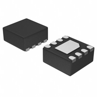
DFN−8
MN SUFFIX
CASE 506AA
A
L
Y
W
M
G
3T M G
G
The MC100EPT23 is a dual differential LVPECL/LVDS/CML to
LVTTL/LVCMOS translator. Because LVPECL (Positive ECL),
LVDS, and positive CML input levels and LVTTL/LVCMOS output
levels are used, only + 3.3 V and ground are required. The small
outline 8-lead SOIC package and the dual gate design of the EPT23
makes it ideal for applications which require the translation of a clock
or data signal.
The EPT23 is available in only the ECL 100K standard. Since there
are no LVPECL outputs or an external VBB reference, the EPT23 does
not require both ECL standard versions. The LVPECL/LVDS inputs
are differential. Therefore, the MC100EPT23 can accept any standard
differential LVPECL/LVDS input referenced from a VCC of + 3.3 V.
KA23
ALYWG
G
1
4
= Assembly Location
= Wafer Lot
= Year
= Work Week
= Date Code
= Pb-Free Package
(Note: Microdot may be in either location)
*For additional marking information, refer to
Application Note AND8002/D.
ORDERING INFORMATION
Device
Package
Shipping†
MC100EPT23DG
SOIC−8 NB
(Pb-Free)
98 Units/Tube
MC100EPT23DR2G
SOIC−8 NB
(Pb-Free)
2500/Tape & Reel
MC100EPT23DTG
TSSOP−8
(Pb-Free)
100 Units/Tube
MC100EPT23DTR2G
TSSOP−8
(Pb-Free)
2500/Tape & Reel
MC100EPT23MNR4G
DFN−8
(Pb-Free)
1000/Tape & Reel
†For information on tape and reel specifications, including part orientation and tape sizes, please refer
to our Tape and Reel Packaging Specifications
Brochure, BRD8011/D.
© Semiconductor Components Industries, LLC, 2016
August, 2016 − Rev. 19
1
Publication Order Number:
MC100EPT23/D
�MC100EPT23
Table 1. PIN DESCRIPTION
D0
D0
1
8
2
7
LVPECL
D1
D1
VCC
Pin
Q0
LVTTL
3
6
4
5
Q1
Function
Q0, Q1
LVTTL/LVCMOS Outputs
D0**, D1**
D0**, D1**
Differential LVPECL/LVDS/CML Inputs
VCC
Positive Supply
GND
Ground
EP
(DFN−8 only) Thermal exposed pad must be
connected to a sufficient thermal conduit.
Electrically connect to the most negative
supply (GND) or leave unconnected, floating
open.
GND
** Pins will default to VCC/2 when left open.
(Top View)
Figure 1. Logic Diagram and 8-Lead Pinout
Table 2. ATTRIBUTES
Characteristics
Value
Internal Input Pulldown Resistor
50 kW
Internal Input Pullup Resistor
50 kW
ESD Protection
Human Body Model
Machine Model
Charged Device Model
> 1500 V
> 100 V
> 2 kV
Moisture Sensitivity, Indefinite Time Out of Drypack (Note 1)
Pb-Free Pkg
SOIC−8 NB
TSSOP−8
DFN−8
Level 1
Level 3
Level 1
Flammability Rating
Oxygen Index: 28 to 34
UL 94 V−0 @ 0.125 in
Transistor Count
91 Devices
Meets or exceeds JEDEC Spec EIA/JESD78 IC Latchup Test
1. For additional information, see Application Note AND8003/D.
Table 3. MAXIMUM RATINGS
Symbol
Parameter
Condition 1
VCC
Power Supply
GND = 0 V
VI
Input Voltage
GND = 0 V
Iout
Output Current
Continuous
Surge
Condition 2
VI ≤ VCC
Rating
Unit
3.8
V
3.8
V
50
100
mA
TA
Operating Temperature Range
−40 to +85
°C
Tstg
Storage Temperature Range
−65 to +150
°C
qJA
Thermal Resistance (Junction-to-Ambient)
0 lfpm
500 lfpm
SOIC−8 NB
190
130
°C/W
qJC
Thermal Resistance (Junction-to-Case)
Standard Board
SOIC−8 NB
41 to 44
°C/W
qJA
Thermal Resistance (Junction-to-Ambient)
0 lfpm
500 lfpm
TSSOP−8
185
140
°C/W
qJC
Thermal Resistance (Junction-to-Case)
Standard Board
TSSOP−8
41 to 44
°C/W
qJA
Thermal Resistance (Junction-to-Ambient)
0 lfpm
500 lfpm
DFN−8
129
84
°C/W
www.onsemi.com
2
�MC100EPT23
Table 3. MAXIMUM RATINGS
Symbol
Parameter
Condition 1
Tsol
Wave Solder (Pb-Free)
很抱歉,暂时无法提供与“MC100EPT23MNR4G”相匹配的价格&库存,您可以联系我们找货
免费人工找货- 国内价格 香港价格
- 1+67.869331+8.78627
- 10+52.4904510+6.79535
- 25+48.6402625+6.29691
- 100+44.52577100+5.76425
- 国内价格
- 1+65.07647
- 10+50.30760
- 25+46.94178
- 50+46.53453