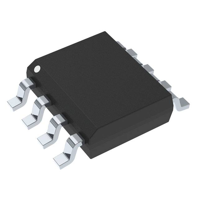
MC100LVEL51
3.3V ECL Differential Clock
D Flip‐Flop
Description
The MC100LVEL51 is a differential clock D flip-flop with reset. The
device is functionally equivalent to the EL51 device, but operates from a
3.3 V supply. With propagation delays and output transition times
essentially equal to the EL51, the LVEL51 is ideally suited for those
applications which require the ultimate in AC performance at 3.3 V VCC.
The reset input is an asynchronous, level triggered signal. Data enters
the master portion of the flip-flop when the clock is LOW and is
transferred to the slave, and thus the outputs, upon a positive transition of
the clock. The differential clock inputs of the LVEL51 allow the device to
be used as a negative edge triggered flip-flop.
The differential input employs clamp circuitry to maintain stability
under open input conditions. When left open, the CLK input will be
pulled down to VEE and the CLK input will be biased at VCC/2.
http://onsemi.com
MARKING
DIAGRAMS*
8
8
1
KVL51
ALYW
G
SOIC−8
D SUFFIX
CASE 751
1
8
8
1
Features
• 475 ps Propagation Delay
• 2.8 GHz Toggle Frequency
• ESD Protection: >4 kV Human Body Model,
TSSOP−8
DT SUFFIX
CASE 948R
1
KV51
ALYWG
G
>200 V Machine Model
4G M G
G
• The 100 Series Contains Temperature Compensation
• PECL Mode Operating Range: VCC = 3.0 V to 3.8 V
with VEE = 0 V
1
• NECL Mode Operating Range: VCC = 0 V
•
•
•
•
•
•
with VEE = −3.0 V to −3.8 V
Internal Input Pulldown Resistors
Meets or Exceeds JEDEC Spec EIA/JESD78 IC Latchup Test
Moisture Sensitivity Level 1
For Additional Information, see Application Note AND8003/D
Flammability Rating: UL 94 V−0 @ 0.125 in,
Oxygen Index: 28 to 34
Transistor Count = 114 devices
Pb−Free Packages are Available
4
DFN8
MN SUFFIX
CASE 506AA
A
L
Y
W
M
G
= Assembly Location
= Wafer Lot
= Year
= Work Week
= Date Code
= Pb−Free Package
(Note: Microdot may be in either location)
*For additional marking information, refer to
Application Note AND8002/D.
ORDERING INFORMATION
See detailed ordering and shipping information in the package
dimensions section on page 6 of this data sheet.
© Semiconductor Components Industries, LLC, 2008
August, 2008 − Rev. 6
1
Publication Order Number:
MC100LVEL51/D
�MC100LVEL51
R
1
D
2
8
VCC
7
Q
R
D
Flip-Flop
CLK
3
6
Q
CLK
4
5
VEE
Figure 1. Logic Diagram and Pinout Assignment
Table 1. PIN DESCRIPTION
Table 2. TRUTH TABLE
PIN
FUNCTION
D
R
CLK
Q
CLK, CLK
ECL Differential Clock Input
ECL Differential Output
ECL D Input
ECL Reset Input
Positive Supp;y
Negative Supply
L
H
X
L
L
H
Z
Z
X
L
H
L
Q, Q
D
R
VCC
VEE
EP
Z = LOW to HIGH Transition
X = Don’t Care
(DFN8 only) Thermal exposed pad must be
connected to a sufficient thermal conduit. Electrically connect to the most negative supply
(GND) or leave unconnected, floating open.
http://onsemi.com
2
�MC100LVEL51
Table 3. MAXIMUM RATINGS
Symbol
Parameter
Condition 1
Rating
Unit
8 to 0
V
−8 to 0
V
6 to 0
−6 to 0
V
V
50
100
mA
mA
Operating Temperature Range
−40 to +85
°C
Storage Temperature Range
−65 to +150
°C
8 SOIC
8 SOIC
190
130
°C/W
°C/W
Standard Board
8 SOIC
41 to 44 ± 5%
°C/W
Thermal Resistance (Junction−to−Ambient)
0 lfpm
500 lfpm
8 TSSOP
8 TSSOP
185
140
°C/W
°C/W
qJC
Thermal Resistance (Junction−to−Case)
Standard Board
8 TSSOP
41 to 44 ± 5%
°C/W
qJA
Thermal Resistance (Junction−to−Ambient)
0 lfpm
500 lfpm
DFN8
DFN8
129
84
°C/W
°C/W
Tsol
Wave Solder
