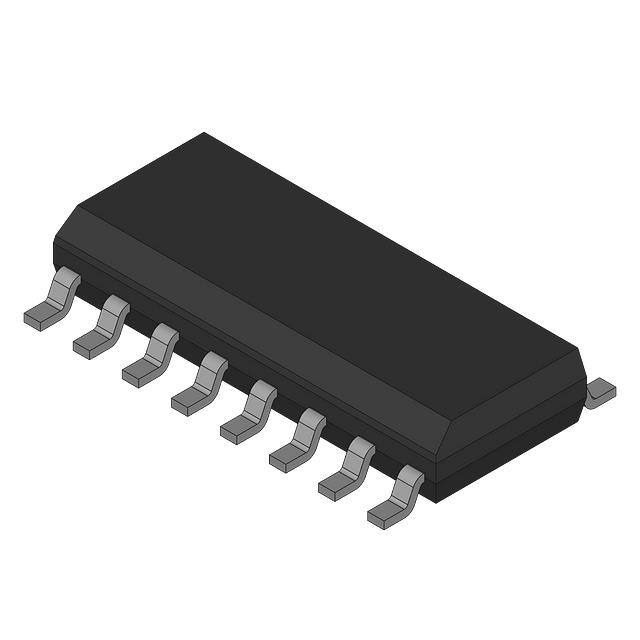
MC100LVEP34
2.5V / 3.3V ECL ÷2, ÷4, ÷8
Clock Generation Chip
The MC100LVEP34 is a low skew ÷2, ÷4, ÷8 clock generation chip
designed explicitly for low skew clock generation applications. The
internal dividers are synchronous to each other, therefore, the common
output edges are all precisely aligned. The VBB pin, an internally
generated voltage supply, is available to this device only. For
single- ended input conditions, the unused differential input is
connected to VBB as a switching reference voltage. VBB may also
rebias AC coupled inputs. When used, decouple VBB and VCC via a
0.01 mF capacitor and limit current sourcing or sinking to 0.5 mA.
When not used, VBB should be left open.
The common enable (EN) is synchronous so that the internal
dividers will only be enabled/disabled when the internal clock is
already in the LOW state. This avoids any chance of generating a runt
clock pulse on the internal clock when the device is enabled/disabled
as can happen with an asynchronous control. An internal runt pulse
could lead to losing synchronization between the internal divider
stages. The internal enable flip-flop is clocked on the falling edge of
the input clock; therefore, all associated specification limits are
referenced to the negative edge of the clock input.
Upon start-up, the internal flip-flops will attain a random state; the
master reset (MR) input allows for the synchronization of the internal
dividers, as well as multiple LVEP34s in a system. Single-ended CLK
input operation is limited to a VCC ≥ 3.0 V in PECL mode, or VEE ≤
-3.0 V in NECL mode.
http://onsemi.com
MARKING
DIAGRAMS*
16
16
SO-16
D SUFFIX
CASE 751B
•�35 ps Output-to-Output Skew
•�Synchronous Enable/Disable
•�Master Reset for Synchronization
•�The 100 Series Contains Temperature Compensation.
•�PECL Mode Operating Range: VCC = 2.375 V to 3.8 V
1
16
100
VP34
ALYWG
G
16
1
TSSOP-16
DT SUFFIX
CASE 948F
A
L, WL
Y
W, WW
G or G
Features
100LVEP34G
AWLYWW
1
1
= Assembly Location
= Wafer Lot
= Year
= Work Week
= Pb-Free Package
(Note: Microdot may be in either location)
*For additional marking information, refer to
Application Note AND8002/D.
with VEE = 0 V
ORDERING INFORMATION
•�NECL Mode Operating Range: VCC = 0 V
See detailed ordering and shipping information in the package
dimensions section on page 8 of this data sheet.
with VEE = -2.375 V to -3.8 V
•�Open Input Default State
•�LVDS Input Compatible
•�Pb-Free Packages are Available
©� Semiconductor Components Industries, LLC, 2007
June, 2007 - Rev. 10
1
Publication Order Number:
MC100LVEP34/D
�MC100LVEP34
Q0
1
Q
Q0
VCC
15
EN
14
NC
13
CLK
12
CLK
÷2
2
R
VCC
16
Q
D
3
R
Q1
4
Q
Q1
÷4
5
R
VCC
6
11
VBB
Q2
7
10
MR
9
VEE
Q
÷8
Q2
8
R
Warning: All VCC and VEE pins must be externally connected
to Power Supply to guarantee proper operation.
Figure 1. 16-Lead Pinout (Top View) and Logic Diagram
Table 1. PIN DESCRIPTION
Pin
Table 2. FUNCTION TABLE
Function
CLK*, CLK**
ECL Diff Clock Inputs
EN*
ECL Sync Enable
MR*
ECL Master Reset
Q0, Q0
ECL Diff ÷2 Outputs
Q1, Q1
ECL Diff ÷4 Outputs
Q2, Q2
ECL Diff ÷8 Outputs
VBB
Reference Voltage Output
VCC
Positive Supply
VEE
Negative Supply
NC
No Connect
CLK
EN
MR
FUNCTION
Z
ZZ
X
L
H
X
L
L
H
Divide
Hold Q0- 3
Reset Q0- 3
Z = Low-to-High Transition
ZZ = High-to-Low Transition
* Pins will default LOW when left open.
**Pins will default to VCC/2 when left open.
http://onsemi.com
2
�MC100LVEP34
Table 3. ATTRIBUTES
Characteristics
Value
Internal Input Pulldown Resistor
75 kW
Internal Input Pullup Resistor
ESD Protection
37.5 kW
Human Body Model
Machine Model
Charged Device Model
> 2 kV
> 200 V
> 2 kV
Moisture Sensitivity, Indefinite Time Out of Drypack (Note 1)
Flammability Rating
Level 1
Oxygen Index: 28 to 34
UL 94 V-O @ 0.125 in
Transistor Count
210 Devices
Meets or exceeds JEDEC Spec EIA/JESD78 IC Latchup Test
1. For additional Moisture Sensitivity information, refer to Application Note AND8003/D.
Table 4. MAXIMUM RATINGS
Symbol
Parameter
Condition 1
Condition 2
Rating
Unit
6
V
-6
V
6
-6
V
V
50
100
mA
mA
± 0.5
mA
-40 to +85
°C
VCC
PECL Mode Power Supply
VEE = 0 V
VEE
NECL Mode Power Supply
VCC = 0 V
VI
PECL Mode Input Voltage
NECL Mode Input Voltage
VEE = 0 V
VCC = 0 V
Iout
Output Current
Continuous
Surge
IBB
VBB Sink/Source
TA
Operating Temperature Range
Tstg
Storage Temperature Range
-65 to +150
°C
qJA
Thermal Resistance (Junction-to-Ambient)
0 lfpm
500 lfpm
SOIC-16
SOIC-16
100
60
°C/W
°C/W
qJC
Thermal Resistance (Junction-to-Case)
Standard Board
SOIC-16
33 to 36
°C/W
qJA
Thermal Resistance (Junction-to-Ambient)
0 lfpm
500 lfpm
TSSOP-16
TSSOP-16
138
108
°C/W
°C/W
qJC
Thermal Resistance (Junction-to-Case)
Standard Board
TSSOP-16
33 to 36
°C/W
Tsol
Wave Solder
很抱歉,暂时无法提供与“MC100LVEP34DR2”相匹配的价格&库存,您可以联系我们找货
免费人工找货