MC10EL35D

MC10EL35D

  • 厂商:

    ONSEMI(安森美)

  • 封装:

    SOIC8_150MIL

  • 描述:

  • 详情介绍
  • 数据手册
  • 价格&库存
MC10EL35D 数据手册
MC10EL35, MC100EL35 5V ECL JK Flip‐Flop Description The MC10EL/100EL35 is a high speed JK flip-flop. The J/K data enters the master portion of the flip-flop when the clock is LOW and is transferred to the slave, and thus the outputs, upon a positive transition of the clock. The reset pin is asynchronous and is activated with a logic HIGH. The 100 Series contains temperature compensation. http://onsemi.com MARKING DIAGRAMS* • 525 ps Propagation Delay • 2.2G Hz Toggle Frequency • ESD Protection: > 1 kV Human Body Model, • • • • 1 > 100 V Machine Model PECL Mode Operating Range: VCC = 4.2 V to 5.7 with VEE = 0 V NECL Mode Operating Range: VCC = 0 V with VEE = −4.2 V to −5.7 V Internal Input Pulldown Resistors on J, K, CLK, and R Meets or Exceeds JEDEC Spec EIA/JESD78 IC Latchup Test Moisture Sensitivity Level 1 For Additional Information, see Application Note AND8003/D Flammability Rating: UL−94 V−0 @ 0.125 in, Oxygen Index 28 to 34 Transistor Count = 81 devices SOIC−8 D SUFFIX CASE 751 8 8 HEL35 ALYW G 1 8 8 1 TSSOP−8 DT SUFFIX CASE 948R KEL35 ALYW G 1 1 8 HL35 ALYWG G 4W M G G • • 8 • • Pb−Free Packages are Available 1 4 1 KL35 ALYWG G 2L M G G Features 1 4 DFN8 MN SUFFIX CASE 506AA H K 4W 2L A = MC10 = MC100 = MC10 = MC100 = Assembly Location L Y W M G = Wafer Lot = Year = Work Week = Date Code = Pb−Free Package (Note: Microdot may be in either location) *For additional marking information, refer to Application Note AND8002/D. ORDERING INFORMATION See detailed ordering and shipping information in the package dimensions section on page 5 of this data sheet. © Semiconductor Components Industries, LLC, 2008 August, 2008 − Rev. 7 1 Publication Order Number: MC10EL35/D MC10EL35, MC100EL35 Table 1. PIN DESCRIPTION J K CLK 1 2 8 J 7 K 3 6 VCC PIN Q Q R R 4 5 VEE FUNCTION J ECL Input K ECL Input R ECL Reset CLK ECL Clock Input Q, Q ECL Data Outputs VCC Positive Supply VEE Negative Supply EP (DFN8 only) Thermal exposed pad must be connected to a sufficient thermal conduit. Electrically connect to the most negative supply (GND) or leave unconnected, floating open. Figure 1. Logic Diagram and Pinout Assignment Table 1. TRUTH TABLE J* K* R* CLK Qn+1 L L H H X L H L H X L L L L H Z Z Z Z X Qn L H Qn L Table 2. MAXIMUM RATINGS Symbol Parameter Condition 1 Condition 2 Rating Unit VCC PECL Mode Power Supply VEE = 0 V 8 V VEE NECL Mode Power Supply VCC = 0 V −8 V VI PECL Mode Input Voltage NECL Mode Input Voltage VEE = 0 V VCC = 0 V 6 −6 V V Iout Output Current Continuous Surge 50 100 mA mA TA Operating Temperature Range −40 to +85 °C Tstg Storage Temperature Range −65 to +150 °C qJA Thermal Resistance (Junction−to−Ambient) 0 lfpm 500 lfpm 8 SOIC 8 SOIC 190 130 °C/W °C/W qJC Thermal Resistance (Junction−to−Case) Standard Board 8 SOIC 41 to 44 °C/W qJA Thermal Resistance (Junction−to−Ambient) 0 lfpm 500 lfpm 8 TSSOP 8 TSSOP 185 140 °C/W °C/W qJC Thermal Resistance (Junction−to−Case) Standard Board 8 TSSOP 41 to 44 ± 5% °C/W qJA Thermal Resistance (Junction−to−Ambient) 0 lfpm 500 lfpm DFN8 DFN8 129 84 °C/W °C/W Tsol Wave Solder
MC10EL35D
物料型号: - 型号:MC10EL35 和 MC100EL35 - 描述:高速JK触发器,MC10EL系列和MC100EL系列

器件简介: - 这些触发器在时钟信号为低电平时接收J/K数据输入,并在时钟信号上升沿时将数据传递到从属部分,从而影响输出。 - 100系列包含温度补偿。

引脚分配: - VCC(8号引脚):正电源 - J(1号引脚):ECL输入 - K(2号引脚):ECL输入 - Q(7号引脚):ECL数据输出 - CLK(3号引脚):ECL时钟输入 - R(4号引脚):ECL复位 - VEE(5号引脚):负电源 - EP(DFN8封装):热暴露垫,必须连接到足够的热传导体

参数特性: - 传播延迟:525ps - 翻转频率:2.2GHz - ESD保护:人体模型>1kV,机器模型>100V - 工作电压范围:PECL模式为4.2V至5.7V,NECL模式为-4.2V至-5.7V - 内部输入下拉电阻:在J、K、CLK和R上 - 
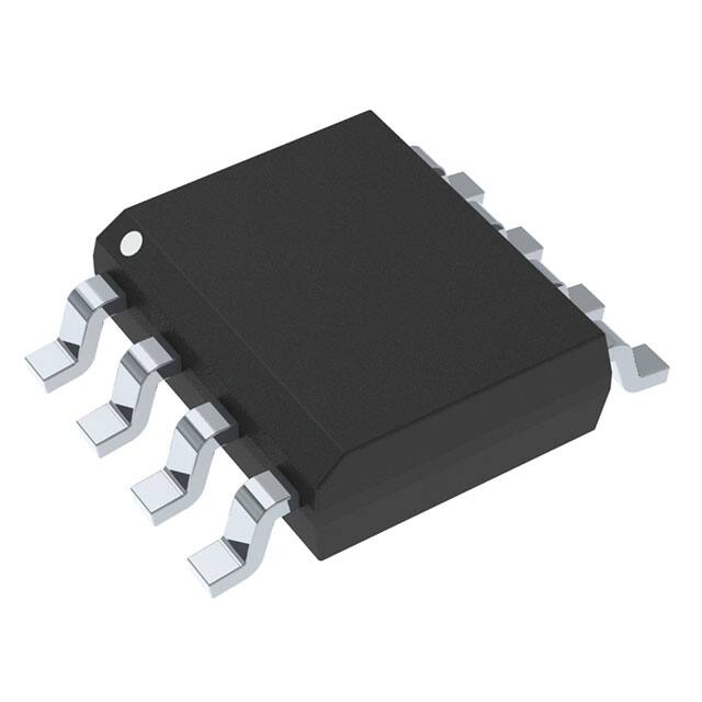
封装类型:SOIC-8、TSSOP-8、DFN8

功能详解: - 该触发器在PECL模式下工作,具有温度补偿功能。 - 具有内部输入下拉电阻,以确保在悬空时输入稳定。 - 符合JEDEC规格,具有防潮等级。

应用信息: - 适用于需要高速和低延迟的应用。 - 100系列由于温度补偿,适用于更广泛的环境。

封装信息: - 提供多种封装选项,包括SOIC-8、TSSOP-8和DFN8。 - 封装信息包括尺寸、引脚间距和标记图。

订购信息: - 提供详细的订购和运输信息,包括封装类型和运输方式。

参考应用文档: - 提供了多个应用文档的参考,如ECL时钟分布技术、PECL设计、ECL I/O SPICE建模套件等。

封装尺寸: - 提供了详细的封装尺寸图表,包括SOIC-8、TSSOP-8和DFN8。
MC10EL35D 价格&库存

很抱歉,暂时无法提供与“MC10EL35D”相匹配的价格&库存,您可以联系我们找货

免费人工找货