MC10ELT21, MC100ELT21
5 V Differential PECL to
TTL Translator
Description
The MC10ELT/100ELT21 is a differential PECL to TTL translator.
Because PECL (Positive ECL) levels are used, only +5 V and ground
are required. The small outline 8-lead package and the single gate of
the ELT21 makes it ideal for those applications where space,
performance and low power are at a premium.
The VBB pin, an internally generated voltage supply, is available to
this device only. For single-ended input conditions, the unused
differential input is connected to VBB as a switching reference voltage.
VBB may also rebias AC coupled inputs. When used, decouple VBB
and VCC via a 0.01 mF capacitor and limit current sourcing or sinking
to 0.5 mA. When not used, VBB should be left open.
The 100 Series contains temperature compensation.
www.onsemi.com
MARKING DIAGRAMS*
8
8
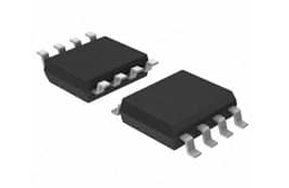
SOIC−8
D SUFFIX
CASE 751
•
•
•
•
•
•
3.5 ns Typical Propagation Delay
24 mA TTL Output
Flow Through Pinouts
Operating Range: VCC = 4.75 V to 5.25 V with GND = 0 V
Q Output Will Default LOW with Inputs Left Open or < 1.3 V
These Devices are Pb−Free, Halogen Free/BFR Free and are RoHS
Compliant
1
TSSOP−8
DT SUFFIX
CASE 948R
H
K
1
= MC10
= MC100
1
KLT21
ALYW
G
1
8
8
Features
8
HLT21
ALYW
G
1
8
HT21
ALYWG
G
A
L
Y
W
G
1
KT21
ALYWG
G
= Assembly Location
= Wafer Lot
= Year
= Work Week
= Pb−Free Package
(Note: Microdot may be in either location)
*For additional marking information, refer to
Application Note AND8002/D.
ORDERING INFORMATION
See detailed ordering and shipping information in the package
dimensions section on page 5 of this data sheet.
© Semiconductor Components Industries, LLC, 2015
August, 2015 − Rev. 13
1
Publication Order Number:
MC10ELT21/D
�MC10ELT21, MC100ELT21
Table 1. PIN DESCRIPTION
NC
D0
1
8
TTL
2
VCC
7
Pin
VBB
3
NC
6
4
TTL Outputs
D0, DO
PECL Differential Outputs
VBB
Reference Voltage Output
VCC
Positive Supply
GND
Ground
NC
No Connect
Q0
PECL
D0
Function
Q0
5
GND
Figure 1. 8−Lead Pinout and Logic Diagram
(Top View)
Table 2. ATTRIBUTES
Characteristics
Value
Internal Input Pulldown Resistor
50 kW
Internal Input Pullup Resistor
ESD Protection
N/A
Human Body Model
> 2 kV
Moisture Sensitivity, Indefinite Time Out of Drypack (Note 1)
Pb−Free Pkg
SOIC−8
TSSOP−8
Flammability Rating
Level 1
Level 3
Oxygen Index: 28 to 34
UL 94 V−0 @ 0.125 in
Transistor Count
81 Devices
Meets or exceeds JEDEC Spec EIA/JESD78 IC Latchup Test
1. For additional information, see Application Note AND8003/D.
Table 3. MAXIMUM RATINGS
Symbol
Parameter
Condition 1
Condition 2
Rating
Unit
7
V
0 to 6
V
± 0.5
mA
−40 to +85
°C
VCC
PECL Power Supply
GND = 0 V
VIN
PECL Input Voltage
GND = 0 V
IBB
VBB Sink/Source
TA
Operating Temperature Range
Tstg
Storage Temperature Range
−65 to +150
°C
qJA
Thermal Resistance (Junction−to−Ambient)
0 lfpm
500 lfpm
SOIC−8
SOIC−8
190
130
°C/W
°C/W
qJC
Thermal Resistance (Junction−to−Case)
Standard Board
SOIC−8
41 to 44
°C/W
qJA
Thermal Resistance (Junction−to−Ambient)
0 lfpm
500 lfpm
TSSOP−8
TSSOP−8
185
140
°C/W
°C/W
Tsol
Wave Solder
很抱歉,暂时无法提供与“MC10ELT21DG”相匹配的价格&库存,您可以联系我们找货
免费人工找货- 国内价格
- 2+23.58214
- 26+22.87400
- 50+22.18668
- 国内价格
- 1+44.32543
- 10+42.69582
- 100+37.80698
- 500+36.82922
