MC10EP90, MC100EP90
Translator, Triple ECL Input to
LVPECL / PECL Output
Description
The MC10/100EP90 is a TRIPLE ECL TO LVPECL/PECL
translator. The device receives differential LVECL or ECL signals and
translates them to differential LVPECL or PECL output signals.
A VBB output is provided for interfacing with Single−Ended LVECL or
ECL signals at the input. If a Single−Ended input is to be used the
VBB output should be connected to the D input. The active signal would
then drive the D input. When used the VBB output should be bypassed
to ground by a 0.01 mF capacitor. The VBB output is designed to act as
the switching reference for the EP90 under Single−Ended input
switching conditions, as a result this pin can only source/sink up to 0.5
mA of current.
To accomplish the level translation the EP90 requires three power
rails. The VCC supply should be connected to the positive supply, and
the VEE connected to the negative supply.
The 100 Series contains temperature compensation.
http://onsemi.com
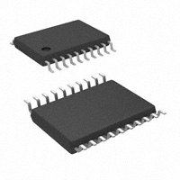
TSSOP−20
DT SUFFIX
CASE 948E
MARKING DIAGRAM*
20
xxxx
EP90
ALYWG
G
Features
• 260 ps Typical Propagation Delay
• Maximum Frequency > 3 GHz Typical
• Voltage Supplies VCC = 3.0 V to 5.5 V, VEE = −3.0 V to −5.5 V,
•
•
•
•
•
•
GND = 0 V
Open Input Default State
Safety Clamp on Inputs
Fully Differential Design
Q Output Will Default LOW with Inputs Open or at VEE
VBB Output
These are Pb−Free Devices*
1
xxxx
= MC10 or 100
A
= Assembly Location
L
= Wafer Lot
Y
= Year
W
= Work Week
G
= Pb−Free Package
(Note: Microdot may be in either location)
*For additional marking information, refer to
Application Note AND8002/D.
ORDERING INFORMATION
See detailed ordering and shipping information in the package
dimensions section on page 7 of this data sheet.
*For additional information on our Pb−Free strategy and soldering details, please
download the ON Semiconductor Soldering and Mounting Techniques
Reference Manual, SOLDERRM/D.
© Semiconductor Components Industries, LLC, 2014
May, 2014 − Rev. 7
1
Publication Order Number:
MC10EP90/D
�MC10EP90, MC100EP90
VCC
Q0
Q0
GND
Q1
Q1
GND
Q2
Q2
VCC
20
19
18
17
16
15
14
13
12
11
Table 1. PIN DESCRIPTION
PIN
FUNCTION
Q(0:2), Q(0:2)
Differential LVPECL or PECL Outputs
D(0:2)*, D(0:2)* Differential LVECL or ECL Inputs
LVPECL/
PECL
LVPECL/
PECL
ECL
LVPECL/
PECL
ECL
ECL
VCC
Positive Supply
GND
Ground
VEE
Negative Supply
VBB
Output Reference Supply
* Pins will default LOW when left open.
Table 2. FUNCTION TABLE
1
2
3
4
5
6
7
8
9
10
VCC
D0
D0
VBB
D1
D1
VBB
D2
D2
VEE
Warning: All VCC, VEE and GND pins must be externally connected to
Power Supply to guarantee proper operation.
Figure 1. TSSOP−20 (Top View) and Logic Diagram
Function
VCC
5V
0V
−5 V
−5V ECL to 3.3V PECL
3.3 V
0V
−5 V
−3.3V ECL to 5V PECL
5V
0V
−3.3 V
−3.3V ECL to 3.3V PECL
3.3 V
0V
−3.3 V
Characteristics
Value
Internal Input Pulldown Resistor
75 kW
Internal Input Pullup Resistor
N/A
Human Body Model
Machine Model
Charged Device Model
Moisture Sensitivity, Indefinite Time Out of Drypack (Note 1)
TSSOP−20
Flammability Rating
Oxygen Index: 28 to 34
Transistor Count
> 2 kV
> 200 V
> 2 kV
Pb Pkg
Pb−Free Pkg
Level 1
Level 1
UL 94 V−0 @ 0.125 in
350 Devices
Meets or exceeds JEDEC Spec EIA/JESD78 IC Latchup Test
1. For additional information, refer to Application Note AND8003/D.
http://onsemi.com
2
VEE
−5V ECL to 5V PECL
Table 3. ATTRIBUTES
ESD Protection
GND
�MC10EP90, MC100EP90
Table 4. MAXIMUM RATINGS
Rating
Unit
VCC
Symbol
PECL Mode Power Supply
Parameter
GND = 0 V
Condition 1
6
V
VEE
NECL Mode Power Supply
GND = 0 V
−6
V
VI
PECL Mode Input Voltage
NECL Mode Input Voltage
GND = 0 V
GND = 0 V
6
−6
V
V
Iout
Output Current
Continuous
Surge
50
100
mA
mA
IBB
VBB Sink/Source
± 0.5
mA
TA
Operating Temperature Range
−40 to +85
°C
Tstg
Storage Temperature Range
−65 to +150
°C
qJA
Thermal Resistance (Junction−to−Ambient)
0 lfpm
500 lfpm
TSSOP−20
TSSOP−20
140
100
°C/W
°C/W
qJC
Thermal Resistance (Junction−to−Case)
Standard Board
TSSOP−20
23 to 41
°C/W
Tsol
Wave Solder
3
240
Within Device Skew
Q, Q
Device to Device Skew (Note 15)
Typ
230
300
370
ps
5.0
20
ps
80
140
0.2
很抱歉,暂时无法提供与“MC10EP90DTG”相匹配的价格&库存,您可以联系我们找货
免费人工找货