MC10H159
Quad 2−Input Multiplexer
(Inverting)
Description
The MC10H159 is a quad 2−input multiplexer with enable. This
MECL 10H™ part is a functional/pinout duplication of the standard
MECL 10K™ family part, with 100% improvement in propagation
delay and no increase in power−supply current.
http://onsemi.com
MARKING DIAGRAMS*
Features
16
• Propagation Delay, 1.5 ns Typical
• Power Dissipation, 218 mW Typical
• Improved Noise Margin 150 mV (Over Operating Voltage and
•
•
•
MC10H159L
AWLYYWW
Temperature Range)
Voltage Compensated
MECL 10K Compatible
Pb−Free Packages are Available*
1
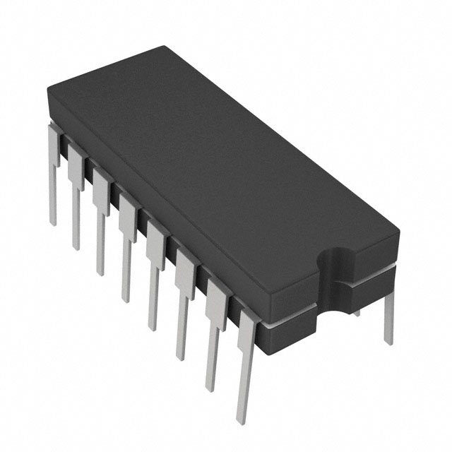
CDIP−16
L SUFFIX
CASE 620A
16
TRUTH TABLE
Enable
Select
D0
D1
Q
L
L
X
L
H
L
L
X
H
L
L
H
L
X
H
L
H
H
X
H
X
X
X
L
L
MC10H159P
AWLYYWWG
16
1
PDIP−16
P SUFFIX
CASE 648
1
10H159
ALYWG
DIP
PIN ASSIGNMENT
SOEIAJ−16
CASE 966
1 20
Q0
1
16
VCC
Q1
2
15
Q2
D11
3
14
Q3
D10
4
13
D20
D01
5
12
D21
D00
6
11
D30
ENABLE
7
10
D31
VEE
8
9
SELECT
PLLC−20
FN SUFFIX
CASE 775
A
WL, L
YY, Y
WW, W
G
Pin assignment is for Dual−in−Line Package.
For PLCC pin assignment, see the Pin Conversion Tables on page 18
of the ON Semiconductor MECL Data Book (DL122/D).
*For additional information on our Pb−Free strategy and soldering details, please
download the ON Semiconductor Soldering and Mounting Techniques
Reference Manual, SOLDERRM/D.
© Semiconductor Components Industries, LLC, 2006
February, 2006 − Rev. 7
10H159G
AWLYYWW
20 1
1
= Assembly Location
= Wafer Lot
= Year
= Work Week
= Pb−Free Package
*For additional marking information, refer to
Application Note AND8002/D.
ORDERING INFORMATION
See detailed ordering and shipping information in the package
dimensions section on page 4 of this data sheet.
Publication Order Number:
MC10H159/D
�MC10H159
Table 1. MAXIMUM RATINGS
Symbol
Rating
Unit
VEE
Power Supply (VCC = 0)
Characteristic
−8.0 to 0
Vdc
VI
Input Voltage (VCC = 0)
0 to VEE
Vdc
Iout
Output Current
50
100
mA
TA
Operating Temperature Range
0 to +75
°C
Tstg
Storage Temperature Range − Plastic
− Ceramic
−55 to +150
−55 to +165
°C
°C
− Continuous
− Surge
Maximum ratings are those values beyond which device damage can occur. Maximum ratings applied to the device are individual stress limit
values (not normal operating conditions) and are not valid simultaneously. If these limits are exceeded, device functional operation is not implied,
damage may occur and reliability may be affected.
Table 2. ELECTRICAL CHARACTERISTICS (VEE = −5.2 V ±5%) (Note 1)
0°
Symbol
IE
IinH
Characteristic
25°
75°
Min
Max
Min
Max
Min
Max
Unit
Power Supply Current
−
58
−
53
−
58
mA
Input Current High
Pin 9
Pins 3−7 and 10−13
−
−
475
515
−
−
295
320
−
−
295
320
0.5
−
0.5
−
0.3
−
mA
−0.735
Vdc
mA
IinL
Input Current Low
VOH
High Output Voltage
−1.02
−0.84
−0.98
−0.81
−0.92
VOL
Low Output Voltage
−1.95
−1.63
−1.95
−1.63
−1.95
−1.60
Vdc
VIH
High Input Voltage
−1.17
−0.84
−1.13
−0.81
−1.07
−0.735
Vdc
VIL
Low Input Voltage
−1.95
−1.48
−1.95
−1.48
−1.95
−1.45
Vdc
1. Each MECL 10H series circuit has been designed to meet the dc specifications shown in the test table, after thermal equilibrium has been
established. The circuit is in a test socket or mounted on a printed circuit board and transverse air flow greater than 500 linear fpm is
maintained. Outputs are terminated through a 50 W resistor to −2.0 V.
Table 3. AC PARAMETERS
0°
Symbol
25°
75°
Min
Max
Min
Max
Min
Max
Propagation Delay
Data
Select
Enable
0.5
1.0
1.0
2.2
3.2
3.2
0.5
1.0
1.0
2.2
3.2
3.2
0.5
1.0
1.0
2.2
3.2
3.2
tr
Rise Time
0.5
2.2
0.5
2.2
0.5
2.2
ns
tf
Fall Time
0.5
2.2
0.5
2.2
0.5
2.2
ns
tpd
Characteristic
Unit
ns
NOTE: Device will meet the specifications after thermal equilibrium has been established when mounted in a test socket or printed circuit
board with maintained transverse airflow greater than 500 lfpm. Electrical parameters are guaranteed only over the declared
operating temperature range. Functional operation of the device exceeding these conditions is not implied. Device specification limit
values are applied individually under normal operating conditions and not valid simultaneously.
http://onsemi.com
2
�MC10H159
APPLICATION INFORMATION
The MC10H159 is a quad two channel multiplexer with
enable. It incorporates common enable and common data
select inputs. The select input determines which data inputs
are enabled. A high (H) level enables data inputs D0 0, D1
0, D2 0, and D3 0. A low (L) level enables data inputs D0
1, D1 1, D2 1, and D3 1. Any change on the data inputs will
be reflected at the outputs while the enable is low. Input
levels are inverted at the output.
LOGIC DIAGRAM
SELECT 9
D0 1 5
1 Q0
D0 0 6
D1 1 3
2 Q1
D1 0 4
ENABLE 7
D2 1 12
15 Q2
D2 0 13
D3 1 10
14 Q3
D3 0 11
VCC PIN 16
VEE PIN 8
http://onsemi.com
3
�MC10H159
ORDERING INFORMATION
Package
Shipping †
MC10H159FN
PLLC−20
46 Units / Rail
MC10H159FNG
PLLC−20
(Pb−Free)
46 Units / Rail
MC10H159FNR2
PLLC−20
500 / Tape & Reel
MC10H159FNR2G
PLLC−20
(Pb−Free)
500 / Tape & Reel
MC10H159L
CDIP−16
25 Unit / Rail
MC10H159M
SOEIAJ−16
50 Unit / Rail
MC10H159MG
SOEIAJ−16
(Pb−Free)
50 Unit / Rail
MC10H159MEL
SOEIAJ−16
2000 / Tape & Reel
MC10H159MELG
SOEIAJ−16
(Pb−Free)
2000 / Tape & Reel
MC10H159P
PDIP−16
25 Unit / Rail
MC10H159PG
PDIP−16
(Pb−Free)
25 Unit / Rail
Device
†For information on tape and reel specifications, including part orientation and tape sizes, please refer to our Tape and Reel Packaging
Specifications Brochure, BRD8011/D.
http://onsemi.com
4
�MC10H159
PACKAGE DIMENSIONS
20 LEAD PLLC
CASE 775−02
ISSUE E
0.007 (0.180) M T L−M
B
Y BRK
−N−
U
N
S
0.007 (0.180) M T L−M
S
S
N
S
D
−L−
−M−
Z
W
20
D
1
V
0.007 (0.180) M T L−M
S
N
S
R
0.007 (0.180) M T L−M
S
N
S
Z
T L−M
S
N
H
J
0.007 (0.180) M T L−M
S
−T−
VIEW S
SEATING
PLANE
F
0.007 (0.180) M T L−M
S
VIEW S
N
S
N
S
K
0.004 (0.100)
G
S
S
K1
E
G1
0.010 (0.250) S T L−M
S
VIEW D−D
A
C
0.010 (0.250)
G1
X
NOTES:
1. DIMENSIONS AND TOLERANCING PER ANSI Y14.5M,
1982.
2. DIMENSIONS IN INCHES.
3. DATUMS −L−, −M−, AND −N− DETERMINED WHERE TOP
OF LEAD SHOULDER EXITS PLASTIC BODY AT MOLD
PARTING LINE.
4. DIMENSION G1, TRUE POSITION TO BE MEASURED AT
DATUM −T−, SEATING PLANE.
5. DIMENSIONS R AND U DO NOT INCLUDE MOLD FLASH.
ALLOWABLE MOLD FLASH IS 0.010 (0.250) PER SIDE.
6. DIMENSIONS IN THE PACKAGE TOP MAY BE SMALLER
THAN THE PACKAGE BOTTOM BY UP TO 0.012 (0.300).
DIMENSIONS R AND U ARE DETERMINED AT THE
OUTERMOST EXTREMES OF THE PLASTIC BODY
EXCLUSIVE OF MOLD FLASH, TIE BAR BURRS, GATE
BURRS AND INTERLEAD FLASH, BUT INCLUDING ANY
MISMATCH BETWEEN THE TOP AND BOTTOM OF THE
PLASTIC BODY.
7. DIMENSION H DOES NOT INCLUDE DAMBAR
PROTRUSION OR INTRUSION. THE DAMBAR
PROTRUSION(S) SHALL NOT CAUSE THE H DIMENSION
TO BE GREATER THAN 0.037 (0.940). THE DAMBAR
INTRUSION(S) SHALL NOT CAUSE THE H DIMENSION TO
BE SMALLER THAN 0.025 (0.635).
http://onsemi.com
5
DIM
A
B
C
E
F
G
H
J
K
R
U
V
W
X
Y
Z
G1
K1
INCHES
MIN
MAX
0.385
0.395
0.385
0.395
0.165
0.180
0.090
0.110
0.013
0.019
0.050 BSC
0.026
0.032
0.020
−−−
0.025
−−−
0.350
0.356
0.350
0.356
0.042
0.048
0.042
0.048
0.042
0.056
−−− 0.020
2_
10 _
0.310
0.330
0.040
−−−
MILLIMETERS
MIN
MAX
9.78
10.03
9.78
10.03
4.20
4.57
2.29
2.79
0.33
0.48
1.27 BSC
0.66
0.81
0.51
−−−
0.64
−−−
8.89
9.04
8.89
9.04
1.07
1.21
1.07
1.21
1.07
1.42
−−−
0.50
2_
10 _
7.88
8.38
1.02
−−−
N
S
�MC10H159
PACKAGE DIMENSIONS
SOEIAJ−16
CASE 966−01
ISSUE A
16
NOTES:
1. DIMENSIONING AND TOLERANCING PER ANSI
Y14.5M, 1982.
2. CONTROLLING DIMENSION: MILLIMETER.
3. DIMENSIONS D AND E DO NOT INCLUDE MOLD
FLASH OR PROTRUSIONS AND ARE MEASURED
AT THE PARTING LINE. MOLD FLASH OR
PROTRUSIONS SHALL NOT EXCEED 0.15 (0.006)
PER SIDE.
4. TERMINAL NUMBERS ARE SHOWN FOR
REFERENCE ONLY.
5. THE LEAD WIDTH DIMENSION (b) DOES NOT
INCLUDE DAMBAR PROTRUSION. ALLOWABLE
DAMBAR PROTRUSION SHALL BE 0.08 (0.003)
TOTAL IN EXCESS OF THE LEAD WIDTH
DIMENSION AT MAXIMUM MATERIAL CONDITION.
DAMBAR CANNOT BE LOCATED ON THE LOWER
RADIUS OR THE FOOT. MINIMUM SPACE
BETWEEN PROTRUSIONS AND ADJACENT LEAD
TO BE 0.46 ( 0.018).
LE
9
Q1
E HE
1
M_
L
8
Z
DETAIL P
D
e
VIEW P
A
DIM
A
A1
b
c
D
E
e
HE
L
LE
M
Q1
Z
A1
b
0.13 (0.005)
c
0.10 (0.004)
M
CDIP−16
L SUFFIX
CERAMIC DIP PACKAGE
CASE 620A−01
ISSUE O
B
A
A
16
9
1
8
B
M
L
16X
0.25 (0.010)
E
F
C
K
T
N
SEATING
PLANE
G
16X
0.25 (0.010)
M
D
T A
http://onsemi.com
6
M
J
T B
MILLIMETERS
MIN
MAX
−−−
2.05
0.05
0.20
0.35
0.50
0.10
0.20
9.90
10.50
5.10
5.45
1.27 BSC
7.40
8.20
0.50
0.85
1.10
1.50
10 _
0_
0.70
0.90
−−−
0.78
INCHES
MIN
MAX
−−− 0.081
0.002
0.008
0.014
0.020
0.007
0.011
0.390
0.413
0.201
0.215
0.050 BSC
0.291
0.323
0.020
0.033
0.043
0.059
10 _
0_
0.028
0.035
−−− 0.031
NOTES:
1. DIMENSIONING AND TOLERANCING PER
ASME Y14.5M, 1994.
2. CONTROLLING DIMENSION: INCH.
3. DIMENSION L TO CENTER OF LEAD WHEN
FORMED PARALLEL.
4. DIMENSION F MAY NARROW TO 0.76 (0.030)
WHERE THE LEAD ENTERS THE CERAMIC
BODY.
5 THIS DRAWING REPLACES OBSOLETE
CASE OUTLINE 620−10.
DIM
A
B
C
D
E
F
G
H
K
L
M
N
INCHES
MIN
MAX
0.750
0.785
0.240
0.295
−−− 0.200
0.015
0.020
0.050 BSC
0.055
0.065
0.100 BSC
0.008
0.015
0.125
0.170
0.300 BSC
0_
15 _
0.020
0.040
MILLIMETERS
MIN
MAX
19.05
19.93
6.10
7.49
−−−
5.08
0.39
0.50
1.27 BSC
1.40
1.65
2.54 BSC
0.21
0.38
3.18
4.31
7.62 BSC
0_
15 _
0.51
1.01
�MC10H159
PACKAGE DIMENSIONS
PDIP−16
P SUFFIX
PLASTIC DIP PACKAGE
CASE 648−08
ISSUE R
−A−
16
9
1
8
B
F
C
NOTES:
1. DIMENSIONING AND TOLERANCING PER ANSI
Y14.5M, 1982.
2. CONTROLLING DIMENSION: INCH.
3. DIMENSION L TO CENTER OF LEADS WHEN
FORMED PARALLEL.
4. DIMENSION B DOES NOT INCLUDE MOLD FLASH.
5. ROUNDED CORNERS OPTIONAL.
L
S
−T−
H
SEATING
PLANE
K
G
D
M
J
16 PL
0.25 (0.010)
M
T A
M
DIM
A
B
C
D
F
G
H
J
K
L
M
S
INCHES
MIN
MAX
0.740
0.770
0.250
0.270
0.145
0.175
0.015
0.021
0.040
0.70
0.100 BSC
0.050 BSC
0.008
0.015
0.110
0.130
0.295
0.305
0_
10 _
0.020
0.040
MILLIMETERS
MIN
MAX
18.80
19.55
6.35
6.85
3.69
4.44
0.39
0.53
1.02
1.77
2.54 BSC
1.27 BSC
0.21
0.38
2.80
3.30
7.50
7.74
0_
10 _
0.51
1.01
MECL 10H and MECL 10K are trademarks of Motorola, Inc.
ON Semiconductor and
are registered trademarks of Semiconductor Components Industries, LLC (SCILLC). SCILLC reserves the right to make changes without further notice
to any products herein. SCILLC makes no warranty, representation or guarantee regarding the suitability of its products for any particular purpose, nor does SCILLC assume any liability
arising out of the application or use of any product or circuit, and specifically disclaims any and all liability, including without limitation special, consequential or incidental damages.
“Typical” parameters which may be provided in SCILLC data sheets and/or specifications can and do vary in different applications and actual performance may vary over time. All
operating parameters, including “Typicals” must be validated for each customer application by customer’s technical experts. SCILLC does not convey any license under its patent rights
nor the rights of others. SCILLC products are not designed, intended, or authorized for use as components in systems intended for surgical implant into the body, or other applications
intended to support or sustain life, or for any other application in which the failure of the SCILLC product could create a situation where personal injury or death may occur. Should
Buyer purchase or use SCILLC products for any such unintended or unauthorized application, Buyer shall indemnify and hold SCILLC and its officers, employees, subsidiaries, affiliates,
and distributors harmless against all claims, costs, damages, and expenses, and reasonable attorney fees arising out of, directly or indirectly, any claim of personal injury or death
associated with such unintended or unauthorized use, even if such claim alleges that SCILLC was negligent regarding the design or manufacture of the part. SCILLC is an Equal
Opportunity/Affirmative Action Employer. This literature is subject to all applicable copyright laws and is not for resale in any manner.
PUBLICATION ORDERING INFORMATION
LITERATURE FULFILLMENT:
N. American Technical Support: 800−282−9855 Toll Free
Literature Distribution Center for ON Semiconductor
USA/Canada
P.O. Box 61312, Phoenix, Arizona 85082−1312 USA
Phone: 480−829−7710 or 800−344−3860 Toll Free USA/Canada Japan: ON Semiconductor, Japan Customer Focus Center
2−9−1 Kamimeguro, Meguro−ku, Tokyo, Japan 153−0051
Fax: 480−829−7709 or 800−344−3867 Toll Free USA/Canada
Phone: 81−3−5773−3850
Email: orderlit@onsemi.com
http://onsemi.com
7
ON Semiconductor Website: http://onsemi.com
Order Literature: http://www.onsemi.com/litorder
For additional information, please contact your
local Sales Representative.
MC10H159/D
�