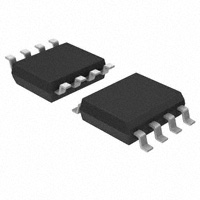
MC10LVEP11DR2G

MC10LVEP11DR2G

  • 厂商:

    ONSEMI(安森美)

  • 封装:

    SOICN-8_4.9X3.9MM

  • 描述:

    IC CLK BUFFER 1:2 3GHZ 8SOIC

  • 详情介绍
  • 数据手册
  • 价格&库存
MC10LVEP11DR2G 数据手册
2.5V/3.3V ECL 1:2 Differential Fanout Buffer MC10LVEP11, MC100LVEP11 Description The MC10/100LVEP11 is a differential 1:2 fanout buffer. The device is pin and functionally equivalent to the EP11 device. With AC performance the same as the EP11 device, the LVEP11 is ideal for applications requiring lower voltage. Single-ended CLK input operation is limited to a VCC w 3.0 V in PECL mode, or VEE v −3.0 V in NECL mode. The 100 Series contains temperature compensation. Features • 240 ps Typical Propagation Delay • Maximum Frequency > 3.0 GHz Typical • PECL Mode Operating Range: 8 8 1 1 SOIC−8 NB D SUFFIX CASE 751−07 TSSOP−8 DT SUFFIX CASE 948R−02 DFN−8 MN SUFFIX CASE 506AA MARKING DIAGRAMS* 8 8 VCC = 2.375 V to 3.8 V with VEE = 0 V HVP11 ALYW G • NECL Mode Operating Range: VCC = 0 V with VEE = −2.375 V to −3.8 V Open Input Default State ♦ • • Q Output Will Default LOW with Inputs Open or at VEE • LVDS Input Compatible • These Devices are Pb-Free, Halogen Free and are RoHS Compliant 1 1 8 8 KVP11 ALYW G 1 1 H K 4K M A HU11 ALYWG G 4K MG G ♦ www.onsemi.com 1 4 KU11 ALYWG G = MC10 L = MC100 Y = MC100 W = Date Code G = Assembly Location = Wafer Lot = Year = Work Week = Pb-Free Package (Note: Microdot may be in either location) *For additional marking information, refer to Application Note AND8002/D. ORDERING INFORMATION Device MC10LVEP11DR2G Package Shipping† 2500 / SOIC−8 NB (Pb-Free) Tape & Reel 100 Units / TSSOP−8 Tube (Pb-Free) 98 Units / SOIC−8 NB MC100LVEP11DG Tube (Pb-Free) 2500 / MC100LVEP11DR2G SOIC−8 NB (Pb-Free) Tape & Reel 100 Units / MC100LVEP11DTG TSSOP−8 Tube (Pb-Free) MC100LVEP11DTR2G TSSOP−8 2500 / (Pb-Free) Tape & Reel MC100LVEP11MNR4G DFN−8 1000 / (Pb-Free) Tape & Reel MC10LVEP11DTG †For information on tape and reel specifications, including part orientation and tape sizes, please refer to our Tape and Reel Packaging Specifications Brochure, BRD8011/D. © Semiconductor Components Industries, LLC, 2016 May, 2021 − Rev. 15 1 Publication Order Number: MC10LVEP11/D MC10LVEP11, MC100LVEP11 Table 1. PIN DESCRIPTION Q0 Q0 Q1 1 2 3 8 7 6 PIN VCC D FUNCTION D*, D** ECL Data Inputs Q0, Q0, Q1, Q1 ECL Data Outputs VCC Positive Supply VEE Negative Supply EP (DFN−8 only) Thermal exposed pad must be connected to a sufficient thermal conduit. Electrically connect to the most negative supply (GND) or leave unconnected, floating open. D *Pins will default to 2/3 VCC when left open. **Pins will default LOW when left open. Q1 4 5 VEE Figure 1. 8-Lead Pinout (Top View) and Logic Diagram Table 2. ATTRIBUTES Characteristics Value Internal Input Pulldown Resistor 75 kW Internal Input Pullup Resistor 37.5 kW ESD Protection Human Body Model Machine Model Charged Device Model > 4 kV > 200 V > 2 kV Moisture Sensitivity, Indefinite Time Out of Drypack (Note 1) Pb-Free Pkg SOIC−8 NB TSSOP−8 DFN−8 Level 1 Level 3 Level 1 Flammability Rating Oxygen Index: 28 to 34 UL 94 V−0 @ 0.125 in Transistor Count 110 Devices Meets or exceeds JEDEC Spec EIA/JESD78 IC Latchup Test 1. For additional information, see Application Note AND8003/D. www.onsemi.com 2 MC10LVEP11, MC100LVEP11 Table 3. MAXIMUM RATINGS Symbol Rating Unit VCC PECL Mode Power Supply Parameter VEE = 0 V Condition 1 Condition 2 6 V VEE NECL Mode Power Supply VCC = 0 V −6 V VI PECL Mode Input Voltage NECL Mode Input Voltage VEE = 0 V VCC = 0 V 6 −6 V Iout Output Current Continuous Surge 50 100 mA TA Operating Temperature Range −40 to +85 °C Tstg Storage Temperature Range −65 to +150 °C qJA Thermal Resistance (Junction-to-Ambient) 0 lfpm 500 lfpm SOIC−8 NB 190 130 °C/W qJC Thermal Resistance (Junction-to-Case) Standard Board SOIC−8 NB 41 to 44 °C/W qJA Thermal Resistance (Junction-to-Ambient) 0 lfpm 500 lfpm TSSOP−8 185 140 °C/W qJC Thermal Resistance (Junction-to-Case) Standard Board TSSOP−8 41 to 44 °C/W qJA Thermal Resistance (Junction-to-Ambient) 0 lfpm 500 lfpm DFN−8 129 84 °C/W qJC Thermal Resistance (Junction-to-Case) (Note 1) DFN−8 35 to 40 °C/W Tsol Wave Solder (Pb-Free)
MC10LVEP11DR2G
物料型号: - MC10LVEP11 - MC100LVEP11

器件简介: MC10/100LVEP11是差分1:2扇出缓冲器。该设备在管脚和功能上与EP11设备等效。LVEP11具有与EP11设备相同的交流性能,非常适合需要较低电压的应用。100系列包含温度补偿。

引脚分配: - D, D:ECL数据输入 - Q0, Q0, Q1, Q1:ECL数据输出 - Vcc:正电源 - VEE:负电源 - EP:(仅限DFN-8)热暴露垫必须连接到足够的热传导体。

参数特性: - 典型传播延迟:240ps - 最大频率:> 3.0 GHz - PECL模式工作范围:VCC = 2.375 V至3.8 V,VEE = 0 V - NECL模式工作范围:VCC = 0 V,VEE = -2.375 V至-3.8 V

功能详解: - 开路输入默认状态:Q输出在输入开路或VEE时默认为低电平。 - LVDS输入兼容。 - 设备无铅、无卤素,符合RoHS标准。

应用信息: 该设备适用于需要低电压和高速性能的应用,例如高速数据传输和通信设备。

封装信息: - SOIC-8 NB (Pb-Free) - TSSOP-8 (Pb-Free) - DFN-8 (Pb-Free)

MC10LVEP11DR2G 价格&库存

很抱歉,暂时无法提供与“MC10LVEP11DR2G”相匹配的价格&库存,您可以联系我们找货

免费人工找货
MC10LVEP11DR2G
  •  国内价格 香港价格
  • 1+71.890711+9.27409
  • 10+55.5696910+7.16864
  • 25+51.5009625+6.64376
  • 100+47.02409100+6.06623
  • 250+45.37065250+5.85293

库存:2450