ON Semiconductor
Is Now
To learn more about onsemi™, please visit our website at
www.onsemi.com
onsemi and and other names, marks, and brands are registered and/or common law trademarks of Semiconductor Components Industries, LLC dba “onsemi” or its affiliates and/or
subsidiaries in the United States and/or other countries. onsemi owns the rights to a number of patents, trademarks, copyrights, trade secrets, and other intellectual property. A listing of onsemi
product/patent coverage may be accessed at www.onsemi.com/site/pdf/Patent-Marking.pdf. onsemi reserves the right to make changes at any time to any products or information herein, without
notice. The information herein is provided “as-is” and onsemi makes no warranty, representation or guarantee regarding the accuracy of the information, product features, availability, functionality,
or suitability of its products for any particular purpose, nor does onsemi assume any liability arising out of the application or use of any product or circuit, and specifically disclaims any and all
liability, including without limitation special, consequential or incidental damages. Buyer is responsible for its products and applications using onsemi products, including compliance with all laws,
regulations and safety requirements or standards, regardless of any support or applications information provided by onsemi. “Typical” parameters which may be provided in onsemi data sheets and/
or specifications can and do vary in different applications and actual performance may vary over time. All operating parameters, including “Typicals” must be validated for each customer application
by customer’s technical experts. onsemi does not convey any license under any of its intellectual property rights nor the rights of others. onsemi products are not designed, intended, or authorized
for use as a critical component in life support systems or any FDA Class 3 medical devices or medical devices with a same or similar classification in a foreign jurisdiction or any devices intended for
implantation in the human body. Should Buyer purchase or use onsemi products for any such unintended or unauthorized application, Buyer shall indemnify and hold onsemi and its officers, employees,
subsidiaries, affiliates, and distributors harmless against all claims, costs, damages, and expenses, and reasonable attorney fees arising out of, directly or indirectly, any claim of personal injury or death
associated with such unintended or unauthorized use, even if such claim alleges that onsemi was negligent regarding the design or manufacture of the part. onsemi is an Equal Opportunity/Affirmative
Action Employer. This literature is subject to all applicable copyright laws and is not for resale in any manner. Other names and brands may be claimed as the property of others.
�MC14067B
Analog Multiplexers /
Demultiplexers
The MC14067 multiplexer/demultiplexer is a digitally controlled
analog switch featuring low ON resistance and very low leakage
current. This device can be used in either digital or analog
applications.
The MC14067 is a 16−channel multiplexer/demultiplexer with an
inhibit and four binary control inputs A, B, C, and D. These control
inputs select 1−of−16 channels by turning ON the appropriate analog
switch (see MC14067 truth table.)
http://onsemi.com
Features
•
•
•
•
•
•
•
•
•
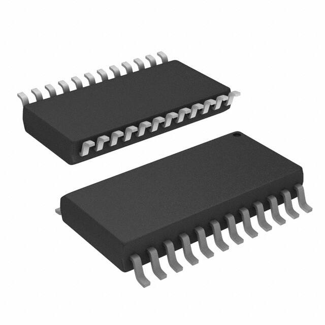
SOIC−24
DW SUFFIX
CASE 751E
Low OFF Leakage Current
Matched Channel Resistance
Low Quiescent Power Consumption
Low Crosstalk Between Channels
Wide Operating Voltage Range: 3 to 18 V
Low Noise
Pin for Pin Replacement for CD4067B
These Devices are Pb−Free and are RoHS Compliant
NLV Prefix for Automotive and Other Applications Requiring
Unique Site and Control Change Requirements; AEC−Q100
Qualified and PPAP Capable
MARKING DIAGRAM
14067B
AWLYYWWG
MAXIMUM RATINGS (Voltages Referenced to VSS)
Symbol
VDD
Parameter
DC Supply Voltage Range
Value
Unit
– 0.5 to + 18.0
V
Vin, Vout
Input or Output Voltage Range
(DC or Transient)
– 0.5 to VDD + 0.5
V
Iin
Input Current (DC or Transient),
per Control Pin
±10
mA
Isw
Switch Through Current
±25
mA
PD
Power Dissipation, per Package
(Note 1)
500
mW
TA
Ambient Temperature Range
– 55 to + 125
_C
Tstg
Storage Temperature Range
– 65 to + 150
_C
TL
Lead Temperature
(8–Second Soldering)
260
_C
A
WL
YY
WW
G
= Assembly Location
= Wafer Lot
= Year
= Work Week
= Pb−Free Package
ORDERING INFORMATION
See detailed ordering and shipping information in the package
dimensions section on page 5 of this data sheet.
Stresses exceeding Maximum Ratings may damage the device. Maximum
Ratings are stress ratings only. Functional operation above the Recommended
Operating Conditions is not implied. Extended exposure to stresses above the
Recommended Operating Conditions may affect device reliability.
1. Temperature Derating:
Plastic “P and D/DW” Packages: − 7.0 mW/_C From 65_C To 125_C
This device contains protection circuitry to guard against damage due to high
static voltages or electric fields. However, precautions must be taken to avoid
applications of any voltage higher than maximum rated voltages to this
high−impedance circuit. For proper operation, Vin and Vout should be constrained
to the range VSS v (Vin or Vout) v VDD.
Unused inputs must always be tied to an appropriate logic voltage level
(e.g., either VSS or VDD). Unused outputs must be left open.
© Semiconductor Components Industries, LLC, 2013
May, 2013 − Rev. 8
1
Publication Order Number:
MC14067B/D
�MC14067B
TRUTH TABLE
Control Inputs
A
B
C
D
Inh
Selected
Channel
X
0
1
0
X
0
0
1
X
0
0
0
X
0
0
0
1
0
0
0
None
X0
X1
X2
1
0
1
0
1
0
0
1
0
1
1
1
0
0
0
0
0
0
0
0
X3
X4
X5
X6
1
0
1
0
1
0
0
1
1
0
0
0
0
1
1
1
0
0
0
0
X7
X8
X9
X10
1
0
1
0
1
1
0
0
1
1
0
1
1
1
1
1
1
1
1
1
0
0
0
0
0
X11
X12
X13
X14
X15
PIN ASSIGNMENT
X
1
24
VDD
X7
2
23
X8
X6
3
22
X9
X5
4
21
X10
X4
5
20
X11
X3
6
19
X12
X2
7
18
X13
X1
8
17
X14
X0
9
16
X15
A
10
15
INHIBIT
B
11
14
C
VSS
12
13
D
16−Channel Analog
Multiplexer/Demultiplexer
CONTROLS
SWITCHES
IN/OUT
FUNCTIONAL DIAGRAM
CONTROL
INPUTS
INHIBIT
A
B
C
D
X
IN/OUT
X0
X1
X2
X3
X4
X5
X6
X7
X8
X9
X10
X11
X12
X13
X14
X15
1-OF-16 DECODER
X
OUT/IN
http://onsemi.com
2
15
10
11
14
13
9
8
7
6
5
4
3
2
23
22
21
20
19
18
17
16
INHIBIT
A
B
C
D
X0
X1
X2
X3
X4
X5
X6
X7
X8
X9
X10
X11
X12
X13
X14
X15
X
1
COMMON
OUT/IN
VDD = PIN 24
VSS = PIN 12
�MC14067B
ELECTRICAL CHARACTERISTICS
− 55°C
Characteristic
Symbol
VDD
Test Conditions
25_C
125_C
Min
Max
Min
Typ (2)
Max
Min
Max
Unit
3.0
18
3.0
−
18
3.0
18
V
−
−
−
5.0
10
20
−
−
−
0.005
0.010
0.015
5.0
10
20
−
−
−
150
300
600
mA
SUPPLY REQUIREMENTS (Voltages Referenced to VSS)
Power Supply Voltage
Range
VDD
−
Quiescent Current Per
Package
IDD
5.0
10
15
Control Inputs: Vin =
VSS or VDD,
Switch I/O: VSS v VI/O v
VDD, and
DVswitch v 500 mV (3)
ID(AV)
5.0
10
15
TA = 25_C only (The
channel component,
(Vin – Vout)/Ron, is
not included.)
Total Supply Current
(Dynamic Plus
Quiescent,
Per Package
mA
(0.07 mA/kHz) f + IDD
(0.20 mA/kHz) f + IDD
(0.36 mA/kHz) f + IDD
Typical
CONTROL INPUTS — INHIBIT, A, B, C, D (Voltages Referenced to VSS)
Low−Level Input Voltage
VIL
5.0
10
15
Ron = per spec,
Ioff = per spec
−
−
−
1.5
3.0
4.0
−
−
−
2.25
4.50
6.75
1.5
3.0
4.0
−
−
−
1.5
3.0
4.0
V
High−Level Input Voltage
VIH
5.0
10
15
Ron = per spec,
Ioff = per spec
3.5
7.0
11
−
−
−
3.5
7.0
11
2.75
5.50
8.25
−
−
−
3.5
7.0
11
−
−
−
V
Input Leakage Current
Iin
15
Vin = 0 or VDD
−
± 0.1
−
± 0.00001
± 0.1
−
1.0
mA
Input Capacitance
Cin
—
−
−
−
5.0
7.5
−
−
pF
SWITCHES IN/OUT AND COMMONS OUT/IN — X, Y (Voltages Referenced to VSS)
Recommended Peak−to−
Peak Voltage Into or
Out of the Switch
VI/O
−
Channel On or Off
0
VDD
0
−
VDD
0
VDD
Vp−p
Recommended Static or
Dynamic Voltage
Across the Switch (3)
(Figure 1)
DVswitch
−
Channel On
0
600
0
−
600
0
300
mV
Output Offset Voltage
VOO
−
Vin = 0 V, No Load
−
−
−
10
−
−
−
mV
ON Resistance
Ron
5.0
10
15
DVswitch v 500 mV (3),
Vin = VIL or VIH
(Control), and Vin
0 to VDD (Switch)
−
−
−
800
400
220
−
−
−
250
120
80
1050
500
280
−
−
−
1300
550
320
W
DRon
5.0
10
15
−
−
−
70
50
45
−
−
−
25
10
10
70
50
45
−
−
−
135
95
65
W
Ioff
15
Vin = VIL or VIH
(Control) Channel to
Channel or Any One
Channel
−
± 100
−
± 0.05
±100
−
± 1000
nA
Capacitance, Switch I/O
CI/O
−
Inhibit = VDD
−
—
—
10
−
−
−
pF
Capacitance, Common O/I
CO/I
−
Inhibit = VDD
(MC14067B)
(MC14097B)
−
−
−
−
−
−
100
60
−
−
−
−
−
−
CI/O
−
−
−
−
−
0.47
−
−
−
DON Resistance
Between
Any Two Channels
in the Same Package
Off−Channel Leakage
Current (Figure 2)
Capacitance, Feedthrough
(Channel Off)
pF
Pins Not Adjacent
Pins Adjacent
pF
2. Data labeled “Typ” is not to be used for design purposes, but is intended as an indication of the IC’s potential performance.
3. For voltage drops across the switch (DVswitch) > 600 mV ( > 300 mV at high temperature), excessive VDD current may be drawn; i.e.
the current out of the switch may contain both VDD and switch input components. The reliability of the device will be unaffected unless the
Maximum Ratings are exceeded. (See first page of this data sheet.)
http://onsemi.com
3
�MC14067B
ELECTRICAL CHARACTERISTICS (CL = 50 pF, TA = 25_C)
Characteristic
Symbol
Propagation Delay Times
Channel Input−to−Channel Output (RL = 200 kW)
MC14067B
VDD – VSS
Vdc
Typ (4)
tPLH, tPHL
(Figure 3)
Propagation Delay Times
Channel Input−to−Channel Output (RL = 1.0 kW)
MC14067B
(Figure 3)
5.0
10
15
35
15
12
90
40
30
ns
5.0
10
15
50
30
20
ns
tPZH, tPZL
Channel Turn−Off Time (RL = 300 kW)
MC14067B
5.0
10
15
240
115
75
600
290
190
ns
(Figure 4)
tPHZ, tPLZ
Channel Turn−Off Time (RL = 10 kW)
MC14067B
5.0
10
15
250
120
75
625
300
190
ns
(Figure 4)
5.0
10
15
Any Pair of Address Inputs to Output
MC14067B
625
450
350
tPLH, tPHL
Second Harmonic Distortion
(RL = 10 kW, f = 1 kHz, Vin = 5 Vp−p)
−
ns
5.0
10
15
280
115
85
700
290
215
10
0.3
−
BW
MC14067B
Off Channel Feedthrough Attenuation
[RL = 50 W, Vin = 1/2 (VDD−VSS) p−p(sine−wave)]
fin = 20 MHz – MC14067B
Channel Separation
[RL = 1 kW, Vin = 1/2 (VDD−VSS) p−p (sine−wave)]
Unit
ns
tPLH, tPHL
Control Input−to−Channel Output
Channel Turn−On Time (RL = 10 kW)
MC14067B
ON Channel Bandwidth
[RL = 50 W, Vin = 1/2 (VDD – VSS) p−p(sine−wave)]
20 Log10 (Vout/Vin) = − 3 dB
Max
fin = 20 MHz
MHz
(Figure 5)
10
15
−
−
10
– 40
−
dB
10
– 40
−
dB
10
30
−
mV
(Figure 5)
−
Crosstalk, Control Inputs−to−Common O/I
(R1 = 1 kW, RL = 10 kW,
Control tr = tf = 20 ns, Inhibit = VSS)
(Figure 6)
−
(Figure 7)
4. Data labelled “Typ” is not to be used for design purposes but is intended as an indication of the IC’s potential performance.
http://onsemi.com
4
%
�MC14067B
ORDERING INFORMATION
Device
MC14067BDWG
NLV14067BDWG*
MC14067BDWR2G
NLV14067BDWR2G*
Package
Shipping†
SOIC−24
(Pb−Free)
30 Units / Rail
SOIC−24
(Pb−Free)
1000 Units / Tape & Reel
†For information on tape and reel specifications, including part orientation and tape sizes, please refer to our Tape and Reel Packaging
Specifications Brochure, BRD8011/D.
*NLV Prefix for Automotive and Other Applications Requiring Unique Site and Control Change Requirements; AEC−Q100 Qualified and PPAP
Capable.
OFF CHANNEL UNDER TEST
VDD
ON SWITCH
A
CONTROL
SECTION
OF IC
CONTROL
SECTION
OF IC
VSS
OTHER
CHANNEL(S)
LOAD
VSS
VDD
V
SOURCE
VSS
VDD
Figure 2. Off Channel Leakage
Figure 1. DV Across Switch
VC
PULSE
GENERATOR
VDD
A
B
C
D
Vout
RL
CL = 50 pF
VDD VSS
20 ns
20 ns
90%
50%
tPLH
VC
VX
VSS VDD
20 ns
90%
50%
10%
VDD
10%
tPHL
Vout
VSS
90%
50%
tPZH, tPZL
Vout
CL = 50 pF
RL
Vin
Vin
Vin
Vout
INH
INH
20 ns
A
B
C
D
50%
Vout
Figure 3. Propagation Delay Test Circuit
and Waveforms Vin to Vout
tPHZ, tPLZ
50%
10%
Figure 4. Turn−On and Delay Turn−Off
Test Circuit and Waveforms
http://onsemi.com
5
Vin = VDD
VX = VSS
Vin = VSS
VX = VDD
�MC14067B
VDD
A, B, and C inputs used to turn ON or OFF
the switch under test.
A
B
C
D
RL
A
B
C
D
ON
INH
OFF
Vout
Vout
INH
RL
RL
CL = 50 pF
CL = 50 pF
Vin
Vin
Figure 5. Bandwidth and Off−Channel
Feedthrough Attenuation
Figure 6. Channel Separation
(Adjacent Channels Used for Setup)
A
B
C
D
VC
Vout
RL
INH
CL = 50 pF
R1
Figure 7. Crosstalk, Control to Common O/I
VA
VB
A
B
C
D
INH
CL
VDD
KEITHLEY 160
DIGITAL
MULTIMETER
10 k
VDD
1 kW
RANGE
X-Y
PLOTTER
VDD
Vout
VA
50%
VB
50%
tPHL
VSS
Vout
Figure 8. Channel Resistance (RON) Test Circuit
tPLH
50%
Figure 9. Propagation Delay, Any Pair of
Address Inputs to Output
http://onsemi.com
6
�MC14067B
350
300
300
250
200
150
TA = 125°C
100
25°C
-�55°C
50
0
-�10
R ON , “ON” RESISTANCE (OHMS)
R ON , “ON” RESISTANCE (OHMS)
350
-�8.0 -�6.0 -�4.0 -�2.0
0
0.2
4.0
6.0
8.0
250
200
150
25°C
-�55°C
50
-�8.0 -�6.0 -�4.0 -�2.0
0
0.2
4.0
6.0
Vin, INPUT VOLTAGE (VOLTS)
Vin, INPUT VOLTAGE (VOLTS)
Figure 10. VDD = 7.5 V, VSS = − 7.5 V
Figure 11. VDD = 5.0 V, VSS = − 5.0 V
700
350
600
300
500
400
300
TA = 125°C
200
25°C
100
0
-�10
TA = 125°C
100
0
-�10
10
RON , “ON” RESISTANCE (OHMS)
R ON , “ON” RESISTANCE (OHMS)
TYPICAL RESISTANCE CHARACTERISTICS
-�55°C
-�8.0 -�6.0 -�4.0 -�2.0
0
0.2
4.0
6.0
8.0
VDD = 2.5 V
200
150
5.0 V
100
7.5 V
50
-�8.0 -�6.0 -�4.0 -�2.0
0
0.2
4.0
6.0
8.0
Vin, INPUT VOLTAGE (VOLTS)
Vin, INPUT VOLTAGE (VOLTS)
Figure 12. VDD = 2.5 V, VSS = − 2.5 V
Figure 13. Comparison at 25°C, VDD = −�VSS
http://onsemi.com
7
10
TA = 25°C
250
0
-�10
10
8.0
10
�MC14067B
APPLICATIONS INFORMATION
Figure A illustrates use of the Analog Multiplexer /
Demultiplexer. The 0−to−5 V Digital Control signal is used
to directly control a 5 Vp−p analog signal.
The digital control logic levels are determined by VDD
and VSS. The VDD voltage is the logic high voltage; the VSS
voltage is logic low. For the example. VDD = + 5 V = logic
high at the control inputs; VSS = GND = 0 V = logic low.
The maximum analog signal level is determined by VDD
and VSS. The analog voltage must swing neither higher than
VDD nor lower than VSS. The example shows a 5 Vp−p
signal which allows no margin at either peak. If voltage
transients above VDD and/or below VSS are anticipated on
the analog channels, external diodes (Dx) are recommended
as shown in Figure B. These diodes should be small signal
types able to absorb the maximum anticipated current surges
during clipping.
The absolute maximum potential difference between VDD
and VSS is 18.0 volts. Most parameters are specified up to
15 V which is the recommended maximum difference
between VDD and VSS.
+5 V
VDD
VSS
+�5.0 V
5 Vp-p
SWITCH
I/O
ANALOG SIGNAL
COMMON
O/I
+5 V
5 Vp-p
ANALOG SIGNAL
GND
MC14067B
EXTERNAL
CMOS
DIGITAL
CIRCUITRY
+ 2.5 V
0-TO-5 V DIGITAL
CONTROL SIGNALS
Figure A. Application Example
VDD
VDD
DX
DX
SWITCH
I/O
COMMON
O/I
DX
DX
VSS
VSS
Figure B. External Germanium or Schottky Clipping Diodes
http://onsemi.com
8
�MC14067B
PACKAGE DIMENSIONS
SOIC−24 WB
CASE 751E−04
ISSUE F
D
24
E
H
A
B
0.25 C
NOTES:
1. DIMENSIONING AND TOLERANCING PER ASME
Y14.5M, 1994.
2. CONTROLLING DIMENSION: MILLIMETERS.
3. DIMENSIONS b AND c APPLY TO THE FLAT SECTION OF THE LEAD AND ARE MEASURED
BETWEEN 0.10 AND 0.25 FROM THE LEAD TIP.
4. DIMENSIONS D AND E1 DO NOT INCLUDE MOLD
FLASH, PROTRUSIONS OR GATE BURRS. MOLD
FLASH, PROTRUSIONS OR GATE BURRS SHALL
NOT EXCEED 0.15 mm PER SIDE. INTERLEAD
FLASH OR PROTRUSION SHALL NOT EXCEED
0.25 PER SIDE. DIMENSIONS D AND E1 ARE
DETERMINED AT DATUM H.
5. A1 IS DEFINED AS THE VERTICAL DISTANCE
FROM THE SEATING PLANE TO THE LOWEST
POINT ON THE PACKAGE BODY.
13
E1
1
L
12
C
DETAIL A
24X b
PIN 1
INDICATOR
0.25
TOP VIEW
M
C A
S
B
S
h
x 45 _
A
A1
NOTE 5
e
DIM
A
A1
b
c
D
E
E1
e
h
L
M
NOTE 3
C
c
SEATING
PLANE
NOTE 3
M
DETAIL A
END VIEW
SIDE VIEW
MILLIMETERS
MIN
MAX
2.35
2.65
0.13
0.29
0.35
0.49
0.23
0.32
15.25
15.54
10.30 BSC
7.40
7.60
1.27 BSC
0.25
0.75
0.41
0.90
0_
8_
RECOMMENDED
SOLDERING FOOTPRINT*
24X
24X
1.62
0.52
11.00
1
1.27
PITCH
DIMENSIONS: MILLIMETERS
*For additional information on our Pb−Free strategy and soldering
details, please download the ON Semiconductor Soldering and
Mounting Techniques Reference Manual, SOLDERRM/D.
ON Semiconductor and
are registered trademarks of Semiconductor Components Industries, LLC (SCILLC). SCILLC owns the rights to a number of patents, trademarks,
copyrights, trade secrets, and other intellectual property. A listing of SCILLC’s product/patent coverage may be accessed at www.onsemi.com/site/pdf/Patent−Marking.pdf. SCILLC
reserves the right to make changes without further notice to any products herein. SCILLC makes no warranty, representation or guarantee regarding the suitability of its products for any
particular purpose, nor does SCILLC assume any liability arising out of the application or use of any product or circuit, and specifically disclaims any and all liability, including without
limitation special, consequential or incidental damages. “Typical” parameters which may be provided in SCILLC data sheets and/or specifications can and do vary in different applications
and actual performance may vary over time. All operating parameters, including “Typicals” must be validated for each customer application by customer’s technical experts. SCILLC
does not convey any license under its patent rights nor the rights of others. SCILLC products are not designed, intended, or authorized for use as components in systems intended for
surgical implant into the body, or other applications intended to support or sustain life, or for any other application in which the failure of the SCILLC product could create a situation where
personal injury or death may occur. Should Buyer purchase or use SCILLC products for any such unintended or unauthorized application, Buyer shall indemnify and hold SCILLC and
its officers, employees, subsidiaries, affiliates, and distributors harmless against all claims, costs, damages, and expenses, and reasonable attorney fees arising out of, directly or indirectly,
any claim of personal injury or death associated with such unintended or unauthorized use, even if such claim alleges that SCILLC was negligent regarding the design or manufacture
of the part. SCILLC is an Equal Opportunity/Affirmative Action Employer. This literature is subject to all applicable copyright laws and is not for resale in any manner.
PUBLICATION ORDERING INFORMATION
LITERATURE FULFILLMENT:
Literature Distribution Center for ON Semiconductor
P.O. Box 5163, Denver, Colorado 80217 USA
Phone: 303−675−2175 or 800−344−3860 Toll Free USA/Canada
Fax: 303−675−2176 or 800−344−3867 Toll Free USA/Canada
Email: orderlit@onsemi.com
N. American Technical Support: 800−282−9855 Toll Free
USA/Canada
Europe, Middle East and Africa Technical Support:
Phone: 421 33 790 2910
Japan Customer Focus Center
Phone: 81−3−5817−1050
http://onsemi.com
9
ON Semiconductor Website: www.onsemi.com
Order Literature: http://www.onsemi.com/orderlit
For additional information, please contact your local
Sales Representative
MC14067B/D
�