ON Semiconductor
Is Now
To learn more about onsemi™, please visit our website at
www.onsemi.com
onsemi and and other names, marks, and brands are registered and/or common law trademarks of Semiconductor Components Industries, LLC dba “onsemi” or its affiliates and/or
subsidiaries in the United States and/or other countries. onsemi owns the rights to a number of patents, trademarks, copyrights, trade secrets, and other intellectual property. A listing of onsemi
product/patent coverage may be accessed at www.onsemi.com/site/pdf/Patent-Marking.pdf. onsemi reserves the right to make changes at any time to any products or information herein, without
notice. The information herein is provided “as-is” and onsemi makes no warranty, representation or guarantee regarding the accuracy of the information, product features, availability, functionality,
or suitability of its products for any particular purpose, nor does onsemi assume any liability arising out of the application or use of any product or circuit, and specifically disclaims any and all
liability, including without limitation special, consequential or incidental damages. Buyer is responsible for its products and applications using onsemi products, including compliance with all laws,
regulations and safety requirements or standards, regardless of any support or applications information provided by onsemi. “Typical” parameters which may be provided in onsemi data sheets and/
or specifications can and do vary in different applications and actual performance may vary over time. All operating parameters, including “Typicals” must be validated for each customer application
by customer’s technical experts. onsemi does not convey any license under any of its intellectual property rights nor the rights of others. onsemi products are not designed, intended, or authorized
for use as a critical component in life support systems or any FDA Class 3 medical devices or medical devices with a same or similar classification in a foreign jurisdiction or any devices intended for
implantation in the human body. Should Buyer purchase or use onsemi products for any such unintended or unauthorized application, Buyer shall indemnify and hold onsemi and its officers, employees,
subsidiaries, affiliates, and distributors harmless against all claims, costs, damages, and expenses, and reasonable attorney fees arising out of, directly or indirectly, any claim of personal injury or death
associated with such unintended or unauthorized use, even if such claim alleges that onsemi was negligent regarding the design or manufacture of the part. onsemi is an Equal Opportunity/Affirmative
Action Employer. This literature is subject to all applicable copyright laws and is not for resale in any manner. Other names and brands may be claimed as the property of others.
�MC14541B
Programmable Timer
The MC14541B programmable timer consists of a 16−stage binary
counter, an integrated oscillator for use with an external capacitor and
two resistors, an automatic power−on reset circuit, and output control
logic.
Timing is initialized by turning on power, whereupon the power−on
reset is enabled and initializes the counter, within the specified VDD
range. With the power already on, an external reset pulse can be
applied. Upon release of the initial reset command, the oscillator will
oscillate with a frequency determined by the external RC network. The
16−stage counter divides the oscillator frequency (fosc) with the nth
stage frequency being fosc/2n.
Features
www.onsemi.com
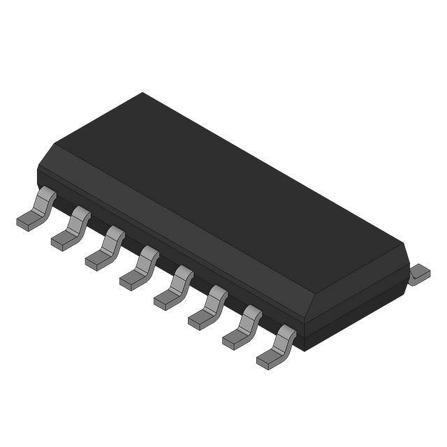
SOIC−14
D SUFFIX
CASE 751A
• Available Outputs 28, 210, 213 or 216
• Increments on Positive Edge Clock Transitions
• Built−in Low Power RC Oscillator (±2% accuracy over temperature
•
•
•
•
•
•
•
•
•
•
range and ±20% supply and ±3% over processing at < 10 kHz)
Oscillator May Be Bypassed if External Clock Is Available
(Apply external clock to Pin 3)
External Master Reset Totally Independent of Automatic Reset
Operation
Operates as 2n Frequency Divider or Single Transition Timer
Q/Q Select Provides Output Logic Level Flexibility
Reset (auto or master) Disables Oscillator During Resetting to
Provide No Active Power Dissipation
Clock Conditioning Circuit Permits Operation with Very Slow Clock
Rise and Fall Times
Automatic Reset Initializes All Counters On Power Up
Supply Voltage Range = 3.0 Vdc to 18 Vdc with Auto Reset
Supply Voltage Range = Disabled (Pin 5 = VDD)
Supply Voltage Range = 8.5 Vdc to 18 Vdc with Auto Reset
Supply Voltage Range = Enabled (Pin 5 = VSS)
NLV Prefix for Automotive and Other Applications Requiring
Unique Site and Control Change Requirements; AEC−Q100
Qualified and PPAP Capable
These Devices are Pb−Free and are RoHS Compliant
TSSOP−14
DT SUFFIX
CASE 948G
SOEIAJ−14
F SUFFIX
CASE 965
PIN ASSIGNMENT
Rtc
1
14
VDD
Ctc
2
13
B
RS
3
12
A
NC
4
11
NC
MODE
AR
5
10
MR
6
9
Q/Q SEL
VSS
7
8
Q
NC = NO CONNECTION
MARKING DIAGRAMS
14
14
14541BG
AWLYWW
MC14541B
ALYWG
1
1
SOIC−14
SOEIAJ−14
14
14
541B
ALYWG
G
1
TSSOP−14
A
WL, L
YY, Y
WW, W
G or G
= Assembly Location
= Wafer Lot
= Year
= Work Week
= Pb−Free Package
(Note: Microdot may be in either location)
ORDERING INFORMATION
See detailed ordering and shipping information in the package
dimensions section on page 2 of this data sheet.
© Semiconductor Components Industries, LLC, 2014
December, 2018 − Rev. 15
1
Publication Order Number:
MC14541B/D
�MC14541B
MAXIMUM RATINGS (Voltages Referenced to VSS)
Parameter
Symbol
VDD
Vin, Vout
DC Supply Voltage Range
Input or Output Voltage Range, (DC or Transient)
Value
Unit
−0.5 to +18.0
V
−0.5 to VDD + 0.5
V
Iin
Input Current (DC or Transient)
±10 (per Pin)
mA
Iout
Output Current (DC or Transient)
±45 (per Pin)
mA
PD
Power Dissipation, per Package (Note 1)
500
mW
TA
Ambient Temperature Range
−55 to +125
°C
Tstg
Storage Temperature Range
−65 to +150
°C
TL
Lead Temperature, (8−Second Soldering)
260
°C
Stresses exceeding those listed in the Maximum Ratings table may damage the device. If any of these limits are exceeded, device functionality
should not be assumed, damage may occur and reliability may be affected.
1. Temperature Derating: “D/DW” Packages: –7.0 mW/_C From 65_C To 125_C
ORDERING INFORMATION
Package
Shipping†
MC14541BDG
SOIC−14
(Pb−Free)
55 Units / Rail
NLV14541BDG*
SOIC−14
(Pb−Free)
55 Units / Rail
MC14541BDR2G
SOIC−14
(Pb−Free)
2500 / Tape & Reel
NLV14541BDR2G*
SOIC−14
(Pb−Free)
2500 / Tape & Reel
MC14541BDTR2G
TSSOP−14
(Pb−Free)
2500 / Tape & Reel
NLV14541BDTR2G*
TSSOP−14
(Pb−Free)
2500 / Tape & Reel
MC14541BFELG
SOEIAJ−14
(Pb−Free)
2000 / Tape & Reel
Device
†For information on tape and reel specifications, including part orientation and tape sizes, please refer to our Tape and Reel Packaging
Specifications Brochure, BRD8011/D.
*NLV Prefix for Automotive and Other Applications Requiring Unique Site and Control Change Requirements; AEC−Q100 Qualified and PPAP
Capable.
www.onsemi.com
2
�MC14541B
ELECTRICAL CHARACTERISTICS (Voltages Referenced to VSS)
Symbol
Characteristic
Output Voltage
Vin = VDD or 0
VDD
Vdc
− 55_C
25_C
125_C
Min
Max
Min
Typ
(Note 2)
Max
Min
Max
Unit
“0” Level
VOL
5.0
10
15
−
−
−
0.05
0.05
0.05
−
−
−
0
0
0
0.05
0.05
0.05
−
−
−
0.05
0.05
0.05
Vdc
“1” Level
VOH
5.0
10
15
4.95
9.95
14.95
−
−
−
4.95
9.95
14.95
5.0
10
15
−
−
−
4.95
9.95
14.95
−
−
−
Vdc
“0” Level
VIL
5.0
10
15
−
−
−
1.5
3.0
4.0
−
−
−
2.25
4.50
6.75
1.5
3.0
4.0
−
−
−
1.5
3.0
4.0
5.0
10
15
3.5
7.0
11
−
−
−
3.5
7.0
11
2.75
5.50
8.25
−
−
−
3.5
7.0
11
−
−
−
5.0
10
15
–4.19
–7.96
–16.3
−
−
−
–3.38
–6.42
–13.2
–6.75
–12.83
–26.33
−
−
−
–2.37
–4.49
−9.24
−
−
−
IOL
5.0
10
15
1.93
4.96
19.3
−
−
−
1.56
4.0
15.6
3.12
8.0
31.2
−
−
−
1.09
2.8
10.9
−
−
−
mAdc
Input Current
Iin
15
−
±0.1
−
±0.00001
±0.1
−
±1.0
mAdc
Input Capacitance
(Vin = 0)
Cin
−
−
−
−
5.0
7.5
−
−
pF
Quiescent Current
(Pin 5 is High)
Auto Reset Disabled
IDD
5.0
10
15
−
−
−
5.0
10
20
−
−
−
0.005
0.010
0.015
5.0
10
20
−
−
−
150
300
600
mAdc
Auto Reset Quiescent Current
(Pin 5 is low)
IDDR
10
15
−
−
250
500
−
−
30
82
250
500
−
−
1500
2000
mAdc
Supply Current (Notes 3 & 4)
(Dynamic plus Quiescent)
ID
5.0
10
15
Vin = 0 or VDD
Input Voltage
(VO = 4.5 or 0.5 Vdc)
(VO = 9.0 or 1.0 Vdc)
(VO = 13.5 or 1.5 Vdc)
“1” Level
(VO = 0.5 or 4.5 Vdc)
(VO = 1.0 or 9.0 Vdc)
(VO = 1.5 or 13.5 Vdc)
Output Drive Current
(VOH = 2.5 Vdc)
(VOH = 9.5 Vdc)
(VOH = 13.5 Vdc)
Source
(VOL = 0.4 Vdc)
(VOL = 0.5 Vdc)
(VOL = 1.5 Vdc)
Sink
VIH
IOH
Vdc
Vdc
mAdc
ID = (0.4 mA/kHz) f + IDD
ID = (0.8 mA/kHz) f + IDD
ID = (1.2 mA/kHz) f + IDD
mAdc
Product parametric performance is indicated in the Electrical Characteristics for the listed test conditions, unless otherwise noted. Product
performance may not be indicated by the Electrical Characteristics if operated under different conditions.
2. Data labelled “Typ” is not to be used for design purposes but is intended as an indication of the IC’s potential performance.
3. The formulas given are for the typical characteristics only at 25_C.
4. When using the on chip oscillator the total supply current (in mAdc) becomes: IT = ID + 2 Ctc VDD f x 10–3 where ID is in mA, Ctc is in pF,
VDD in Volts DC, and f in kHz. (see Fig. 3) Dissipation during power−on with automatic reset enabled is typically 50 mA @ VDD = 10 Vdc.
www.onsemi.com
3
�MC14541B
SWITCHING CHARACTERISTICS (Note 5) (CL = 50 pF, TA = 25_C)
Symbol
Characteristic
VDD
Min
Typ
(Note 6)
Max
5.0
10
15
−
−
−
100
50
40
200
100
80
5.0
10
15
−
−
−
3.5
1.25
0.9
10.5
3.8
2.9
5.0
10
15
−
−
−
6.0
3.5
2.5
18
10
7.5
tWH(cl)
5.0
10
15
900
300
225
300
100
85
−
−
−
ns
fcl
5.0
10
15
−
−
−
1.5
4.0
6.0
0.75
2.0
3.0
MHz
tWH(R)
5.0
10
15
900
300
225
300
100
85
−
−
−
ns
trem
5.0
10
15
420
200
200
210
100
100
−
−
−
ns
Output Rise and Fall Time
tTLH, tTHL = (1.5 ns/pF) CL + 25 ns
tTLH, tTHL = (0.75 ns/pF) CL + 12.5 ns
tTLH, tTHL = (0.55 ns/pF) CL + 9.5 ns
tTLH,
tTHL
Propagation Delay, Clock to Q (28 Output)
tPLH, tPHL = (1.7 ns/pF) CL + 3415 ns
tPLH, tPHL = (0.66 ns/pF) CL + 1217 ns
tPLH, tPHL = (0.5 ns/pF) CL + 875 ns
tPLH
tPHL
Propagation Delay, Clock to Q (216 Output)
tPHL, tPLH = (1.7 ns/pF) CL + 5915 ns
tPHL, tPLH = (0.66 ns/pF) CL + 3467 ns
tPHL, tPLH = (0.5 ns/pF) CL + 2475 ns
tPHL
tPLH
Clock Pulse Width
Clock Pulse Frequency (50% Duty Cycle)
MR Pulse Width
Master Reset Removal Time
Unit
ns
ms
ms
5. The formulas given are for the typical characteristics only at 25_C.
6. Data labelled “Typ” is not to be used for design purposes but is intended as an indication of the IC’s potential performance.
VDD
PULSE
GENERATOR
VDD
PULSE
GENERATOR
RS
AR
Q/Q SELECT
MODE
RS
AR
Q/Q SELECT
MODE
A
B
MR
Q
A
B
MR
CL
VSS
CL
VSS
20 ns
(Rtc AND Ctc OUTPUTS ARE LEFT OPEN)
20 ns
Q
RS
20 ns
90% 50%
10%
50%
DUTY CYCLE
20 ns
90% 50%
10%
tPHL
50%
Q
tTLH
Figure 1. Power Dissipation Test Circuit
and Waveform
50%
tPLH
90%
10%
50%
tTHL
Figure 2. Switching Time Test Circuit
and Waveforms
www.onsemi.com
4
�MC14541B
EXPANDED BLOCK DIAGRAM
A�12
B�13
1 OF 4
MUX
8�Q
Rtc�1
C
Ctc�2
OSC
RS�3
RESET
AUTO RESET
5
210 213 216
C 8-STAGE
COUNTER
RESET
8-STAGE 8
2
COUNTER
RESET
POWER-ON
RESET
10
MODE
6
MASTER RESET
9
Q/Q
SELECT
VDD = PIN 14
VSS = PIN 7
FREQUENCY SELECTION TABLE
A
B
Number of
Counter Stages
n
0
0
13
8192
0
1
10
1024
1
0
8
256
1
1
16
65536
Count
2n
TRUTH TABLE
State
0
Pin
Auto Reset,
5
Auto Reset
Operating
Auto Reset Disabled
Master Reset, 6
Timer Operational
Master Reset On
Q / Q,
9
Output Initially Low
After Reset
Output Initially High
After Reset
Mode,
10
Single Cycle Mode
Recycle Mode
3
TO CLOCK
CIRCUIT
INTERNAL
RESET
2
1
Ctc
RS
RTC
Figure 3. Oscillator Circuit Using RC Configuration
www.onsemi.com
5
1
�MC14541B
TYPICAL RC OSCILLATOR CHARACTERISTICS
8.0
100
VDD = 15 V
f, OSCILLATOR FREQUENCY (kHz)
FREQUENCY DEVIATION (%)
0
10 V
-�4.0
-�8.0
5.0 V
-�12
RTC = 56 kW,
C = 1000 pF
-�16
-�55
-�25
VDD = 10 V
50
4.0
RS = 0, f = 10.15 kHz @ VDD = 10 V, TA = 25°C
RS = 120 kW, f = 7.8 kHz @ VDD = 10 V, TA = 25°C
0
25
50
75
TA, AMBIENT TEMPERATURE (°C)
100
f AS A FUNCTION
OF RTC
(C = 1000 pF)
(RS ≈ 2RTC)
20
10
5.0
2.0
1.0
f AS A FUNCTION
OF C
(RTC = 56 kW)
(RS = 120 kW)
0.5
0.2
0.1
1.0 k
125
0.0001
Figure 4. RC Oscillator Stability
10 k
100 k
RTC, RESISTANCE (OHMS)
1.0 m
0.001
0.01
C, CAPACITANCE (mF)
0.1
Figure 5. RC Oscillator Frequency as a
Function of Rtc and Ctc
OPERATING CHARACTERISTICS
when B is “0”, normal counting is interrupted and the 9th
counter stage receives its clock directly from the oscillator
(i.e., effectively outputting 28).
The Q/Q select output control pin provides for a choice of
output level. When the counter is in a reset condition and
Q/Q select pin is set to a “0” the Q output is a “0”,
correspondingly when Q/Q select pin is set to a “1” the Q
output is a “1”.
When the mode control pin is set to a “1”, the selected
count is continually transmitted to the output. But, with
mode pin “0” and after a reset condition the RS flip−flop (see
Expanded Block Diagram) resets, counting commences,
and after 2n−1 counts the RS flip−flop sets which causes the
output to change state. Hence, after another 2n−1 counts the
output will not change. Thus, a Master Reset pulse must be
applied or a change in the mode pin level is required to reset
the single cycle operation.
With Auto Reset pin set to a “0” the counter circuit is
initialized by turning on power. Or with power already on,
the counter circuit is reset when the Master Reset pin is set
to a “1”. Both types of reset will result in synchronously
resetting all counter stages independent of counter state.
Auto Reset pin when set to a “1” provides a low power
operation.
The RC oscillator as shown in Figure 3 will oscillate with
a frequency determined by the external RC network i.e.,
f=
1
2.3 RtcCtc
and RS ≈ 2 Rtc
if (1 kHz v f v 100 kHz)
where RS ≥ 10 kW
The time select inputs (A and B) provide a two−bit address
to output any one of four counter stages (28, 210, 213 and
216). The 2n counts as shown in the Frequency Selection
Table represents the Q output of the Nth stage of the counter.
When A is “1”, 216 is selected for both states of B. However,
DIGITAL TIMER APPLICATION
When Master Reset (MR) receives a positive pulse, the
internal counters and latch are reset. The Q output goes high
and remains high until the selected (via A and B) number of
clock pulses are counted, the Q output then goes low and
remains low until another input pulse is received.
This “one shot” is fully retriggerable and as accurate as the
input frequency. An external clock can be used (pin 3 is the
clock input, pins 1 and 2 are outputs) if additional accuracy
is needed.
Notice that a setup time equal to the desired pulse width
output is required immediately following initial power up,
during which time Q output will be high.
Rtc
Ctc
NC
RS
AR
MR
INPUT
1
14
VDD
2
13
B
3
12
A
4
11
5
10
6
9
7
8
N.C.
MODE
Q/Q
VDD
OUTPUT
tMR
t + tMR
www.onsemi.com
6
�MC14541B
PACKAGE DIMENSIONS
SOIC−14 NB
CASE 751A−03
ISSUE L
D
A
B
14
8
NOTES:
1. DIMENSIONING AND TOLERANCING PER
ASME Y14.5M, 1994.
2. CONTROLLING DIMENSION: MILLIMETERS.
3. DIMENSION b DOES NOT INCLUDE DAMBAR
PROTRUSION. ALLOWABLE PROTRUSION
SHALL BE 0.13 TOTAL IN EXCESS OF AT
MAXIMUM MATERIAL CONDITION.
4. DIMENSIONS D AND E DO NOT INCLUDE
MOLD PROTRUSIONS.
5. MAXIMUM MOLD PROTRUSION 0.15 PER
SIDE.
A3
E
H
L
1
0.25
M
DETAIL A
7
B
13X
M
b
0.25
M
C A
S
B
S
X 45 _
A1
e
DETAIL A
h
A
0.10
DIM
A
A1
A3
b
D
E
e
H
h
L
M
C
M
SEATING
PLANE
SOLDERING FOOTPRINT*
6.50
14X
1.18
1
1.27
PITCH
14X
0.58
DIMENSIONS: MILLIMETERS
*For additional information on our Pb−Free strategy and soldering
details, please download the ON Semiconductor Soldering and
Mounting Techniques Reference Manual, SOLDERRM/D.
www.onsemi.com
7
MILLIMETERS
MIN
MAX
1.35
1.75
0.10
0.25
0.19
0.25
0.35
0.49
8.55
8.75
3.80
4.00
1.27 BSC
5.80
6.20
0.25
0.50
0.40
1.25
0_
7_
INCHES
MIN
MAX
0.054 0.068
0.004 0.010
0.008 0.010
0.014 0.019
0.337 0.344
0.150 0.157
0.050 BSC
0.228 0.244
0.010 0.019
0.016 0.049
0_
7_
�MC14541B
PACKAGE DIMENSIONS
TSSOP−14
CASE 948G
ISSUE C
14X K REF
0.10 (0.004)
0.15 (0.006) T U
M
T U
V
S
S
S
N
2X
14
L/2
0.25 (0.010)
8
M
B
−U−
L
PIN 1
IDENT.
N
F
7
1
0.15 (0.006) T U
NOTES:
1. DIMENSIONING AND TOLERANCING PER
ANSI Y14.5M, 1982.
2. CONTROLLING DIMENSION: MILLIMETER.
3. DIMENSION A DOES NOT INCLUDE MOLD
FLASH, PROTRUSIONS OR GATE BURRS.
MOLD FLASH OR GATE BURRS SHALL NOT
EXCEED 0.15 (0.006) PER SIDE.
4. DIMENSION B DOES NOT INCLUDE
INTERLEAD FLASH OR PROTRUSION.
INTERLEAD FLASH OR PROTRUSION SHALL
NOT EXCEED 0.25 (0.010) PER SIDE.
5. DIMENSION K DOES NOT INCLUDE
DAMBAR PROTRUSION. ALLOWABLE
DAMBAR PROTRUSION SHALL BE 0.08
(0.003) TOTAL IN EXCESS OF THE K
DIMENSION AT MAXIMUM MATERIAL
CONDITION.
6. TERMINAL NUMBERS ARE SHOWN FOR
REFERENCE ONLY.
7. DIMENSION A AND B ARE TO BE
DETERMINED AT DATUM PLANE −W−.
S
DETAIL E
K
A
−V−
ÉÉÉ
ÇÇÇ
ÇÇÇ
ÉÉÉ
K1
J J1
DIM
A
B
C
D
F
G
H
J
J1
K
K1
L
M
SECTION N−N
−W−
C
0.10 (0.004)
−T− SEATING
PLANE
D
H
G
DETAIL E
SOLDERING FOOTPRINT*
7.06
1
0.65
PITCH
14X
0.36
14X
1.26
DIMENSIONS: MILLIMETERS
*For additional information on our Pb−Free strategy and soldering
details, please download the ON Semiconductor Soldering and
Mounting Techniques Reference Manual, SOLDERRM/D.
www.onsemi.com
8
MILLIMETERS
INCHES
MIN
MAX
MIN MAX
4.90
5.10 0.193 0.200
4.30
4.50 0.169 0.177
−−−
1.20
−−− 0.047
0.05
0.15 0.002 0.006
0.50
0.75 0.020 0.030
0.65 BSC
0.026 BSC
0.50
0.60 0.020 0.024
0.09
0.20 0.004 0.008
0.09
0.16 0.004 0.006
0.19
0.30 0.007 0.012
0.19
0.25 0.007 0.010
6.40 BSC
0.252 BSC
0_
8_
0_
8_
�MC14541B
PACKAGE DIMENSIONS
SOEIAJ−14
CASE 965
ISSUE B
14
NOTES:
��1. DIMENSIONING AND TOLERANCING PER ANSI
Y14.5M, 1982.
��2. CONTROLLING DIMENSION: MILLIMETER.
��3. DIMENSIONS D AND E DO NOT INCLUDE
MOLD FLASH OR PROTRUSIONS AND ARE
MEASURED AT THE PARTING LINE. MOLD FLASH
OR PROTRUSIONS SHALL NOT EXCEED 0.15
(0.006) PER SIDE.
��4. TERMINAL NUMBERS ARE SHOWN FOR
REFERENCE ONLY.
��5. THE LEAD WIDTH DIMENSION (b) DOES NOT
INCLUDE DAMBAR PROTRUSION. ALLOWABLE
DAMBAR PROTRUSION SHALL BE 0.08 (0.003)
TOTAL IN EXCESS OF THE LEAD WIDTH
DIMENSION AT MAXIMUM MATERIAL CONDITION.
DAMBAR CANNOT BE LOCATED ON THE LOWER
RADIUS OR THE FOOT. MINIMUM SPACE
BETWEEN PROTRUSIONS AND ADJACENT LEAD
TO BE 0.46 ( 0.018).
LE
8
Q1
E HE
L
7
1
M_
DETAIL P
Z
D
VIEW P
A
e
A1
b
0.13 (0.005)
c
M
0.10 (0.004)
DIM
A
A1
b
c
D
E
e
HE
L
LE
M
Q1
Z
MILLIMETERS
MIN
MAX
--2.05
0.05
0.20
0.35
0.50
0.10
0.20
9.90
10.50
5.10
5.45
1.27 BSC
7.40
8.20
0.50
0.85
1.10
1.50
10 _
0_
0.70
0.90
--1.42
INCHES
MIN
MAX
--0.081
0.002
0.008
0.014
0.020
0.004
0.008
0.390
0.413
0.201
0.215
0.050 BSC
0.291
0.323
0.020
0.033
0.043
0.059
10 _
0_
0.028
0.035
--0.056
ON Semiconductor and
are trademarks of Semiconductor Components Industries, LLC dba ON Semiconductor or its subsidiaries in the United States and/or other countries.
ON Semiconductor owns the rights to a number of patents, trademarks, copyrights, trade secrets, and other intellectual property. A listing of ON Semiconductor’s product/patent
coverage may be accessed at www.onsemi.com/site/pdf/Patent−Marking.pdf. ON Semiconductor reserves the right to make changes without further notice to any products herein.
ON Semiconductor makes no warranty, representation or guarantee regarding the suitability of its products for any particular purpose, nor does ON Semiconductor assume any liability
arising out of the application or use of any product or circuit, and specifically disclaims any and all liability, including without limitation special, consequential or incidental damages.
Buyer is responsible for its products and applications using ON Semiconductor products, including compliance with all laws, regulations and safety requirements or standards,
regardless of any support or applications information provided by ON Semiconductor. “Typical” parameters which may be provided in ON Semiconductor data sheets and/or
specifications can and do vary in different applications and actual performance may vary over time. All operating parameters, including “Typicals” must be validated for each customer
application by customer’s technical experts. ON Semiconductor does not convey any license under its patent rights nor the rights of others. ON Semiconductor products are not
designed, intended, or authorized for use as a critical component in life support systems or any FDA Class 3 medical devices or medical devices with a same or similar classification
in a foreign jurisdiction or any devices intended for implantation in the human body. Should Buyer purchase or use ON Semiconductor products for any such unintended or unauthorized
application, Buyer shall indemnify and hold ON Semiconductor and its officers, employees, subsidiaries, affiliates, and distributors harmless against all claims, costs, damages, and
expenses, and reasonable attorney fees arising out of, directly or indirectly, any claim of personal injury or death associated with such unintended or unauthorized use, even if such
claim alleges that ON Semiconductor was negligent regarding the design or manufacture of the part. ON Semiconductor is an Equal Opportunity/Affirmative Action Employer. This
literature is subject to all applicable copyright laws and is not for resale in any manner.
PUBLICATION ORDERING INFORMATION
LITERATURE FULFILLMENT:
Literature Distribution Center for ON Semiconductor
19521 E. 32nd Pkwy, Aurora, Colorado 80011 USA
Phone: 303−675−2175 or 800−344−3860 Toll Free USA/Canada
Fax: 303−675−2176 or 800−344−3867 Toll Free USA/Canada
Email: orderlit@onsemi.com
◊
N. American Technical Support: 800−282−9855 Toll Free
USA/Canada
Europe, Middle East and Africa Technical Support:
Phone: 421 33 790 2910
www.onsemi.com
9
ON Semiconductor Website: www.onsemi.com
Order Literature: http://www.onsemi.com/orderlit
For additional information, please contact your local
Sales Representative
MC14541B/D
�


 工商网监
湘ICP备2023018690号
工商网监
湘ICP备2023018690号
