MC74AC646, MC74ACT646
Octal Transceiver/Register
with 3−State Outputs
(Non−inverting)
The MC74AC646/74ACT646 consist of registered bus transceiver
circuits, with outputs, D−type flip−flops and control circuitry
providing multiplexed transmission of data directly from the input bus
or from the internal storage registers. Data on the A or B bus will be
loaded into the respective registers on the LOW−to−HIGH transition
of the appropriate clock pin (CAB or CBA). The four fundamental
data handling functions available are illustrated Figures 1 to 4.
•
•
•
•
•
•
•
w
Independent Registers for A and B Buses
Multiplexed Real−Time and Stored Data Transfers
Choice of True and Inverting Data Paths
3−State Outputs
300 mil Slim Dual In−Line Package
Outputs Source/Sink 24 mA
′ACT646 Has TTL Compatible Inputs
http://onsemi.com
PDIP−24
N SUFFIX
CASE 724
24
1
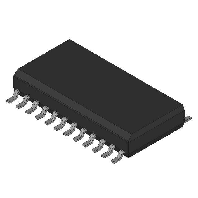
SO−24
DW SUFFIX
CASE 751E
24
1
MARKING DIAGRAMS
PDIP−24
These devices are available in Pb−free package(s). Specifications herein
apply to both standard and Pb−free devices. Please see our website at
www.onsemi.com for specific Pb−free orderable part numbers, or
contact your local ON Semiconductor sales office or representative.
REAL TIME TRANSFER
A-BUS TO B-BUS
REAL TIME TRANSFER
B-BUS TO A-BUS
A-BUS
A-BUS
REG
REG
REG
MC74ACT646N
AWLYYWW
SO−24
AC646
AWLYYWW
REG
B-BUS
B-BUS
Figure 1.
ACT646
AWLYYWW
Figure 2.
STORAGE
FROM BUS TO REGISTER
TRANSFER
FROM REGISTER TO BUS
A-BUS
A-BUS
REG
MC74AC646N
AWLYYWW
REG
REG
A
Location
L, WL
Y, YY
W, WW
Device
Figure 3.
B-BUS
Figure 4.
© Semiconductor Components Industries, LLC, 2006
March, 2006 − Rev. 6
= Wafer Lot
= Year
= Work Week
ORDERING INFORMATION
REG
B-BUS
= Assembly
1
Package
Shipping
MC74AC646N
PDIP−24
15 Units/Rail
MC74ACT646N
PDIP−24
15 Units/Rail
MC74AC646DW
SOIC−24
30 Units/Rail
MC74AC646DWR
2
MC74ACT646DW
SOIC−24 1000 Tape & Reel
SOIC−24
MC74ACT646DWR2
SOIC−24 1000 Tape & Reel
30 Units/Rail
Publication Order Number:
MC74AC646/D
�MC74AC646, MC74ACT646
VCC CBA SBA
24
1
23
2
22
3
CAB SAB DIR
G
B0
B1
B2
B3
B4
B5
B6
B7
21
20
19
18
17
16
15
14
13
4
5
6
7
8
9
10
11
12
A0
A1
A2
A3
A4
A5
A6
A7
GND
PIN ASSIGNMENT
PIN
FUNCTION
A0−A7
Data Register Inputs
Data Register A Outputs
B0−B7
Data Register B Inputs
Data Register B Outputs
CAB, CBA
Clock Pulse Inputs
SAB, SBA
Transmit/Receive Inputs
DIR, G
Output Enable Inputs
Figure 5. Pinout: 24−Lead Packages Conductors
(Top View)
CAB A0 A1 A2 A3 A4 A5 A6 A7
SAB
DIR
CBA
SBA
G
B0 B1 B2 B3 B4 B5 B6 B7
Figure 6. Logic Symbol
G
DIR
CBA
SBA
CAB
SAB
1 OF 8 CHANNELS
D0
C0
B0
A0
D0
C0
TO 7 OTHER CHANNELS
NOTE:
This diagram is provided only for the understanding of logic
operations and should not be used to estimate propagation delays.
Figure 7. Logic Diagram
http://onsemi.com
2
�MC74AC646, MC74ACT646
FUNCTION TABLE
Inputs
Data I/O*
Operation or Function
G
DIR
CAB
CBA
SAB
SBA
A0−A7
B0−B7
H
H
X
X
H or L
H or L
X
X
X
X
Input
Input
Isolation
Store A and B Data
L
L
L
L
X
X
X
X
X
X
L
H
Output
Input
Real Time B Data to A Bus
Stored B Data to A Bus
L
L
H
H
X
H or L
X
X
L
H
X
X
Input
Output
Real Time A Data to B Bus
Stored A Data to B Bus
*The data output functions may be enabled or disabled by various signals at the G and DIR inputs. Data input functions are always enabled;
i.e., data at the bus pins will be stored on every LOW−to−HIGH transition of the appropriate clock inputs.
NOTE: H = HIGH Voltage Level; L = LOW Voltage Level; X = Immaterial; = LOW−to−HIGH Transition
MAXIMUM RATINGS*
Symbol
Parameter
Value
Unit
−0.5 to +7.0
V
VCC
DC Supply Voltage (Referenced to GND)
Vin
DC Input Voltage (Referenced to GND)
−0.5 to VCC +0.5
V
Vout
DC Output Voltage (Referenced to GND)
−0.5 to VCC +0.5
V
Iin
DC Input Current, per Pin
±20
mA
Iout
DC Output Sink/Source Current, per Pin
±50
mA
ICC
DC VCC or GND Current per Output Pin
±50
mA
Tstg
Storage Temperature
−65 to +150
°C
*Maximum Ratings are those values beyond which damage to the device may occur. Functional operation should be restricted to the Recommended Operating Conditions.
RECOMMENDED OPERATING CONDITIONS
Symbol
Parameter
VCC
Supply Voltage
Vin, Vout
DC Input Voltage, Output Voltage (Ref. to GND)
tr, tf
Input Rise and Fall Time (Note 1)
′AC Devices except Schmitt Inputs
Min
Typ
Max
′AC
2.0
5.0
6.0
Unit
′ACT
4.5
5.0
5.5
0
−
VCC
VCC @ 3.0 V
−
150
−
VCC @ 4.5 V
−
40
−
VCC @ 5.5 V
−
25
−
VCC @ 4.5 V
−
10
−
VCC @ 5.5 V
−
8.0
−
−
−
140
°C
−40
25
85
°C
V
V
ns/V
tr, tf
Input Rise and Fall Time (Note 2)
′ACT Devices except Schmitt Inputs
TJ
Junction Temperature (PDIP)
TA
Operating Ambient Temperature Range
IOH
Output Current − High
−
−
−24
mA
IOL
Output Current − Low
−
−
24
mA
1. Vin from 30% to 70% VCC; see individual Data Sheets for devices that differ from the typical input rise and fall times.
2. Vin from 0.8 V to 2.0 V; see individual Data Sheets for devices that differ from the typical input rise and fall times.
http://onsemi.com
3
ns/V
�MC74AC646, MC74ACT646
DC CHARACTERISTICS
Symbol
Parameter
VCC
(V)
74AC
74AC
TA = +25°C
TA =
−40°C to
+85°C
Typ
Unit
Conditions
Guaranteed Limits
VIH
Minimum High Level
Input Voltage
3.0
4.5
5.5
1.5
2.25
2.75
2.1
3.15
3.85
2.1
3.15
3.85
V
VOUT = 0.1 V
or VCC − 0.1 V
VIL
Maximum Low Level
Input Voltage
3.0
4.5
5.5
1.5
2.25
2.75
0.9
1.35
1.65
0.9
1.35
1.65
V
VOUT = 0.1 V
or VCC − 0.1 V
VOH
Minimum High Level
Output Voltage
3.0
4.5
5.5
2.99
4.49
5.49
2.9
4.4
5.4
2.9
4.4
5.4
V
3.0
4.5
5.5
−
−
−
2.56
3.86
4.86
2.46
3.76
4.76
3.0
4.5
5.5
0.002
0.001
0.001
0.1
0.1
0.1
0.1
0.1
0.1
3.0
4.5
5.5
−
−
−
0.36
0.36
0.36
0.44
0.44
0.44
VOL
Maximum Low Level
Output Voltage
V
V
IOUT = −50 μA
*VIN = VIL or VIH
−12 mA
IOH
−24 mA
−24 mA
IOUT = 50 μA
V
*VIN = VIL or VIH
12 mA
IOL
24 mA
24 mA
IIN
Maximum Input
Leakage Current
5.5
−
±0.1
±1.0
μA
VI = VCC, GND
IOZT
Maximum
3-State
Current
5.5
−
±0.6
±6.0
μA
VI (OE) = VIL, VIH
VI = VCC, GND
VO = VCC, GND
5.5
−
−
75
mA
VOLD = 1.65 V Max
5.5
−
−
−75
mA
VOHD = 3.85 V Min
5.5
−
8.0
80
μA
VIN = VCC or GND
IOLD
IOHD
ICC
†Minimum Dynamic
Output Current
Maximum Quiescent
Supply Current
*All outputs loaded; thresholds on input associated with output under test.
†Maximum test duration 2.0 ms, one output loaded at a time.
NOTE: IIN and ICC @ 3.0 V are guaranteed to be less than or equal to the respective limit @ 5.5 V VCC.
http://onsemi.com
4
�MC74AC646, MC74ACT646
AC CHARACTERISTICS (For Figures and Waveforms − See Section 3 of the ON Semiconductor FACT Data Book, DL138/D)
Symbol
VCC*
(V)
Parameter
74AC
74AC
TA = +25°C
CL = 50 pF
TA = −40°C
to +85°C
CL = 50 pF
Min
Typ
Max
Min
Max
Unit
Fig.
No.
tPLH
Propagation Delay
Clock to Bus
3.3
5.0
4.0
2.5
10.5
7.5
16.5
12
3.0
2.0
18.5
13
ns
3−6
tPHL
Propagation Delay
Clock to Bus
3.3
5.0
3.0
2.0
9.5
6.5
14.5
10.5
2.5
1.5
16
11.5
ns
3−6
tPLH
Propagation Delay
Bus to Bus
3.3
5.0
2.5
1.5
7.5
5.0
12
8.0
2.0
1.0
13.5
9.0
ns
3−5
tPHL
Propagation Delay
Bus to Bus
3.3
5.0
1.5
1.5
7.5
5.0
12.5
9.0
1.5
1.0
13.5
9.5
ns
3−5
tPLH
Propagation Delay
SBA or SAB to An or Bn
(w/An or Bn HIGH or LOW)
3.3
5.0
2.0
1.5
8.5
6.0
13.5
10
1.5
1.5
15.5
11
ns
3−6
tPHL
Propagation Delay
SBA or SAB to An or Bn
(w/An or Bn HIGH or LOW)
3.3
5.0
1.5
1.5
8.5
6.0
13.5
10
1.5
1.5
15
11
ns
3−6
tPZH
Enable Time
G to An or Bn
3.3
5.0
2.5
1.5
7.0
5.0
11.5
8.5
2.0
1.5
12.5
9.0
ns
3−7
tPZL
Enable Time
G to An or Bn
3.3
5.0
2.5
1.5
7.5
5.5
12.5
9.0
2.0
1.5
14
10
ns
3−8
tPHZ
Disable Time
G to An or Bn
3.3
5.0
3.0
2.0
8.0
6.5
12.5
10
2.5
2.0
13.5
11
ns
3−7
tPLZ
Disable Time
G to An or Bn
3.3
5.0
2.0
1.5
7.5
6.0
12
9.5
2.0
1.5
13.5
10.5
ns
3−8
tPZH
Enable Time
DIR to An or Bn
3.3
5.0
2.0
1.5
6.5
5.0
11
7.5
1.5
1.0
12
8.5
ns
3−7
tPZL
Enable Time
DIR to An or Bn
3.3
5.0
2.5
1.5
7.0
5.0
11.5
8.0
2.0
1.0
13
9.0
ns
3−8
tPHZ
Disable Time
DIR to An or Bn
3.3
5.0
2.5
1.5
7.5
5.5
11.5
9.5
1.5
1.5
12.5
10
ns
3−7
tPLZ
Disable Time
DIR to An or Bn
3.3
5.0
1.5
1.5
7.5
5.5
12
9.5
1.5
1.5
13.5
10.5
ns
3−8
*Voltage Range 3.3 V is 3.3 V ±0.3 V.
Voltage Range 5.0 V is 5.0 V ±0.5 V.
http://onsemi.com
5
�MC74AC646, MC74ACT646
AC OPERATING REQUIREMENTS
Symbol
VCC*
(V)
Parameter
Typ
74AC
74AC
TA = +25°C
CL = 50 pF
TA = −40°C
to +85°C
CL = 50 pF
Unit
Fig.
No.
Guaranteed Minimum
ts
Setup Time, HIGH or LOW
Bus to Clock
3.3
5.0
2.0
1.5
5.0
4.0
5.5
4.5
ns
3−9
th
Hold Time, HIGH or LOW
Bus to Clock
3.3
5.0
−1.5
−0.5
0
0.5
0
1.0
ns
3−9
tw
Clock Pulse Width
HIGH or LOW
3.3
5.0
2.0
2.0
3.5
3.5
4.5
3.5
ns
3−6
*Voltage Range 3.3 V is 3.3 V ±0.3 V.
Voltage Range 5.0 V is 5.0 V ±0.5 V.
DC CHARACTERISTICS
Symbol
Parameter
VCC
(V)
74ACT
74ACT
TA = +25°C
TA =
−40°C to
+85°C
Typ
Guaranteed Limits
Unit
Conditions
VIH
Minimum High Level
Input Voltage
4.5
5.5
1.5
1.5
2.0
2.0
2.0
2.0
V
VOUT = 0.1 V
or VCC − 0.1 V
VIL
Maximum Low Level
Input Voltage
4.5
5.5
1.5
1.5
0.8
0.8
0.8
0.8
V
VOUT = 0.1 V
or VCC − 0.1 V
VOH
Minimum High Level
Output Voltage
4.5
5.5
4.49
5.49
4.4
5.4
4.4
5.4
V
4.5
5.5
−
−
3.86
4.86
3.76
4.76
4.5
5.5
0.001
0.001
0.1
0.1
0.1
0.1
4.5
5.5
−
−
0.36
0.36
0.44
0.44
V
*VIN = VIL or VIH
24 mA
IOL
24 mA
VOL
Maximum Low Level
Output Voltage
V
V
IOUT = −50 μA
*VIN = VIL or VIH
−24 mA
IOH
−24 mA
IOUT = 50 μA
IIN
Maximum Input
Leakage Current
5.5
−
±0.1
±1.0
μA
VI = VCC, GND
ΔICCT
Additional Max. ICC/Input
5.5
0.6
−
1.5
mA
VI = VCC − 2.1 V
IOZT
Maximum
3-State
Current
5.5
−
±0.6
±6.0
μA
VI (OE) = VIL, VIH
VI = VCC, GND
VO = VCC, GND
5.5
−
−
75
mA
VOLD = 1.65 V Max
5.5
−
−
−75
mA
VOHD = 3.85 V Min
5.5
−
8.0
80
μA
VIN = VCC or GND
IOLD
IOHD
ICC
†Minimum Dynamic
Output Current
Maximum Quiescent
Supply Current
*All outputs loaded; thresholds on input associated with output under test.
†Maximum test duration 2.0 ms, one output loaded at a time.
http://onsemi.com
6
�MC74AC646, MC74ACT646
AC CHARACTERISTICS (For Figures and Waveforms − See Section 3 of the ON Semiconductor FACT Data Book, DL138/D)
Symbol
VCC*
(V)
Parameter
74ACT
74ACT
TA = +25°C
CL = 50 pF
TA = −40°C
to +85°C
CL = 50 pF
Min
Typ
Max
Min
Max
Unit
Fig.
No.
tPLH
Propagation Delay
Clock to Bus
5.0
3.5
12.0
14.5
3.0
16.0
ns
3−6
tPHL
Propagation Delay
Clock to Bus
5.0
4.0
12.0
14.5
3.5
16.0
ns
3−6
tPLH
Propagation Delay
Bus to Bus
5.0
3.0
8.5
11.0
2.5
12.0
ns
3−5
tPHL
Propagation Delay
Bus to Bus
5.0
2.5
8.5
11.0
2.0
12.0
ns
3−5
tPLH
Propagation Delay
SBA or SAB to An or Bn
(w/An or Bn HIGH or LOW)
5.0
3.0
9.5
12.0
2.5
13.0
ns
3−6
tPHL
Propagation Delay
SBA or SAB to An or Bn
(w/An or Bn HIGH or LOW)
5.0
3.0
9.5
12.0
2.5
13.0
ns
3−6
tPZH
Enable Time
G to An or Bn
5.0
2.0
9.0
11.0
1.5
12.0
ns
3−7
tPZL
Enable Time
G to An or Bn
5.0
3.5
9.0
11.0
3.0
12.0
ns
3−8
tPHZ
Disable Time
G to An or Bn
5.0
5.0
10.5
13.0
4.5
14.5
ns
3−7
tPLZ
Disable Time
G to An or Bn
5.0
3.5
10.0
12.5
3.0
14.0
ns
3−8
tPZH
Enable Time
DIR to An or Bn
5.0
2.0
6.5
12.5
1.5
13.5
ns
3−7
tPZL
Enable Time
DIR to An or Bn
5.0
3.5
6.5
12.5
3.0
13.5
ns
3−8
tPHZ
Disable Time
DIR to An or Bn
5.0
5.0
8.5
12.5
4.5
13.5
ns
3−7
tPLZ
Disable Time
DIR to An or Bn
5.0
3.5
8.5
12.5
3.0
13.5
ns
3−8
*Voltage Range 5.0 V is 5.0 V ±0.5 V.
http://onsemi.com
7
�MC74AC646, MC74ACT646
AC OPERATING REQUIREMENTS
Symbol
VCC*
(V)
Parameter
74ACT
74ACT
TA = +25°C
CL = 50 pF
TA = −40°C
to +85°C
CL = 50 pF
Typ
Unit
Fig.
No.
Guaranteed Minimum
ts
Setup Time, HIGH or LOW
Bus to Clock
5.0
−
7.0
8.0
ns
3−9
th
Hold Time, HIGH or LOW
Bus to Clock
5.0
−
2.5
2.5
ns
3−9
tw
Clock Pulse Width
HIGH or LOW
5.0
−
7.0
8.0
ns
3−6
*Voltage Range 5.0 V is 5.0 V ±0.5 V.
CAPACITANCE
Symbol
Parameter
Value
Typ
Unit
Test Conditions
CIN
Input Capacitance
4.5
pF
VCC = 5.0 V
CI/O
Input/Output Capacitance
15
pF
VCC = 5.0 V
CPD
Power Dissipation Capacitance
60
pF
VCC = 5.0 V
http://onsemi.com
8
�MC74AC646, MC74ACT646
PACKAGE DIMENSIONS
PDIP−24
N SUFFIX
24 PIN PLASTIC DIP PACKAGE
CASE 724−03
ISSUE D
−A−
24
13
1
12
NOTES:
1. CHAMFERED CONTOUR OPTIONAL.
2. DIMENSION L TO CENTER OF LEADS WHEN
FORMED PARALLEL.
3. DIMENSIONING AND TOLERANCING PER ANSI
Y14.5M, 1982.
4. CONTROLLING DIMENSION: INCH.
−B−
L
C
−T−
NOTE 1
K
SEATING
PLANE
N
E
G
M
J
F
D
24 PL
0.25 (0.010)
24 PL
0.25 (0.010)
M
T A
M
T B
M
M
DIM
A
B
C
D
E
F
G
J
K
L
M
N
INCHES
MIN
MAX
1.230
1.265
0.250
0.270
0.145
0.175
0.015
0.020
0.050 BSC
0.040
0.060
0.100 BSC
0.007
0.012
0.110
0.140
0.300 BSC
0_
15_
0.020
0.040
MILLIMETERS
MIN
MAX
31.25
32.13
6.35
6.85
3.69
4.44
0.38
0.51
1.27 BSC
1.02
1.52
2.54 BSC
0.18
0.30
2.80
3.55
7.62 BSC
0_
15_
0.51
1.01
SO−24
DW SUFFIX
24 PIN PLASTIC SOIC PACKAGE
CASE 751E−04
ISSUE E
−A−
24
NOTES:
1. DIMENSIONING AND TOLERANCING PER ANSI
Y14.5M, 1982.
2. CONTROLLING DIMENSION: MILLIMETER.
3. DIMENSIONS A AND B DO NOT INCLUDE
MOLD PROTRUSION.
4. MAXIMUM MOLD PROTRUSION 0.15 (0.006)
PER SIDE.
5. DIMENSION D DOES NOT INCLUDE DAMBAR
PROTRUSION. ALLOWABLE DAMBAR
PROTRUSION SHALL BE 0.13 (0.005) TOTAL IN
EXCESS OF D DIMENSION AT MAXIMUM
MATERIAL CONDITION.
13
−B−
12X
P
0.010 (0.25)
1
M
B
M
12
24X
D
J
0.010 (0.25)
M
T A
S
B
S
F
R
C
−T−
SEATING
PLANE
22X
G
K
M
http://onsemi.com
9
X 45 _
DIM
A
B
C
D
F
G
J
K
M
P
R
MILLIMETERS
MIN
MAX
15.25
15.54
7.40
7.60
2.35
2.65
0.35
0.49
0.41
0.90
1.27 BSC
0.23
0.32
0.13
0.29
0_
8_
10.05
10.55
0.25
0.75
INCHES
MIN
MAX
0.601
0.612
0.292
0.299
0.093
0.104
0.014
0.019
0.016
0.035
0.050 BSC
0.009
0.013
0.005
0.011
0_
8_
0.395
0.415
0.010
0.029
�MC74AC646, MC74ACT646
Notes
http://onsemi.com
10
�MC74AC646, MC74ACT646
Notes
ON Semiconductor and
are registered trademarks of Semiconductor Components Industries, LLC (SCILLC). SCILLC reserves the right to make changes without further notice
to any products herein. SCILLC makes no warranty, representation or guarantee regarding the suitability of its products for any particular purpose, nor does SCILLC assume any liability
arising out of the application or use of any product or circuit, and specifically disclaims any and all liability, including without limitation special, consequential or incidental damages.
“Typical” parameters which may be provided in SCILLC data sheets and/or specifications can and do vary in different applications and actual performance may vary over time. All
operating parameters, including “Typicals” must be validated for each customer application by customer’s technical experts. SCILLC does not convey any license under its patent rights
nor the rights of others. SCILLC products are not designed, intended, or authorized for use as components in systems intended for surgical implant into the body, or other applications
intended to support or sustain life, or for any other application in which the failure of the SCILLC product could create a situation where personal injury or death may occur. Should
Buyer purchase or use SCILLC products for any such unintended or unauthorized application, Buyer shall indemnify and hold SCILLC and its officers, employees, subsidiaries, affiliates,
and distributors harmless against all claims, costs, damages, and expenses, and reasonable attorney fees arising out of, directly or indirectly, any claim of personal injury or death
associated with such unintended or unauthorized use, even if such claim alleges that SCILLC was negligent regarding the design or manufacture of the part. SCILLC is an Equal
Opportunity/Affirmative Action Employer. This literature is subject to all applicable copyright laws and is not for resale in any manner.
PUBLICATION ORDERING INFORMATION
LITERATURE FULFILLMENT:
Literature Distribution Center for ON Semiconductor
P.O. Box 61312, Phoenix, Arizona 85082−1312 USA
Phone: 480−829−7710 or 800−344−3860 Toll Free USA/Canada
Fax: 480−829−7709 or 800−344−3867 Toll Free USA/Canada
Email: orderlit@onsemi.com
N. American Technical Support: 800−282−9855 Toll Free
USA/Canada
Japan: ON Semiconductor, Japan Customer Focus Center
2−9−1 Kamimeguro, Meguro−ku, Tokyo, Japan 153−0051
Phone: 81−3−5773−3850
http://onsemi.com
11
ON Semiconductor Website: http://onsemi.com
Order Literature: http://www.onsemi.com/litorder
For additional information, please contact your
local Sales Representative.
MC74AC646/D
�


 工商网监
湘ICP备2023018690号
工商网监
湘ICP备2023018690号
