ON Semiconductor
Is Now
To learn more about onsemi™, please visit our website at
www.onsemi.com
onsemi and and other names, marks, and brands are registered and/or common law trademarks of Semiconductor Components Industries, LLC dba “onsemi” or its affiliates and/or
subsidiaries in the United States and/or other countries. onsemi owns the rights to a number of patents, trademarks, copyrights, trade secrets, and other intellectual property. A listing of onsemi
product/patent coverage may be accessed at www.onsemi.com/site/pdf/Patent-Marking.pdf. onsemi reserves the right to make changes at any time to any products or information herein, without
notice. The information herein is provided “as-is” and onsemi makes no warranty, representation or guarantee regarding the accuracy of the information, product features, availability, functionality,
or suitability of its products for any particular purpose, nor does onsemi assume any liability arising out of the application or use of any product or circuit, and specifically disclaims any and all
liability, including without limitation special, consequential or incidental damages. Buyer is responsible for its products and applications using onsemi products, including compliance with all laws,
regulations and safety requirements or standards, regardless of any support or applications information provided by onsemi. “Typical” parameters which may be provided in onsemi data sheets and/
or specifications can and do vary in different applications and actual performance may vary over time. All operating parameters, including “Typicals” must be validated for each customer application
by customer’s technical experts. onsemi does not convey any license under any of its intellectual property rights nor the rights of others. onsemi products are not designed, intended, or authorized
for use as a critical component in life support systems or any FDA Class 3 medical devices or medical devices with a same or similar classification in a foreign jurisdiction or any devices intended for
implantation in the human body. Should Buyer purchase or use onsemi products for any such unintended or unauthorized application, Buyer shall indemnify and hold onsemi and its officers, employees,
subsidiaries, affiliates, and distributors harmless against all claims, costs, damages, and expenses, and reasonable attorney fees arising out of, directly or indirectly, any claim of personal injury or death
associated with such unintended or unauthorized use, even if such claim alleges that onsemi was negligent regarding the design or manufacture of the part. onsemi is an Equal Opportunity/Affirmative
Action Employer. This literature is subject to all applicable copyright laws and is not for resale in any manner. Other names and brands may be claimed as the property of others.
�MC74AC652, MC74ACT652
Octal Transceiver/Register
with 3-State Outputs
(Non-Inverting)
The MC74AC/ACT652 consists of registered bus transceiver
circuits, with outputs, D−type flip−flops and control circuitry
providing multiplexed transmission of data directly from the input bus
or from the internal storage registers. Data on the A or B bus will be
loaded into the respective registers on the LOW−to−HIGH transition
of the appropriate clock pin (CAB or CBA). The four fundamental
data handling functions available are illustrated in Figures 1 to 4.
Features
•
•
•
•
•
•
•
•
www.onsemi.com
MARKING DIAGRAMS
AC652
AWLYYWWG
24
1
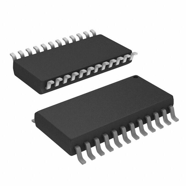
SO−24
DW SUFFIX
CASE 751E
Independent Registers for A and B Buses
Multiplexed Real−Time and Stored Data Transfers
Choice of True and Inverting Data Paths
3−State Outputs
300 mil Slim Dual−in−Line Package
Outputs Source/Sink 24 mA
′ACT652 Has TTL Compatible Inputs
These are Pb−Free Devices
A
WL
YY
WW
G
ACT652
AWLYYWWG
= Assembly Location
= Wafer Lot
= Year
= Work Week
= Pb−Free Package
ORDERING INFORMATION
REAL TIME TRANSFER
A‐BUS TO B‐BUS
REAL TIME TRANSFER
B‐BUS TO A‐BUS
A‐BUS
REG
A‐BUS
REG
REG
REG
B‐BUS
B‐BUS
Figure 1.
Figure 2.
STORAGE
FROM BUS TO REGISTER
TRANSFER
FROM REGISTER TO BUS
A‐BUS
A‐BUS
REG
REG
REG
REG
B‐BUS
B‐BUS
Figure 3.
Figure 4.
© Semiconductor Components Industries, LLC, 2015
March, 2015 − Rev. 7
See detailed ordering and shipping information in the package
dimensions section on page 9 of this data sheet.
1
Publication Order Number:
MC74AC652/D
�MC74AC652, MC74ACT652
VCC
CBA
SBA
GBA
B0
B1
B2
B3
B4
B5
B6
B7
24
23
22
21
20
19
18
17
16
15
14
13
PIN ASSIGNMENT
1
2
3
4
5
6
7
8
9
10
11
12
CAB
SAB
GAB
A0
A1
A2
A3
A4
A5
A6
A7
GND
PIN
FUNCTION
A0−A7
Data Register A Inputs
Data Register A Outputs
B0−B7
Data Register B Inputs
Data Register B Outputs
CAB, CBA
Clock Pulse Inputs
SAB, SBA
Transmit/Receive Inputs
GAB, GBA
Output Enable Inputs
Figure 5. Pinout: 24−Lead Plastic Package
(Top View)
CAB
SAB
GAB
CBA
SBA
GBA
B0
B1
B2
B3
B4
B5
B6
B7
A0
A1
A2
A3
A4
A5
A6
A7
Figure 6. Logic Symbol
GBA
GAB
CBA
SBA
CAB
SAB
1 OF 8 CHANNELS
D0
C0
B0
A0
D0
C0
TO 7 OTHER CHANNELS
NOTE:
This diagram is provided only for the understanding of
logic operations and should not be used to estimate
propagation delays.
Figure 7. Logic Diagram
www.onsemi.com
2
�MC74AC652, MC74ACT652
FUNCTION TABLE
Inputs
Data I/O*
Operation or Function
GAB
GBA
CAB
CBA
SAB
SBA
A0 − A7
B0 − B7
L
L
H
H
H or L
⇑
H or L
⇑
X
X
X
X
Input
Input
X
H
H
H
⇑
⇑
H or L
⇑
X
X**
X
X
Input
Input
L
L
X
L
H or L
⇑
⇑
⇑
X
X
X
X**
Unspecified*
Output
Input
Input
Hold A, Store B
Store B in Both Registers
L
L
L
L
X
X
X
H or L
X
X
L
H
Output
Input
Real-Time B Data to A Bus
Stored B Data to A Bus
H
H
H
H
X
H or L
X
X
L
H
X
X
Input
Output
Real-Time A Data to B Bus
Stored A Data to B Bus
H
L
H or L
H or L
H
H
Output
Output
Stored A Data to B Bus and
Stored B Data to A Bus
Isolation
Store A and B Data
Unspecified* Store A, Hold B
Output
Store A in Both Registers
*The data output functions may be enabled or disabled by various signals at the GBA and GAB inputs. Data input functions are always enabled;
i.e., data at the bus pins will be stored on every LOW-to-HIGH transition of the appropriate clock inputs.
**Select control = L: clocks can occur simultaneously.
H = HIGH Voltage Level; L = LOW Voltage Level; X = Immaterial; ⇑ = LOW-to-HIGH Transition
www.onsemi.com
3
�MC74AC652, MC74ACT652
MAXIMUM RATINGS
Symbol
Parameter
Value
Unit
−0.5 to +7.0
V
VCC
DC Supply Voltage (Referenced to GND)
VIN
DC Input Voltage (Referenced to GND)
−0.5 to VCC +0.5
V
DC Output Voltage (Referenced to GND) (Note 1)
−0.5 to VCC +0.5
V
VOUT
IIK
DC Input Diode Current
±20
mA
IOK
DC Output Diode Current
±50
mA
IOUT
DC Output Sink/Source Current
±50
mA
ICC
DC Supply Current, per Output Pin
±50
mA
IGND
DC Ground Current, per Output Pin
±100
mA
TSTG
Storage Temperature Range
*65 to )150
_C
TL
Lead temperature, 1 mm from Case for 10 Seconds
260
_C
TJ
Junction Temperature Under Bias
140
_C
qJA
Thermal Resistance (Note 2)
59.8
_C/W
MSL
Moisture Sensitivity
FR
Flammability Rating
VESD
ILatchup
Level 1
Oxygen Index: 30% − 35%
ESD Withstand Voltage
UL 94 V−0 @ 0.125 in
Human Body Model (Note 3)
Machine Model (Note 4)
Charged Device Model (Note 5)
Latchup Performance
Above VCC and Below GND at 85_C (Note 6)
> 2000
> 200
> 1000
V
±100
mA
Stresses exceeding those listed in the Maximum Ratings table may damage the device. If any of these limits are exceeded, device functionality
should not be assumed, damage may occur and reliability may be affected.
1. IOUT absolute maximum rating must be observed.
2. The package thermal impedance is calculated in accordance with JESD 51−7.
3. Tested to EIA/JESD22−A114−A.
4. Tested to EIA/JESD22−A115−A.
5. Tested to JESD22−C101−A.
6. Tested to EIA/JESD78.
RECOMMENDED OPERATING CONDITIONS
Symbol
Parameter
VCC
Supply Voltage
Vin, Vout
DC Input Voltage, Output Voltage (Ref. to GND)
tr, tf
Input Rise and Fall Time (Note 1)
′AC Devices except Schmitt Inputs
Min
Typ
Min
Unit
′AC
2.0
5.0
6.0
′ACT
4.5
5.0
5.5
0
−
VCC
VCC @ 3.0 V
−
150
−
VCC @ 4.5 V
−
40
−
VCC @ 5.5 V
−
25
−
VCC @ 4.5 V
−
10
−
VCC @ 5.5 V
−
8.0
−
−40
25
85
°C
V
V
ns/V
tr, tf
Input Rise and Fall Time (Note 2)
′ACT Devices except Schmitt Inputs
TA
Operating Ambient Temperature Range
IOH
Output Current — HIGH
−
−
−24
mA
IOL
Output Current — LOW
−
−
24
mA
ns/V
Functional operation above the stresses listed in the Recommended Operating Ranges is not implied. Extended exposure to stresses beyond
the Recommended Operating Ranges limits may affect device reliability.
1. Vin from 30% to 70% VCC; see individual Data Sheets for devices that differ from the typical input rise and fall times.
2. Vin from 0.8 V to 2.0 V; see individual Data Sheets for devices that differ from the typical input rise and fall times.
www.onsemi.com
4
�MC74AC652, MC74ACT652
DC CHARACTERISTICS
Symbol
Parameter
VCC
(V)
74AC
74AC
TA = +25°C
TA =
−40°C to
+85°C
Typ
VIH
VIL
VOH
VOL
Unit
Conditions
Guaranteed Limits
Minimum High Level
Input Voltage
3.0
4.5
5.5
1.5
2.25
2.75
2.1
3.15
3.85
2.1
3.15
3.85
V
VOUT = 0.1 V
or VCC − 0.1 V
Maximum Low Level
Input Voltage
3.0
4.5
5.5
1.5
2.25
2.75
0.9
1.35
1.65
0.9
1.35
1.65
V
VOUT = 0.1 V
or VCC − 0.1 V
Minimum High Level
Output Voltage
3.0
4.5
5.5
2.99
4.49
5.49
2.9
4.4
5.4
2.9
4.4
5.4
V
3.0
4.5
5.5
−
−
−
2.56
3.86
4.86
2.46
3.76
4.76
3.0
4.5
5.5
0.002
0.001
0.001
0.1
0.1
0.1
0.1
0.1
0.1
3.0
4.5
5.5
−
−
−
0.36
0.36
0.36
0.44
0.44
0.44
Minimum Low Level
Output Voltage
IOUT = − 50 μA
V
*VIN = VIL or VIH
− 12 mA
IOH
− 24 mA
− 24 mA
IOUT = 50 μA
V
V
*VIN = VIL or VIH
12 mA
IOL
24 mA
24 mA
IIN
Maximum Input
Leakage Current
5.5
−
±0.1
±1.0
μA
IOZT
Maximum
3-State
Current
5.5
−
±0.6
±6.0
μA
VI (OE) = VIL, VIH
VI = VCC, GND
VO= VCC, GND
5.5
−
−
75
mA
VOLD = 1.65 V Max
5.5
−
−
−75
mA
VOHD = 3.85 V Min
5.5
−
8.0
80
μA
VIN = VCC or GND
IOLD
IOHD
ICC
†Minimum Dynamic
Output Current
Maximum Quiescent
Supply Current
*All outputs loaded; thresholds on input associated with output under test.
†Maximum test duration 2.0 ms, one input loaded at a time.
NOTE: IIN and ICC @ 3.0 V are guaranteed to be less than or equal to the respective limit @ 5.5 V.
www.onsemi.com
5
VI = VCC, GND
�MC74AC652, MC74ACT652
AC CHARACTERISTICS
Symbol
VCC*
(V)
Parameter
74AC
74AC
TA = +25°C
CL = 50 pF
TA = −40°C
to +85°C
CL = 50 pF
Min
Max
Min
Max
Unit
tPLH
Propagation Delay
CPBA or CPAB to An or Bn
3.0
5.0
4.0
2.5
17.0
12.0
3.0
2.0
19.0
14.0
ns
tPHL
Propagation Delay
CPBA or CPAB to An or Bn
3.0
5.0
3.0
2.0
14.5
10.5
2.5
1.5
16.5
12.0
ns
tPLH
Propagation Delay
A or B to Bn or An
3.0
5.0
3.0
2.0
14.0
9.5
2.5
1.5
16.0
11.0
ns
tPHL
Propagation Delay
A or B to Bn or An
3.0
5.0
2.5
1.5
13.0
9.0
2.0
1.0
15.0
10.5
ns
tPLH
Propagation Delay
SBA or SAB to An or Bn
3.0
5.0
3.0
2.5
14.0
10.0
2.5
2.0
16.0
11.5
ns
tPHL
Propagation Delay
SBA or SAB to An or Bn
3.0
5.0
2.5
2.0
13.5
10.0
2.0
1.5
15.5
11.5
ns
tPZH
Output Enable Time
OEBA to An
3.0
5.0
2.5
1.5
12.0
9.0
2.0
1.0
13.5
10.0
ns
tPZL
Output Enable Time
OEBA to An
3.0
5.0
2.5
1.5
12.0
9.0
2.0
1.0
14.0
10.5
ns
tPHZ
Output Disable Time
OEBA to An
3.0
5.0
3.0
2.0
13.0
11.0
2.5
1.5
14.0
12.0
ns
tPLZ
Output Disable Time
OEBA to An
3.0
5.0
2.5
2.0
12.5
10.5
2.0
1.5
14.0
12.0
ns
*Voltage Range 3.3 V is 3.3 V ±0.3 V.
Voltage Range 5.0 V is 5.0 V ±0.5 V.
www.onsemi.com
6
�MC74AC652, MC74ACT652
DC CHARACTERISTICS
Symbol
Parameter
VCC
(V)
74ACT
74ACT
TA = +25°C
TA =
−40°C to
+85°C
Typ
Guaranteed Limits
Unit
Conditions
VIH
Minimum High Level
Input Voltage
4.5
5.5
1.5
1.5
2.0
2.0
2.0
2.0
V
VOUT = 0.1 V
or VCC − 0.1 V
VIL
Maximum Low Level
Input Voltage
4.5
5.5
1.5
1.5
0.8
0.8
0.8
0.8
V
VOUT = 0.1 V
or VCC − 0.1 V
VOH
Minimum High Level
Output Voltage
4.5
5.5
4.49
5.49
4.4
5.4
4.4
5.4
V
4.5
5.5
−
−
3.86
4.86
3.76
4.76
4.5
5.5
0.001
0.001
0.1
0.1
0.1
0.1
4.5
5.5
−
−
0.36
0.36
0.44
0.44
V
VOL
Minimum Low Level
Output Voltage
V
V
IOUT = − 50 μA
*VIN = VIL or VIH
− 24 mA
IOH
− 24 mA
IOUT = − 50 μA
*VIN = VIL or VIH
− 24 mA
IOH
− 24 mA
IIN
Maximum Input
Leakage Current
5.5
−
±0.1
±1.0
μA
VI = VCC, GND
ΔICCT
Additional Max. ICC/Input
5.5
0.6
−
1.5
mA
VI = VCC − 2.1 V
IOZT
Maximum
3-State
Current
5.5
−
±0.6
±6.0
μA
VI (OE) = VIL, VIH
VI = VCC, GND
VO = VCC, GND
5.5
−
−
75
mA
VOLD = 1.65 V Max
5.5
−
−
−75
mA
VOHD = 3.85 V Min
5.5
−
8.0
80
μA
VIN = VCC or GND
IOLD
IOHD
ICC
†Minimum Dynamic
Output Current
Maximum Quiescent
Supply Current
*All outputs loaded; thresholds on input associated with output under test.
†Maximum test duration 2.0 ms, one input loaded at a time.
www.onsemi.com
7
�MC74AC652, MC74ACT652
AC CHARACTERISTICS
Symbol
VCC*
(V)
Parameter
74ACT
74ACT
TA = +25°C
CL = 50 pF
TA = −40°C
to +85°C
CL = 50 pF
Min
Max
Min
Max
Unit
tPLH
Propagation Delay
CPBA or CPAB to An or Bn
5.0
4.0
14.5
3.5
16.5
ns
tPHL
Propagation Delay
CPBA or CPAB to An or Bn
5.0
3.5
14.5
3.0
16.5
ns
tPLH
Propagation Delay
A or B to Bn or An
5.0
2.5
11.5
2.0
13.0
ns
tPHL
Propagation Delay
A or B to Bn or An
5.0
2.5
11.5
2.0
13.0
ns
tPLH
Propagation Delay
SBA or SAB to An or Bn
5.0
2.5
12.0
2.0
13.5
ns
tPHL
Propagation Delay
SBA or SAB to An or Bn
5.0
3.0
12.0
2.5
13.5
ns
tPZH
Output Enable Time
OEBA to An
5.0
2.0
11.5
1.5
13.0
ns
tPZL
Output Enable Time
OEBA to An
5.0
2.5
11.5
2.0
13.0
ns
tPHZ
Output Disable Time
OEBA to An
5.0
3.0
13.0
2.5
14.0
ns
tPLZ
Output Disable Time
OEBA to An
5.0
2.5
12.5
2.0
14.0
ns
tPZH
Output Enable time
OEAB to Bn
5.0
2.5
12.0
2.0
13.5
ns
tPZL
Output Enable Time
OEAB to Bn
5.0
2.5
12.0
2.0
13.5
ns
tPHZ
Output Enable Time
OEAB to Bn
5.0
3.5
13.5
3.0
14.5
ns
tPLZ
Output Enable Time
OEAB to Bn
5.0
3.0
13.5
2.5
15.0
ns
ts
Setup Time, HIGH or LOW
An or Bn to CPBA or CPAB
5.0
7.0
−
8.0
−
ns
th
Hold Time, HIGH or LOW
An or Bn to CPBA or CPAB
5.0
2.5
−
2.5
−
ns
tw
CPAB, CPBA Pulse Width
HIGH or LOW
5.0
6.0
−
7.0
−
ns
*Voltage Range 3.3 V is 3.3 V ±0.3 V.
Voltage Range 5.0 V is 5.0 V ±0.5 V.
CAPACITANCE
Symbol
Parameter
74ACT
Typ
Unit
Test Conditions
CIN
Input Capacitance
4.5
pF
VCC = 5.0 V
CI/O
Input/Output Capacitance
15
pF
VCC = 5.0 V
CPD
Power Dissipation Capacitance
60.0
pF
VCC = 5.0 V
www.onsemi.com
8
�MC74AC652, MC74ACT652
ORDERING INFORMATION
Device
Package
Shipping†
SOIC−24
(Pb−Free)
1000 / Tape & Reel
MC74AC652DWG
MC74AC652DWR2G
MC74ACT652DWG
30 Units / Rail
30 Units / Rail
1000 / Tape & Reel
MC74ACT652DWR2G
†For information on tape and reel specifications, including part orientation and tape sizes, please refer to our Tape and Reel Packaging
Specifications Brochure, BRD8011/D.
www.onsemi.com
9
�MC74AC652, MC74ACT652
PACKAGE DIMENSIONS
SOIC−24 WB
DW SUFFIX
CASE 751E−04
ISSUE F
D
A
B
0.25 C
24
E
NOTES:
1. DIMENSIONING AND TOLERANCING PER ASME
Y14.5M, 1994.
2. CONTROLLING DIMENSION: MILLIMETERS.
3. DIMENSIONS b AND c APPLY TO THE FLAT SECTION OF THE LEAD AND ARE MEASURED BETWEEN 0.10 AND 0.25 FROM THE LEAD TIP.
4. DIMENSIONS D AND E1 DO NOT INCLUDE MOLD
FLASH, PROTRUSIONS OR GATE BURRS. MOLD
FLASH, PROTRUSIONS OR GATE BURRS SHALL
NOT EXCEED 0.15 mm PER SIDE. INTERLEAD
FLASH OR PROTRUSION SHALL NOT EXCEED
0.25 PER SIDE. DIMENSIONS D AND E1 ARE
DETERMINED AT DATUM H.
5. A1 IS DEFINED AS THE VERTICAL DISTANCE
FROM THE SEATING PLANE TO THE LOWEST
POINT ON THE PACKAGE BODY.
H
13
E1
1
L
12
C
DETAIL A
24X b
PIN 1
INDICATOR
0.25
TOP VIEW
M
C A
S
B
S
h
x 45 _
A
A1
DIM
A
A1
b
c
D
E
E1
e
h
L
M
NOTE 3
e
C
NOTE 5
M
c
SEATING
PLANE
NOTE 3
DETAIL A
END VIEW
SIDE VIEW
MILLIMETERS
MIN
MAX
2.35
2.65
0.13
0.29
0.35
0.49
0.23
0.32
15.25
15.54
10.30 BSC
7.40
7.60
1.27 BSC
0.25
0.75
0.41
0.90
0_
8_
RECOMMENDED
SOLDERING FOOTPRINT*
24X
24X
1.62
0.52
11.00
1
1.27
PITCH
DIMENSIONS: MILLIMETERS
*For additional information on our Pb−Free strategy and soldering
details, please download the ON Semiconductor Soldering and
Mounting Techniques Reference Manual, SOLDERRM/D.
ON Semiconductor and the
are registered trademarks of Semiconductor Components Industries, LLC (SCILLC) or its subsidiaries in the United States and/or other countries.
SCILLC owns the rights to a number of patents, trademarks, copyrights, trade secrets, and other intellectual property. A listing of SCILLC’s product/patent coverage may be accessed
at www.onsemi.com/site/pdf/Patent−Marking.pdf. SCILLC reserves the right to make changes without further notice to any products herein. SCILLC makes no warranty, representation
or guarantee regarding the suitability of its products for any particular purpose, nor does SCILLC assume any liability arising out of the application or use of any product or circuit, and
specifically disclaims any and all liability, including without limitation special, consequential or incidental damages. “Typical” parameters which may be provided in SCILLC data sheets
and/or specifications can and do vary in different applications and actual performance may vary over time. All operating parameters, including “Typicals” must be validated for each
customer application by customer’s technical experts. SCILLC does not convey any license under its patent rights nor the rights of others. SCILLC products are not designed, intended,
or authorized for use as components in systems intended for surgical implant into the body, or other applications intended to support or sustain life, or for any other application in which
the failure of the SCILLC product could create a situation where personal injury or death may occur. Should Buyer purchase or use SCILLC products for any such unintended or
unauthorized application, Buyer shall indemnify and hold SCILLC and its officers, employees, subsidiaries, affiliates, and distributors harmless against all claims, costs, damages, and
expenses, and reasonable attorney fees arising out of, directly or indirectly, any claim of personal injury or death associated with such unintended or unauthorized use, even if such claim
alleges that SCILLC was negligent regarding the design or manufacture of the part. SCILLC is an Equal Opportunity/Affirmative Action Employer. This literature is subject to all applicable
copyright laws and is not for resale in any manner.
PUBLICATION ORDERING INFORMATION
LITERATURE FULFILLMENT:
Literature Distribution Center for ON Semiconductor
P.O. Box 5163, Denver, Colorado 80217 USA
Phone: 303−675−2175 or 800−344−3860 Toll Free USA/Canada
Fax: 303−675−2176 or 800−344−3867 Toll Free USA/Canada
Email: orderlit@onsemi.com
N. American Technical Support: 800−282−9855 Toll Free
USA/Canada
Europe, Middle East and Africa Technical Support:
Phone: 421 33 790 2910
Japan Customer Focus Center
Phone: 81−3−5817−1050
www.onsemi.com
10
ON Semiconductor Website: www.onsemi.com
Order Literature: http://www.onsemi.com/orderlit
For additional information, please contact your local
Sales Representative
MC74AC652/D
�


 工商网监
湘ICP备2023018690号
工商网监
湘ICP备2023018690号
