MC74HC125A,
MC74HC126A
Quad 3−State Noninverting
Buffers
High−Performance Silicon−Gate CMOS
http://onsemi.com
The MC74HC125A and MC74HC126A are identical in pinout to
the LS125 and LS126. The device inputs are compatible with standard
CMOS outputs; with pullup resistors, they are compatible with
LSTTL outputs.
The HC125A and HC126A noninverting buffers are designed to be
used with 3−state memory address drivers, clock drivers, and other
bus−oriented systems. The devices have four separate output enables
that are active−low (HC125A) or active−high (HC126A).
•
•
•
•
•
•
•
MARKING
DIAGRAMS
14
PDIP−14
N SUFFIX
CASE 646
1
14
Output Drive Capability: 15 LSTTL Loads
Outputs Directly Interface to CMOS, NMOS, and TTL
Operating Voltage Range: 2.0 to 6.0 V
Low Input Current: 1.0 µA
High Noise Immunity Characteristic of CMOS Devices
In Compliance with the Requirements Defined by JEDEC Standard
No. 7A
Chip Complexity: 72 FETs or 18 Equivalent Gates
LOGIC DIAGRAM
HC125A
HC126A
Active−Low Output Enables
Active−High Output Enables
A1
OE1
A2
OE2
A3
OE3
A4
OE4
2
3
1
2
A1
Y1
6
4
9
8
Y3
10
9
A3
11
13
8
11
12
A4
Y4
PIN 14 = VCC
PIN 7 = GND
Output
Inputs
Output
OE
Y
A
OE
Y
H
L
X
L
L
H
H
L
Z
H
L
X
H
H
L
H
L
Z
March, 2000 − Rev. 9
HC
12xA
ALYW
TSSOP−14
DT SUFFIX
CASE 948G
1
A
= Assembly Location
WL or L = Wafer Lot
YY or Y = Year
WW or W = Work Week
Y3
OE1
1
14
VCC
A1
2
13
OE4
Y1
3
12
A4
OE2
4
11
Y4
A2
5
10
OE3
Y2
6
9
A3
GND
7
8
Y3
Y4
Device
HC126A
A
Semiconductor Components Industries, LLC, 2000
14
ORDERING INFORMATION
FUNCTION TABLE
Inputs
1
13
OE4
HC125A
Y2
10
OE3
12
6
4
OE2
HC12xA
AWLYWW
PIN ASSIGNMENT
5
A2
Y2
Y1
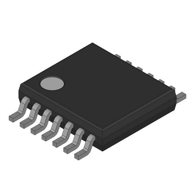
SOIC−14
D SUFFIX
CASE 751A
1
OE1
5
3
MC74HC12xAN
AWLYYWW
Package
Shipping
MC74HC12xAN
PDIP−14
2000 / Box
MC74HC12xAD
SOIC−14
55 / Rail
MC74HC12xADR2
47
SOIC−14
2500 / Reel
MC74HC12xADT
TSSOP−14
96 / Rail
MC74HC12xADTR2
TSSOP−14
2500 / Reel
Publication Order Number:
MC74HC125A/D
�MC74HC125A, MC74HC126A
ÎÎÎÎÎÎÎÎÎÎÎÎÎÎÎÎÎÎÎÎÎÎÎ
ÎÎÎÎ
ÎÎÎÎÎÎÎÎÎÎÎÎÎÎ
ÎÎÎÎÎ
ÎÎÎ
ÎÎÎÎÎÎÎÎÎÎÎÎÎÎÎÎÎÎÎÎÎÎÎ
ÎÎÎÎ
ÎÎÎÎÎÎÎÎÎÎÎÎÎÎ
ÎÎÎÎÎ
ÎÎÎ
ÎÎÎÎ
ÎÎÎÎÎÎÎÎÎÎÎÎÎÎ
ÎÎÎÎÎ
ÎÎÎ
ÎÎÎÎ
ÎÎÎÎÎÎÎÎÎÎÎÎÎÎ
ÎÎÎÎÎ
ÎÎÎ
ÎÎÎÎ
ÎÎÎÎÎÎÎÎÎÎÎÎÎÎ
ÎÎÎÎÎ
ÎÎÎ
ÎÎÎÎ
ÎÎÎÎÎÎÎÎÎÎÎÎÎÎ
ÎÎÎÎÎ
ÎÎÎ
ÎÎÎÎ
ÎÎÎÎÎÎÎÎÎÎÎÎÎÎ
ÎÎÎÎÎ
ÎÎÎ
ÎÎÎÎ
ÎÎÎÎÎÎÎÎÎÎÎÎÎÎ
ÎÎÎÎÎ
ÎÎÎ
ÎÎÎÎ
ÎÎÎÎÎÎÎÎÎÎÎÎÎÎ
ÎÎÎÎÎ
ÎÎÎ
ÎÎÎÎ
ÎÎÎÎÎÎÎÎÎÎÎÎÎÎ
ÎÎÎÎÎ
ÎÎÎ
ÎÎÎÎ
ÎÎÎÎÎÎÎÎÎÎÎÎÎÎ
ÎÎÎÎÎ
ÎÎÎ
ÎÎÎÎ
ÎÎÎÎÎÎÎÎÎÎÎÎÎÎ
ÎÎÎÎÎ
ÎÎÎ
MAXIMUM RATINGS*
Symbol
VCC
Parameter
DC Supply Voltage (Referenced to GND)
Value
Unit
– 0.5 to + 7.0
V
V
Vin
DC Input Voltage (Referenced to GND)
– 0.5 to VCC + 0.5
Vout
DC Output Voltage (Referenced to GND)
Iin
– 0.5 to VCC + 0.5
V
DC Input Current, per Pin
± 20
mA
Iout
DC Output Current, per Pin
± 35
mA
ICC
DC Supply Current, VCC and GND Pins
± 75
mA
PD
Power Dissipation in Still Air
750
500
450
mW
Tstg
Storage Temperature
– 65 to + 150
�C
Plastic DIP†
SOIC Package†
TSSOP Package†
This device contains protection
circuitry to guard against damage
due to high static voltages or electric
fields. However, precautions must
be taken to avoid applications of any
voltage higher than maximum rated
voltages to this high−impedance circuit. For proper operation, Vin and
Vout should be constrained to the
range GND � (Vin or Vout) � VCC.
Unused inputs must always be
tied to an appropriate logic voltage
level (e.g., either GND or VCC).
Unused outputs must be left open.
Lead Temperature, 1 mm from Case for 10 Seconds
�C
(Plastic DIP, SOIC or TSSOP Package)
260
*Maximum Ratings are those values beyond which damage to the device may occur.
Functional operation should be restricted to the Recommended Operating Conditions.
†Derating — Plastic DIP: – 10 mW/�C from 65� to 125�C
SOIC Package: – 7 mW/�C from 65� to 125�C
TSSOP Package: – 6.1 mW/�C from 65� to 125�C
For high frequency or heavy load considerations, see Chapter 2 of the ON Semiconductor High−Speed CMOS Data Book (DL129/D).
TL
ÎÎÎÎ
ÎÎÎÎÎÎÎÎÎÎÎÎÎÎÎ
ÎÎÎ
ÎÎ
ÎÎÎ
ÎÎÎÎ
ÎÎÎÎÎÎÎÎÎÎÎÎÎÎÎ
ÎÎÎ
ÎÎ
ÎÎÎ
ÎÎÎÎ
ÎÎÎÎÎÎÎÎÎÎÎÎÎÎÎ
ÎÎÎ
ÎÎ
ÎÎÎ
ÎÎÎÎ
ÎÎÎÎÎÎÎÎÎÎÎÎÎÎÎ
ÎÎÎ
ÎÎ
ÎÎÎ
ÎÎÎÎ
ÎÎÎÎÎÎÎÎÎÎÎÎÎÎÎ
ÎÎÎ
ÎÎ
ÎÎÎ
ÎÎÎÎ
ÎÎÎÎÎÎÎÎÎÎÎÎÎÎÎ
ÎÎÎ
ÎÎ
ÎÎÎ
ÎÎÎÎ
ÎÎÎÎÎÎÎÎÎÎÎÎÎÎÎ
ÎÎÎÎÎ
ÎÎÎ
ÎÎÎÎ
ÎÎÎÎÎÎÎÎÎ
ÎÎÎÎÎÎÎÎÎ
ÎÎÎÎ
ÎÎÎÎÎÎÎÎÎ
ÎÎÎ
ÎÎÎÎ
ÎÎÎÎÎÎÎÎÎ
ÎÎÎÎÎÎÎÎÎ
ÎÎÎÎ
ÎÎÎÎ
ÎÎÎ
ÎÎÎÎ
ÎÎÎ
ÎÎÎÎÎÎÎÎÎ
ÎÎÎÎ
ÎÎÎÎÎÎÎÎÎ
ÎÎÎÎÎÎÎÎÎ
ÎÎÎÎ
ÎÎÎÎ
ÎÎÎ
ÎÎÎÎ
ÎÎÎ
ÎÎÎÎ
ÎÎÎÎÎÎÎÎÎ
ÎÎÎÎÎÎÎÎÎ
ÎÎÎÎ
ÎÎÎÎ
ÎÎÎ
ÎÎÎÎ
ÎÎÎ
ÎÎÎÎ
ÎÎÎÎÎÎÎÎÎ
ÎÎÎÎÎÎÎÎÎ
ÎÎÎÎ
ÎÎÎÎ
ÎÎÎ
ÎÎÎÎ
ÎÎÎ
ÎÎÎÎ
ÎÎÎÎÎÎÎÎÎ
ÎÎÎÎÎÎÎÎÎ
ÎÎÎÎ
ÎÎÎÎ
ÎÎÎ
ÎÎÎÎ
ÎÎÎ
ÎÎÎÎ
ÎÎÎÎÎÎÎÎÎ
ÎÎÎÎÎÎÎÎÎ
ÎÎÎÎ
ÎÎÎÎ
ÎÎÎ
ÎÎÎÎ
ÎÎÎ
ÎÎÎÎ
ÎÎÎÎÎÎÎÎÎ
ÎÎÎÎÎÎÎÎÎ
ÎÎÎÎ
ÎÎÎÎ
ÎÎÎ
ÎÎÎÎ
ÎÎÎ
ÎÎÎÎ
ÎÎÎÎÎÎÎÎÎ
ÎÎÎÎÎÎÎÎÎ
ÎÎÎÎ
ÎÎÎÎ
ÎÎÎ
ÎÎÎÎ
ÎÎÎ
ÎÎÎÎ
ÎÎÎÎÎÎÎÎÎ
ÎÎÎÎÎÎÎÎÎ
ÎÎÎÎ
ÎÎÎÎ
ÎÎÎ
ÎÎÎÎ
ÎÎÎ
ÎÎÎÎ
ÎÎÎÎÎÎÎÎÎ
ÎÎÎÎÎÎÎÎÎ
ÎÎÎÎ
ÎÎÎÎ
ÎÎÎ
ÎÎÎÎ
ÎÎÎ
ÎÎÎÎ
ÎÎÎÎÎÎÎÎÎ
ÎÎÎÎÎÎÎÎÎ
ÎÎÎÎ
ÎÎÎÎ
ÎÎÎ
ÎÎÎÎ
ÎÎÎ
ÎÎÎÎ
ÎÎÎÎÎÎÎÎÎ
ÎÎÎÎÎÎÎÎÎ
ÎÎÎÎ
ÎÎÎÎ
ÎÎÎ
ÎÎÎÎ
ÎÎÎ
ÎÎÎÎ
ÎÎÎÎÎÎÎÎÎ
ÎÎÎÎÎÎÎÎÎ
ÎÎÎÎ
ÎÎÎÎ
ÎÎÎ
ÎÎÎÎ
ÎÎÎ
ÎÎÎÎ
ÎÎÎÎÎÎÎÎÎ
ÎÎÎÎÎÎÎÎÎ
ÎÎÎÎ
ÎÎÎÎ
ÎÎÎ
ÎÎÎÎ
ÎÎÎ
ÎÎÎÎ
ÎÎÎÎÎÎÎÎÎ
ÎÎÎÎÎÎÎÎÎ
ÎÎÎÎ
ÎÎÎÎ
ÎÎÎ
ÎÎÎÎ
ÎÎÎ
ÎÎÎÎ
ÎÎÎÎÎÎÎÎÎ
ÎÎÎÎÎÎÎÎÎ
ÎÎÎÎ
ÎÎÎÎ
ÎÎÎ
ÎÎÎÎ
ÎÎÎ
ÎÎÎÎ
ÎÎÎÎÎÎÎÎÎ
ÎÎÎÎÎÎÎÎÎ
ÎÎÎÎ
ÎÎÎÎ
ÎÎÎ
ÎÎÎÎ
ÎÎÎ
RECOMMENDED OPERATING CONDITIONS
Symbol
VCC
Vin, Vout
TA
tr, tf
Parameter
Min
Max
Unit
2.0
6.0
V
0
VCC
V
– 55
+ 125
�C
0
0
0
1000
500
400
ns
DC Supply Voltage (Referenced to GND)
DC Input Voltage, Output Voltage
(Referenced to GND)
Operating Temperature, All Package Types
Input Rise and Fall Time
(Figure 1)
VCC = 2.0 V
VCC = 4.5 V
VCC = 6.0 V
DC ELECTRICAL CHARACTERISTICS (Voltages Referenced to GND)
Guaranteed Limit
VCC
V
– 55 to
25�C
� 85�C
� 125�C
Unit
VIH
Minimum High−Level Input
Voltage
Vout = VCC – 0.1 V
|Iout| � 20 µA
2.0
3.0
4.5
6.0
1.5
2.1
3.15
4.2
1.5
2.1
3.15
4.2
1.5
2.1
3.15
4.2
V
VIL
Maximum Low−Level Input
Voltage
Vout = 0.1 V
|Iout| � 20 µA
2.0
3.0
4.5
6.0
0.5
0.9
1.35
1.8
0.5
0.9
1.35
1.8
0.5
0.9
1.35
1.8
V
Minimum High−Level Output
Voltage
Vin = VIH
|Iout| � 20 µA
2.0
4.5
6.0
1.9
4.4
5.9
1.9
4.4
5.9
1.9
4.4
5.9
V
3.0
4.5
6.0
2.48
3.98
5.48
2.34
3.84
5.34
2.2
3.7
5.2
2.0
4.5
6.0
0.1
0.1
0.1
0.1
0.1
0.1
0.1
0.1
0.1
3.0
4.5
6.0
0.26
0.26
0.26
0.33
0.33
0.33
0.4
0.4
0.4
Symbol
VOH
Parameter
Test Conditions
|Iout| � 3.6 mA
|Iout| � 6.0 mA
|Iout| � 7.8 mA
Vin = VIH
VOL
Maximum Low−Level Output
Voltage
Vin = VIL
|Iout| � 20 µA
Vin = VIL
|Iout| � 3.6 mA
|Iout| � 6.0 mA
|Iout| � 7.8 mA
http://onsemi.com
48
V
�MC74HC125A, MC74HC126A
ÎÎÎÎ
ÎÎÎÎÎÎÎÎÎ
ÎÎÎÎÎÎÎÎÎ
ÎÎÎÎ
ÎÎÎÎÎÎÎÎÎ
ÎÎÎ
ÎÎÎÎ
ÎÎÎÎÎÎÎÎÎ
ÎÎÎÎÎÎÎÎÎ
ÎÎÎÎ
ÎÎÎÎ
ÎÎÎ
ÎÎÎÎ
ÎÎÎ
ÎÎÎÎÎÎÎÎÎ
ÎÎÎÎ
ÎÎÎÎÎÎÎÎÎ
ÎÎÎÎÎÎÎÎÎ
ÎÎÎÎ
ÎÎÎÎ
ÎÎÎ
ÎÎÎÎ
ÎÎÎ
ÎÎÎÎ
ÎÎÎÎÎÎÎÎÎ
ÎÎÎÎÎÎÎÎÎ
ÎÎÎÎ
ÎÎÎÎ
ÎÎÎ
ÎÎÎÎ
ÎÎÎ
ÎÎÎÎ
ÎÎÎÎÎÎÎÎÎ
ÎÎÎÎÎÎÎÎÎ
ÎÎÎÎ
ÎÎÎÎ
ÎÎÎ
ÎÎÎÎ
ÎÎÎ
ÎÎÎÎ
ÎÎÎÎÎÎÎÎÎ
ÎÎÎÎÎÎÎÎÎ
ÎÎÎÎ
ÎÎÎÎ
ÎÎÎ
ÎÎÎÎ
ÎÎÎ
ÎÎÎÎ
ÎÎÎÎÎÎÎÎÎ
ÎÎÎÎÎÎÎÎÎ
ÎÎÎÎ
ÎÎÎÎ
ÎÎÎ
ÎÎÎÎ
ÎÎÎ
ÎÎÎÎ
ÎÎÎÎÎÎÎÎÎ
ÎÎÎÎÎÎÎÎÎ
ÎÎÎÎ
ÎÎÎÎ
ÎÎÎ
ÎÎÎÎ
ÎÎÎ
ÎÎÎÎ
ÎÎÎÎÎÎÎÎÎ
ÎÎÎÎÎÎÎÎÎ
ÎÎÎÎ
ÎÎÎÎ
ÎÎÎ
ÎÎÎÎ
ÎÎÎ
ÎÎÎÎÎ
ÎÎÎÎÎÎÎÎÎÎÎÎÎÎÎÎ
ÎÎÎÎ
ÎÎÎÎÎÎÎÎÎ
ÎÎÎ
ÎÎÎÎÎ
ÎÎÎÎÎÎÎÎÎÎÎÎÎÎÎÎ
ÎÎÎÎ
ÎÎÎÎ
ÎÎÎ
ÎÎÎÎ
ÎÎÎ
ÎÎÎÎÎÎÎÎÎ
ÎÎÎÎÎ
ÎÎÎÎÎÎÎÎÎÎÎÎÎÎÎÎ
ÎÎÎÎ
ÎÎÎÎ
ÎÎÎ
ÎÎÎÎ
ÎÎÎ
ÎÎÎÎÎ
ÎÎÎÎÎÎÎÎÎÎÎÎÎÎÎÎ
ÎÎÎÎ
ÎÎÎÎ
ÎÎÎ
ÎÎÎÎ
ÎÎÎ
ÎÎÎÎÎ
ÎÎÎÎÎÎÎÎÎÎÎÎÎÎÎÎ
ÎÎÎÎ
ÎÎÎÎ
ÎÎÎ
ÎÎÎÎ
ÎÎÎ
ÎÎÎÎÎ
ÎÎÎÎÎÎÎÎÎÎÎÎÎÎÎÎ
ÎÎÎÎ
ÎÎÎÎ
ÎÎÎ
ÎÎÎÎ
ÎÎÎ
ÎÎÎÎÎ
ÎÎÎÎÎÎÎÎÎÎÎÎÎÎÎÎ
ÎÎÎÎ
ÎÎÎÎ
ÎÎÎ
ÎÎÎÎ
ÎÎÎ
ÎÎÎÎÎ
ÎÎÎÎÎÎÎÎÎÎÎÎÎÎÎÎ
ÎÎÎÎ
ÎÎÎÎ
ÎÎÎ
ÎÎÎÎ
ÎÎÎ
ÎÎÎÎÎ
ÎÎÎÎÎÎÎÎÎÎÎÎÎÎÎÎ
ÎÎÎÎ
ÎÎÎÎ
ÎÎÎ
ÎÎÎÎ
ÎÎÎ
ÎÎÎÎÎ
ÎÎÎÎÎÎÎÎÎÎÎÎÎÎÎÎ
ÎÎÎÎ
ÎÎÎÎ
ÎÎÎ
ÎÎÎÎ
ÎÎÎ
ÎÎÎÎÎ
ÎÎÎÎÎÎÎÎÎÎÎÎÎÎÎÎ
ÎÎÎÎ
ÎÎÎÎ
ÎÎÎ
ÎÎÎÎ
ÎÎÎ
ÎÎÎÎÎ
ÎÎÎÎÎÎÎÎÎÎÎÎÎÎÎÎ
ÎÎÎÎ
ÎÎÎÎ
ÎÎÎ
ÎÎÎÎ
ÎÎÎ
ÎÎÎÎÎ
ÎÎÎÎÎÎÎÎÎÎÎÎÎÎÎÎ
ÎÎÎÎ
ÎÎÎÎ
ÎÎÎ
ÎÎÎÎ
ÎÎÎ
ÎÎÎÎÎ
ÎÎÎÎÎÎÎÎÎÎÎÎÎÎÎÎ
ÎÎÎÎ
ÎÎÎÎ
ÎÎÎ
ÎÎÎÎ
ÎÎÎ
ÎÎÎÎÎ
ÎÎÎÎÎÎÎÎÎÎÎÎÎÎÎÎ
ÎÎÎÎ
ÎÎÎÎ
ÎÎÎ
ÎÎÎÎ
ÎÎÎ
ÎÎÎÎÎ
ÎÎÎÎÎÎÎÎÎÎÎÎÎÎÎÎ
ÎÎÎÎ
ÎÎÎÎ
ÎÎÎ
ÎÎÎÎ
ÎÎÎ
ÎÎÎÎÎ
ÎÎÎÎÎÎÎÎÎÎÎÎÎÎÎÎ
ÎÎÎÎ
ÎÎÎÎ
ÎÎÎ
ÎÎÎÎ
ÎÎÎ
ÎÎÎÎÎ
ÎÎÎÎÎÎÎÎÎÎÎÎÎÎÎÎ
ÎÎÎÎ
ÎÎÎÎ
ÎÎÎ
ÎÎÎÎ
ÎÎÎ
DC ELECTRICAL CHARACTERISTICS (Voltages Referenced to GND)
Guaranteed Limit
Symbol
Parameter
Test Conditions
VCC
V
– 55 to
25�C
� 85�C
� 125�C
Unit
Maximum Input Leakage
Current
Vin = VCC or GND
6.0
± 0.1
± 1.0
± 1.0
µA
IOZ
Maximum Three−State
Leakage Current
Output in High−Impedance State
Vin = VIL or VIH
Vout = VCC or GND
6.0
± 0.5
± 5.0
± 10
µA
ICC
Maximum Quiescent Supply
Current (per Package)
Vin = VCC or GND
Iout = 0 µA
6.0
4.0
40
160
µA
Iin
NOTE: Information on typical parametric values can be found in Chapter 2 of the ON Semiconductor High−Speed CMOS Data Book
(DL129/D).
AC ELECTRICAL CHARACTERISTICS (CL = 50 pF, Input tr = tf = 6.0 ns)
Guaranteed Limit
Symbol
Parameter
VCC
V
– 55 to
25�C
� 85�C
� 125�C
Unit
tPLH,
tPHL
Maximum Propagation Delay, Input A to Output Y
(Figures 1 and 3)
2.0
3.0
4.5
6.0
90
36
18
15
115
45
23
20
135
60
27
23
ns
tPLZ,
tPHZ
Maximum Propagation Delay, Output Enable to Y
(Figures 2 and 4)
2.0
3.0
4.5
6.0
120
45
24
20
150
60
30
26
180
80
36
31
ns
tPZL,
tPZH
Maximum Propagation Delay, Output Enable to Y
(Figures 2 and 4)
2.0
3.0
4.5
6.0
90
36
18
15
115
45
23
20
135
60
27
23
ns
tTLH,
tTHL
Maximum Output Transition Time, Any Output
(Figures 1 and 3)
2.0
3.0
4.5
6.0
60
22
12
10
75
28
15
13
90
34
18
15
ns
Maximum Input Capacitance
—
10
10
10
pF
Maximum Three−State Output Capacitance
(Output in High−Impedance State)
—
15
15
15
pF
Cin
Cout
NOTE: For propagation delays with loads other than 50 pF, and information on typical parametric values, see Chapter 2 of the ON
Semiconductor High−Speed CMOS Data Book (DL129/D).
Typical @ 25°C, VCC = 5.0 V
30
pF
2
* Used to determine the no−load dynamic power consumption: PD = CPD VCC f + ICC VCC . For load considerations, see Chapter 2 of the
ON Semiconductor High−Speed CMOS Data Book (DL129/D).
CPD
Power Dissipation Capacitance (Per Buffer)*
http://onsemi.com
49
�MC74HC125A, MC74HC126A
SWITCHING WAVEFORMS
OE (HC125A)
tr
tf
OUTPUT Y
GND
VCC
90%
50%
10%
INPUT A
VCC
OE (HC126A)
GND
50%
GND
tPHL
tPLH
VCC
50%
tPZL tPLZ
90%
50%
10%
OUTPUT Y
tTHL
tTLH
HIGH
IMPEDANCE
50%
10%
VOL
90%
VOH
HIGH
IMPEDANCE
tPZH tPHZ
50%
OUTPUT Y
Figure 1.
Figure 2.
TEST POINT
TEST POINT
OUTPUT
DEVICE
UNDER
TEST
DEVICE
UNDER
TEST
CL*
*Includes all probe and jig capacitance
OUTPUT
1 kΩ
CL *
CONNECT TO VCC WHEN
TESTING tPLZ AND tPZL.
CONNECT TO GND WHEN
TESTING tPHZ and tPZH.
*Includes all probe and jig capacitance
Figure 3. Test Circuit
Figure 4. Test Circuit
VCC
OE
A
Y
HC125A
(1/4 OF THE DEVICE)
VCC
OE
A
Y
HC126A
(1/4 OF THE DEVICE)
http://onsemi.com
50
�
很抱歉,暂时无法提供与“MC74HC126ADT”相匹配的价格&库存,您可以联系我们找货
免费人工找货