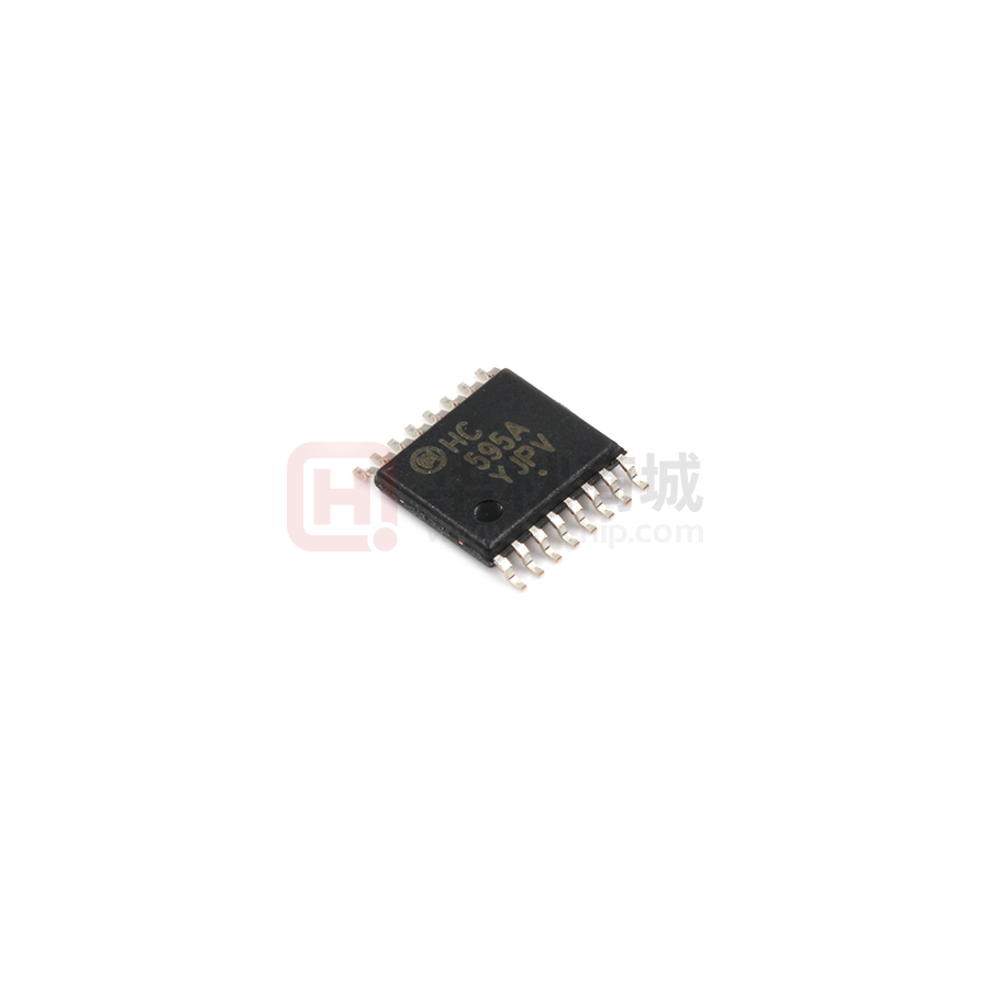
MC74HC595A
8-Bit Serial-Input/Serial or
Parallel-Output Shift
Register with Latched
3-State Outputs
www.onsemi.com
High−Performance Silicon−Gate CMOS
The MC74HC595A consists of an 8−bit shift register and an 8−bit
D−type latch with three−state parallel outputs. The shift register
accepts serial data and provides a serial output. The shift register also
provides parallel data to the 8−bit latch. The shift register and latch
have independent clock inputs. This device also has an asynchronous
reset for the shift register.
The HC595A directly interfaces with the SPI serial data port on
CMOS MPUs and MCUs.
SOIC−16
D SUFFIX
CASE 751B
1
QFN16
MN SUFFIX
CASE 485AW
Features
•
•
•
•
•
•
•
•
•
•
Output Drive Capability: 15 LSTTL Loads
Outputs Directly Interface to CMOS, NMOS, and TTL
Operating Voltage Range: 2.0 to 6.0 V
Low Input Current: 1.0 mA
High Noise Immunity Characteristic of CMOS Devices
In Compliance with the Requirements Defined by JEDEC
Standard No. 7 A
Chip Complexity: 328 FETs or 82 Equivalent Gates
Improvements over HC595
♦ Improved Propagation Delays
♦ 50% Lower Quiescent Power
♦ Improved Input Noise and Latchup Immunity
NLV Prefix for Automotive and Other Applications Requiring
Unique Site and Control Change Requirements; AEC−Q100
Qualified and PPAP Capable
These Devices are Pb−Free, Halogen Free and are RoHS Compliant
TSSOP−16
DT SUFFIX
CASE 948F
MARKING DIAGRAMS
16
16
HC
595A
ALYWG
G
HC595AG
AWLYWW
1
1
SOIC−16
TSSOP−16
595A
ALYWG
G
QFN16*
*V595A marking used for
NLV74HC595AMN1TWG
A
WL, L
YY, Y
WW, W
G, G
= Assembly Location
= Wafer Lot
= Year
= Work Week
= Pb−Free Package
(Note: Microdot may be in either location)
ORDERING INFORMATION
See detailed ordering and shipping information in the package
dimensions section on page 10 of this data sheet.
© Semiconductor Components Industries, LLC, 2016
December, 2016 − Rev. 23
1
Publication Order Number:
MC74HC595A/D
�MC74HC595A
QB VCC
1 16
QB
1
16
VCC
QC
2
15
QA
QC
2
15 QA
QD
3
14
A
QD
3
14 A
QE
4
13
OUTPUT ENABLE
QE
4
QF
5
QG
QH
GND
13 OUTPUT ENABLE
GND
12
LATCH CLOCK
QF
5
12 LATCH CLOCK
6
11
SHIFT CLOCK
QG
6
11 SHIFT CLOCK
7
10
RESET
QH
7
8
9
10 RESET
8
9
GND SQH
SQH
SOIC, TSSOP
QFN
Figure 1. Pin Assignments
LOGIC DIAGRAM
SERIAL
DATA
INPUT
A
14
15
1
2
3
4
SHIFT
REGISTER
LATCH
5
6
7
SHIFT 11
CLOCK
10
RESET
9
LATCH 12
CLOCK
OUTPUT 13
ENABLE
QA
QB
QC
QD
QE
QF
QG
QH
SQH
VCC = PIN 16
GND = PIN 8
www.onsemi.com
2
PARALLEL
DATA
OUTPUTS
SERIAL
DATA
OUTPUT
�MC74HC595A
MAXIMUM RATINGS
Symbol
Parameter
Value
Unit
–0.5 to +7.0
V
VCC
DC Supply Voltage (Referenced to GND)
Vin
DC Input Voltage (Referenced to GND)
–0.5 to VCC+0.5
V
Vout
DC Output Voltage (Referenced to GND)
–0.5 to VCC+0.5
V
Iin
DC Input Current, per Pin
±20
mA
Iout
DC Output Current, per Pin
±35
mA
ICC
DC Supply Current, VCC and GND Pins
±75
mA
PD
Power Dissipation in Still Air,
500
450
mW
Tstg
Storage Temperature
–65 to +150
_C
TL
Lead Temperature, 1 mm from Case for 10 Seconds
(Plastic DIP, SOIC or TSSOP Package)
260
ESD Withstand Voltage Human Body Model (Note 1)
Machine Model (Note 2)
Charged Device Model (Note 3)
> 3000
> 400
N/A
VESD
SOIC Package†
TSSOP Package†
This device contains protection
circuitry to guard against damage
due to high static voltages or electric
fields. However, precautions must
be taken to avoid applications of any
voltage higher than maximum rated
voltages to this high−impedance circuit. For proper operation, Vin and
Vout should be constrained to the
range GND v (Vin or Vout) v VCC.
Unused inputs must always be
tied to an appropriate logic voltage
level (e.g., either GND or VCC).
Unused outputs must be left open.
_C
V
Stresses exceeding those listed in the Maximum Ratings table may damage the device. If any
of these limits are exceeded, device functionality should not be assumed, damage may occur
and reliability may be affected.
†Derating: SOIC Package: –7 mW/_C from 65_ to 125_C
TSSOP Package: −6.1 mW/_C from 65_ to 125_C
1. Tested to EIA/JESD22−A114−A.
2. Tested to EIA/JESD22−A115−A.
3. Tested to JESD22−C101−A.
RECOMMENDED OPERATING CONDITIONS
Symbol
VCC
Vin, Vout
Parameter
DC Supply Voltage (Referenced to GND)
DC Input Voltage, Output Voltage
(Referenced to GND)
TA
Operating Temperature, All Package Types
tr, tf
Input Rise and Fall Time
(Figure 1)
VCC = 2.0 V
VCC = 4.5 V
VCC = 6.0 V
Min
Max
Unit
2.0
6.0
V
0
VCC
V
–55
+125
_C
0
0
0
1000
500
400
ns
Functional operation above the stresses listed in the Recommended Operating Ranges is not implied. Extended exposure to stresses beyond
the Recommended Operating Ranges limits may affect device reliability.
www.onsemi.com
3
�MC74HC595A
DC ELECTRICAL CHARACTERISTICS (Voltages Referenced to GND)
VCC
V
Guaranteed Limit
–55 to 25_C
≤ 85_C
≤ 125_C
Unit
VIH
Minimum High−Level Input
Voltage
Vout = 0.1 V or VCC – 0.1 V
|Iout| ≤ 20 mA
2.0
3.0
4.5
6.0
1.5
2.1
3.15
4.2
1.5
2.1
3.15
4.2
1.5
2.1
3.15
4.2
V
VIL
Maximum Low−Level Input
Voltage
Vout = 0.1 V or VCC – 0.1 V
|Iout| ≤ 20 mA
2.0
3.0
4.5
6.0
0.5
0.9
1.35
1.8
0.5
0.9
1.35
1.8
0.5
0.9
1.35
1.8
V
VOH
Minimum High−Level Output
Voltage, QA − QH
Vin = VIH or VIL
|Iout| ≤ 20 mA
2.0
4.5
6.0
1.9
4.4
5.9
1.9
4.4
5.9
1.9
4.4
5.9
V
3.0
4.5
6.0
2.48
3.98
5.48
2.34
3.84
5.34
2.2
3.7
5.2
2.0
4.5
6.0
0.1
0.1
0.1
0.1
0.1
0.1
0.1
0.1
0.1
3.0
4.5
6.0
0.26
0.26
0.26
0.33
0.33
0.33
0.4
0.4
0.4
2.0
4.5
6.0
1.9
4.4
5.9
1.9
4.4
5.9
1.9
4.4
5.9
3.0
4.5
6.0
2.48
3.98
5.48
2.34
3.84
5.34
2.2
3.7
5.2
2.0
4.5
6.0
0.1
0.1
0.1
0.1
0.1
0.1
0.1
0.1
0.1
3.0
4.5
6.0
0.26
0.26
0.26
0.33
0.33
0.33
0.4
0.4
0.4
Symbol
Parameter
Test Conditions
Vin = VIH or VIL
VOL
Maximum Low−Level Output
Voltage, QA − QH
Vin = VIH or VIL
|Iout| ≤ 20 mA
Vin = VIH or VIL
VOH
Minimum High−Level Output
Voltage, SQH
Maximum Low−Level Output
Voltage, SQH
|Iout| ≤ 2.4 mA
|Iout| ≤ 6.0 mA
|Iout| ≤ 7.8 mA
Vin = VIH or VIL
IIoutI ≤ 20 mA
Vin = VIH or VIL
VOL
|Iout| ≤ 2.4 mA
|Iout| ≤ 6.0 mA
|Iout| ≤ 7.8 mA
|Iout| ≤ 2.4 mA
IIoutI ≤ 4.0 mA
IioutI ≤ 5.2 mA
Vin = VIH or VIL
IIoutI ≤ 20 mA
Vin = VIH or VIL
|Iout| ≤ 2.4 mA
IIoutI ≤ 4.0 mA
IioutI ≤ 5.2 mA
V
V
V
Iin
Maximum Input Leakage
Current
Vin = VCC or GND
6.0
±0.1
±1.0
±1.0
mA
IOZ
Maximum Three−State
Leakage
Current, QA − QH
Output in High−Impedance State
Vin = VIL or VIH
Vout = VCC or GND
6.0
±0.5
±5.0
±10
mA
ICC
Maximum Quiescent Supply
Current (per Package)
Vin = VCC or GND
lout = 0 mA
6.0
4.0
40
160
mA
www.onsemi.com
4
�MC74HC595A
AC ELECTRICAL CHARACTERISTICS (CL = 50 pF, Input tr = tf = 6.0 ns)
VCC
V
Guaranteed Limit
–55 to 25_C
≤ 85_C
≤ 125_C
Unit
fmax
Maximum Clock Frequency (50% Duty Cycle)
(Figures 1 and 7)
2.0
3.0
4.5
6.0
6.0
15
30
35
4.8
10
24
28
4.0
8.0
20
24
MHz
tPLH,
tPHL
Maximum Propagation Delay, Shift Clock to SQH
(Figures 1 and 7)
2.0
3.0
4.5
6.0
140
100
28
24
175
125
35
30
210
150
42
36
ns
tPHL
Maximum Propagation Delay, Reset to SQH
(Figures 2 and 7)
2.0
3.0
4.5
6.0
145
100
29
25
180
125
36
31
220
150
44
38
ns
tPLH,
tPHL
Maximum Propagation Delay, Latch Clock to QA − QH
(Figures 3 and 7)
2.0
3.0
4.5
6.0
140
100
28
24
175
125
35
30
210
150
42
36
ns
tPLZ,
tPHZ
Maximum Propagation Delay, Output Enable to QA − QH
(Figures 4 and 8)
2.0
3.0
4.5
6.0
150
100
30
26
190
125
38
33
225
150
45
38
ns
tPZL,
tPZH
Maximum Propagation Delay, Output Enable to QA − QH
(Figures 4 and 8)
2.0
3.0
4.5
6.0
135
90
27
23
170
110
34
29
205
130
41
35
ns
tTLH,
tTHL
Maximum Output Transition Time, QA − QH
(Figures 3 and 7)
2.0
3.0
4.5
6.0
60
23
12
10
75
27
15
13
90
31
18
15
ns
tTLH,
tTHL
Maximum Output Transition Time, SQH
(Figures 1 and 7)
2.0
3.0
4.5
6.0
75
27
15
13
95
32
19
16
110
36
22
19
ns
Symbol
Parameter
Cin
Maximum Input Capacitance
−
10
10
10
pF
Cout
Maximum Three−State Output Capacitance (Output in
High−Impedance State), QA − QH
−
15
15
15
pF
Typical @ 25°C, VCC = 5.0 V
CPD
300
Power Dissipation Capacitance (Per Package)*
www.onsemi.com
5
pF
�MC74HC595A
TIMING REQUIREMENTS (Input tr = tf = 6.0 ns)
VCC
V
Guaranteed Limit
25_C to –55_C
≤ 85_C
≤ 125_C
Unit
tsu
Minimum Setup Time, Serial Data Input A to Shift Clock
(Figure 5)
2.0
3.0
4.5
6.0
50
40
10
9.0
65
50
13
11
75
60
15
13
ns
tsu
Minimum Setup Time, Shift Clock to Latch Clock
(Figure 6)
2.0
3.0
4.5
6.0
75
60
15
13
95
70
19
16
110
80
22
19
ns
th
Minimum Hold Time, Shift Clock to Serial Data Input A
(Figure 5)
2.0
3.0
4.5
6.0
5.0
5.0
5.0
5.0
5.0
5.0
5.0
5.0
5.0
5.0
5.0
5.0
ns
trec
Minimum Recovery Time, Reset Inactive to Shift Clock
(Figure 2)
2.0
3.0
4.5
6.0
50
40
10
9.0
65
50
13
11
75
60
15
13
ns
tw
Minimum Pulse Width, Reset
(Figure 2)
2.0
3.0
4.5
6.0
60
45
12
10
75
60
15
13
90
70
18
15
ns
tw
Minimum Pulse Width, Shift Clock
(Figure 1)
2.0
3.0
4.5
6.0
50
40
10
9.0
65
50
13
11
75
60
15
13
ns
tw
Minimum Pulse Width, Latch Clock
(Figure 6)
2.0
3.0
4.5
6.0
50
40
10
9.0
65
50
13
11
75
60
15
13
ns
tr, tf
Maximum Input Rise and Fall Times
(Figure 1)
2.0
3.0
4.5
6.0
1000
800
500
400
1000
800
500
400
1000
800
500
400
ns
Symbol
Parameter
www.onsemi.com
6
�MC74HC595A
FUNCTION TABLE
Inputs
Operation
Reset
Resulting Function
Serial
Input
A
Shift
Clock
Latch
Clock
Output
Enable
Shift
Register
Contents
Latch
Register
Contents
Serial
Output
SQH
Parallel
Outputs
QA − QH
Reset shift register
L
X
X
L, H, ↓
L
L
U
L
U
Shift data into shift
register
H
D
↑
L, H, ↓
L
D → SRA;
SRN → SRN+1
U
SRG → SRH
U
Shift register remains
unchanged
H
X
L, H, ↓
L, H, ↓
L
U
U
U
U
Transfer shift register
contents to latch
register
H
X
L, H, ↓
↑
L
U
SRN → LRN
U
SRN
Latch register remains
unchanged
X
X
X
L, H, ↓
L
*
U
*
U
Enable parallel outputs
X
X
X
X
L
*
**
*
Enabled
Force outputs into high
impedance state
X
X
X
X
H
*
**
*
Z
SR = shift register contents
LR = latch register contents
D = data (L, H) logic level
U = remains unchanged
↑ = Low−to−High
↓ = High−to−Low
* = depends on Reset and Shift Clock inputs
** = depends on Latch Clock input
PIN DESCRIPTIONS
INPUTS
A (Pin 14)
Output Enable (Pin 13)
Active−low Output Enable. A low on this input allows the
data from the latches to be presented at the outputs. A high
on this input forces the outputs (QA−QH) into the
high−impedance state. The serial output is not affected by
this control unit.
Serial Data Input. The data on this pin is shifted into the
8−bit serial shift register.
CONTROL INPUTS
Shift Clock (Pin 11)
Shift Register Clock Input. A low− to−high transition on
this input causes the data at the Serial Input pin to be shifted
into the 8−bit shift register.
OUTPUTS
QA − QH (Pins 15, 1, 2, 3, 4, 5, 6, 7)
Reset (Pin 10)
SQH (Pin 9)
Active−low, Asynchronous, Shift Register Reset Input. A
low on this pin resets the shift register portion of this device
only. The 8−bit latch is not affected.
Noninverted, Serial Data Output. This is the output of the
eighth stage of the 8−bit shift register. This output does not
have three−state capability.
Noninverted, 3−state, latch outputs.
Latch Clock (Pin 12)
Storage Latch Clock Input. A low−to−high transition on
this input latches the shift register data.
www.onsemi.com
7
�MC74HC595A
SWITCHING WAVEFORMS
tr
SHIFT
CLOCK
tw
tf
VCC
VCC
90%
50%
10%
tw
GND
GND
tPHL
1/fmax
OUTPUT
SQH
50%
OUTPUT
SQH
tPHL
tPLH
50%
RESET
90%
50%
10%
trec
VCC
SHIFT
CLOCK
tTLH
50%
GND
tTHL
Figure 1.
LATCH
CLOCK
Figure 2.
OUTPUT
ENABLE
VCC
50%
VCC
50%
GND
GND
tPLH
tPZL
tPHL
OUTPUT Q
OUTPUT Q
tTLH
10%
VOL
90%
VOH
HIGH
IMPEDANCE
tTHL
Figure 4.
VCC
SHIFT
CLOCK
VALID
VCC
50%
GND
50%
tsu
GND
LATCH
CLOCK
th
VCC
SWITCH
CLOCK
tPHZ
50%
Figure 3.
tsu
HIGH
IMPEDANCE
50%
tPZH
90%
QA-QH 50%
OUTPUTS 10%
SERIAL
INPUT A
tPLZ
VCC
50%
GND
50%
tw
GND
Figure 6.
Figure 5.
TEST CIRCUITS
TEST POINT
TEST POINT
OUTPUT
DEVICE
UNDER
TEST
OUTPUT
DEVICE
UNDER
TEST
CL*
*Includes all probe and jig capacitance
1 kW
CL*
CONNECT TO VCC WHEN
TESTING tPLZ AND tPZL.
CONNECT TO GND WHEN
TESTING tPHZ AND tPZH.
*Includes all probe and jig capacitance
Figure 7.
Figure 8.
www.onsemi.com
8
�MC74HC595A
EXPANDED LOGIC DIAGRAM
OUTPUT
ENABLE
13
LATCH
CLOCK
12
SERIAL
DATA
INPUT A
14
D
Q
D
SRA
Q
15
QA
LRA
R
Q
D
D
SRB
Q
1
QB
LRB
R
Q
D
D
SRC
Q
2
QC
LRC
R
Q
D
D
SRD
Q
3
QD
LRD
PARALLEL
DATA
OUTPUTS
R
Q
D
D
SRE
Q
4
QE
LRE
R
Q
D
D
SRF
Q
5
QF
LRF
R
Q
D
D
SRG
Q
6
QG
LRG
R
SHIFT
CLOCK
Q
D
11
D
SRH
Q
7
QH
LRH
R
RESET
10
9
www.onsemi.com
9
SERIAL
DATA
OUTPUT SQH
�MC74HC595A
TIMING DIAGRAM
SHIFT
CLOCK
SERIAL DATA
INPUT A
RESET
LATCH
CLOCK
OUTPUT
ENABLE
QA
QB
QC
QD
QE
QF
QG
QH
SERIAL DATA
OUTPUT SQH
NOTE:
implies that the output is in a high−impedance
state.
ORDERING INFORMATION
Device
Package
MC74HC595ADG
NLV74HC595ADG*
MC74HC595ADR2G
48 Units / Rail
SOIC−16
(Pb−Free)
NLV74HC595ADR2G*
MC74HC595ADTR2G
96 Units / Tube
TSSOP−16
(Pb−Free)
NLV74HC595ADTR2G*
96 Units / Tube
2500 / Tape & Reel
2500 / Tape & Reel
MC74HC595AMNTWG#
NLV74HC595AMNTWG*#
48 Units / Rail
2500 / Tape & Reel
2500 / Tape & Reel
MC74HC595ADTG
NLV74HC595ADTG*
Shipping†
3000 / Tape & Reel
QFN16
(Pb−Free)
NLV74HC595AMN1TWG*#
3000 / Tape & Reel
3000 / Tape & Reel
†For information on tape and reel specifications, including part orientation and tape sizes, please refer to our Tape and Reel Packaging
Specifications Brochure, BRD8011/D.
*NLV Prefix for Automotive and Other Applications Requiring Unique Site and Control Change Requirements; AEC−Q100 Qualified and PPAP
Capable.
#MN suffix is with pull−back lead, MN1 is without pull−back lead. Refer to ’Detail A’ of case outline on page 13.
www.onsemi.com
10
�MC74HC595A
PACKAGE DIMENSIONS
TSSOP−16
CASE 948F
ISSUE B
16X K REF
0.10 (0.004)
0.15 (0.006) T U
M
T U
S
V
S
S
K
ÉÉÉ
ÇÇÇ
ÇÇÇ
ÉÉÉ
K1
2X
L/2
16
9
J1
B
−U−
L
SECTION N−N
J
PIN 1
IDENT.
N
0.25 (0.010)
8
1
M
0.15 (0.006) T U
S
A
−V−
NOTES:
1. DIMENSIONING AND TOLERANCING PER
ANSI Y14.5M, 1982.
2. CONTROLLING DIMENSION: MILLIMETER.
3. DIMENSION A DOES NOT INCLUDE MOLD
FLASH. PROTRUSIONS OR GATE BURRS.
MOLD FLASH OR GATE BURRS SHALL NOT
EXCEED 0.15 (0.006) PER SIDE.
4. DIMENSION B DOES NOT INCLUDE
INTERLEAD FLASH OR PROTRUSION.
INTERLEAD FLASH OR PROTRUSION SHALL
NOT EXCEED 0.25 (0.010) PER SIDE.
5. DIMENSION K DOES NOT INCLUDE
DAMBAR PROTRUSION. ALLOWABLE
DAMBAR PROTRUSION SHALL BE 0.08
(0.003) TOTAL IN EXCESS OF THE K
DIMENSION AT MAXIMUM MATERIAL
CONDITION.
6. TERMINAL NUMBERS ARE SHOWN FOR
REFERENCE ONLY.
7. DIMENSION A AND B ARE TO BE
DETERMINED AT DATUM PLANE −W−.
N
F
DETAIL E
−W−
C
0.10 (0.004)
−T− SEATING
PLANE
H
D
DETAIL E
G
DIM
A
B
C
D
F
G
H
J
J1
K
K1
L
M
SOLDERING FOOTPRINT*
7.06
1
0.65
PITCH
16X
0.36
16X
1.26
DIMENSIONS: MILLIMETERS
*For additional information on our Pb−Free strategy and soldering
details, please download the ON Semiconductor Soldering and
Mounting Techniques Reference Manual, SOLDERRM/D.
www.onsemi.com
11
MILLIMETERS
MIN
MAX
4.90
5.10
4.30
4.50
−−−
1.20
0.05
0.15
0.50
0.75
0.65 BSC
0.18
0.28
0.09
0.20
0.09
0.16
0.19
0.30
0.19
0.25
6.40 BSC
0_
8_
INCHES
MIN
MAX
0.193 0.200
0.169 0.177
−−− 0.047
0.002 0.006
0.020 0.030
0.026 BSC
0.007
0.011
0.004 0.008
0.004 0.006
0.007 0.012
0.007 0.010
0.252 BSC
0_
8_
�MC74HC595A
PACKAGE DIMENSIONS
SOIC−16
CASE 751B−05
ISSUE K
−A−
16
NOTES:
1. DIMENSIONING AND TOLERANCING PER ANSI
Y14.5M, 1982.
2. CONTROLLING DIMENSION: MILLIMETER.
3. DIMENSIONS A AND B DO NOT INCLUDE MOLD
PROTRUSION.
4. MAXIMUM MOLD PROTRUSION 0.15 (0.006) PER SIDE.
5. DIMENSION D DOES NOT INCLUDE DAMBAR
PROTRUSION. ALLOWABLE DAMBAR PROTRUSION
SHALL BE 0.127 (0.005) TOTAL IN EXCESS OF THE D
DIMENSION AT MAXIMUM MATERIAL CONDITION.
9
−B−
1
P
8 PL
0.25 (0.010)
8
B
M
S
G
R
K
F
X 45 _
C
−T−
SEATING
PLANE
J
M
D
16 PL
0.25 (0.010)
M
T B
S
A
S
SOLDERING FOOTPRINT*
8X
6.40
16X
1
1.12
16
16X
0.58
1.27
PITCH
8
9
DIMENSIONS: MILLIMETERS
*For additional information on our Pb−Free strategy and soldering
details, please download the ON Semiconductor Soldering and
Mounting Techniques Reference Manual, SOLDERRM/D.
www.onsemi.com
12
DIM
A
B
C
D
F
G
J
K
M
P
R
MILLIMETERS
MIN
MAX
9.80
10.00
3.80
4.00
1.35
1.75
0.35
0.49
0.40
1.25
1.27 BSC
0.19
0.25
0.10
0.25
0_
7_
5.80
6.20
0.25
0.50
INCHES
MIN
MAX
0.386
0.393
0.150
0.157
0.054
0.068
0.014
0.019
0.016
0.049
0.050 BSC
0.008
0.009
0.004
0.009
0_
7_
0.229
0.244
0.010
0.019
�MC74HC595A
PACKAGE DIMENSIONS
QFN16, 2.5x3.5, 0.5P
CASE 485AW
ISSUE O
D
PIN ONE
REFERENCE
A
B
ÉÉÉ
ÉÉÉ
ÉÉÉ
ÉÉÉ
2X
L1
DETAIL A
E
DIM
A
A1
A3
b
D
D2
E
E2
e
K
L
L1
ÇÇÇ
ÉÉÉ
TOP VIEW
MOLD CMPD
DETAIL B
ALTERNATE
CONSTRUCTIONS
A
DETAIL B
(A3)
0.10 C
16X
ALTERNATE TERMINAL
CONSTRUCTIONS
EXPOSED Cu
0.15 C
L
L
0.15 C
2X
NOTES:
1. DIMENSIONING AND TOLERANCING PER
ASME Y14.5M, 1994.
2. CONTROLLING DIMENSION: MILLIMETERS.
3. DIMENSIONS b APPLIES TO PLATED
TERMINAL AND IS MEASURED BETWEEN
0.15 AND 0.30 MM FROM TERMINAL.
4. COPLANARITY APPLIES TO THE EXPOSED
PAD AS WELL AS THE TERMINALS.
MILLIMETERS
MIN
MAX
0.80
1.00
0.00
0.05
0.20 REF
0.20
0.30
2.50 BSC
0.85
1.15
3.50 BSC
1.85
2.15
0.50 BSC
0.20
--0.35
0.45
--0.15
A1
0.08 C
NOTE 4
C
SIDE VIEW
SEATING
PLANE
SOLDERING FOOTPRINT*
3.80
0.15 C A B
D2
16X
L
8
2.10
K
0.50
PITCH
0.15 C A B
10
DETAIL A
2.80 1.10
E2
1
16X
2
15
1
b
0.10 C A B
0.05 C
16X
0.60
NOTE 3
16X
PACKAGE
OUTLINE
0.30
DIMENSIONS: MILLIMETERS
e
*For additional information on our Pb−Free strategy and soldering
details, please download the ON Semiconductor Soldering and
Mounting Techniques Reference Manual, SOLDERRM/D.
e/2
BOTTOM VIEW
ON Semiconductor and
are trademarks of Semiconductor Components Industries, LLC dba ON Semiconductor or its subsidiaries in the United States and/or other countries.
ON Semiconductor owns the rights to a number of patents, trademarks, copyrights, trade secrets, and other intellectual property. A listing of ON Semiconductor’s product/patent
coverage may be accessed at www.onsemi.com/site/pdf/Patent−Marking.pdf. ON Semiconductor reserves the right to make changes without further notice to any products herein.
ON Semiconductor makes no warranty, representation or guarantee regarding the suitability of its products for any particular purpose, nor does ON Semiconductor assume any liability
arising out of the application or use of any product or circuit, and specifically disclaims any and all liability, including without limitation special, consequential or incidental damages.
Buyer is responsible for its products and applications using ON Semiconductor products, including compliance with all laws, regulations and safety requirements or standards,
regardless of any support or applications information provided by ON Semiconductor. “Typical” parameters which may be provided in ON Semiconductor data sheets and/or
specifications can and do vary in different applications and actual performance may vary over time. All operating parameters, including “Typicals” must be validated for each customer
application by customer’s technical experts. ON Semiconductor does not convey any license under its patent rights nor the rights of others. ON Semiconductor products are not
designed, intended, or authorized for use as a critical component in life support systems or any FDA Class 3 medical devices or medical devices with a same or similar classification
in a foreign jurisdiction or any devices intended for implantation in the human body. Should Buyer purchase or use ON Semiconductor products for any such unintended or unauthorized
application, Buyer shall indemnify and hold ON Semiconductor and its officers, employees, subsidiaries, affiliates, and distributors harmless against all claims, costs, damages, and
expenses, and reasonable attorney fees arising out of, directly or indirectly, any claim of personal injury or death associated with such unintended or unauthorized use, even if such
claim alleges that ON Semiconductor was negligent regarding the design or manufacture of the part. ON Semiconductor is an Equal Opportunity/Affirmative Action Employer. This
literature is subject to all applicable copyright laws and is not for resale in any manner.
PUBLICATION ORDERING INFORMATION
LITERATURE FULFILLMENT:
Literature Distribution Center for ON Semiconductor
19521 E. 32nd Pkwy, Aurora, Colorado 80011 USA
Phone: 303−675−2175 or 800−344−3860 Toll Free USA/Canada
Fax: 303−675−2176 or 800−344−3867 Toll Free USA/Canada
Email: orderlit@onsemi.com
◊
N. American Technical Support: 800−282−9855 Toll Free
USA/Canada
Europe, Middle East and Africa Technical Support:
Phone: 421 33 790 2910
Japan Customer Focus Center
Phone: 81−3−5817−1050
www.onsemi.com
13
ON Semiconductor Website: www.onsemi.com
Order Literature: http://www.onsemi.com/orderlit
For additional information, please contact your local
Sales Representative
MC74HC595A/D
�