MC74VHC1G09E
2-Input AND Gate with
Open Drain Output
Features
•
•
•
•
•
•
www.onsemi.com
MARKING
DIAGRAMS
5
M
The MC74VHC1G09E is an advanced high speed CMOS 2−input
AND gate with open drain output fabricated with silicon gate CMOS
technology. It achieves high speed operation similar to equivalent Bipolar
Schottky TTL while maintaining CMOS low power dissipation.
The internal circuit is composed of three stages, including an open
drain output which provides the capability to set output switching level.
This allows the MC74VHC1G09E to be used to interface 5 V circuits to
circuits of any voltage between VCC and 5.5 V using an external resistor
and power supply.
The MC74VHC1G09E input structure provides protection when
voltages up to 5.5 V are applied, regardless of the supply voltage.
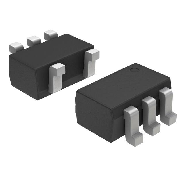
SC−88A / SOT−353 / SC−70
DF SUFFIX
CASE 419A
High Speed: tPD = 4.3 ns (Typ) at VCC = 5 V
Low Internal Power Dissipation: ICC = 1 mA (Max) at TA = 25°C
VX
M
G
Power Down Protection Provided on Inputs
Pin and Function Compatible with Other Standard Logic Families
Chip Complexity: FETs = 62; Equivalent Gates = 16
These Devices are Pb−Free, Halogen Free/BFR Free and are RoHS
Compliant
VX M G
G
1
= Device Code
= Date Code*
= Pb−Free Package
(Note: Microdot may be in either location)
*Date Code orientation and/or position may
vary depending upon manufacturing location.
PIN ASSIGNMENT
IN B
1
5
VCC
OVT
IN A
2
1
IN B
2
IN A
3
GND
4
OUT Y
5
VCC
FUNCTION TABLE
GND
3
4
Inputs
OUT Y
Figure 1. Pinout (Top View)
IN A
IN B
&
Output
A
B
Y
L
L
H
H
L
H
L
H
L
L
L
Z
OUT Y
Figure 2. Logic Symbol
ORDERING INFORMATION
See detailed ordering and shipping information in the package
dimensions section on page 4 of this data sheet.
© Semiconductor Components Industries, LLC, 2017
September, 2018 − Rev. 1
1
Publication Order Number:
MC74VHC1G09E/D
�MC74VHC1G09E
MAXIMUM RATINGS
Symbol
Characteristics
Value
Unit
VCC
DC Supply Voltage
−0.5 to +6.5
V
VIN
DC Input Voltage
−0.5 to +6.5
V
VOUT
DC Output Voltage
−0.5 to +6.5
V
IIK
Input Diode Current
−20
mA
IOK
Output Diode Current
+20
mA
IOUT
DC Output Current, per Pin
+25
mA
ICC
DC Supply Current, VCC and GND
+50
mA
PD
Power dissipation in still air
200
mW
qJA
Thermal resistance
333
°C/W
TL
Lead temperature, 1 mm from case for 10 s
260
°C
TJ
Junction temperature under bias
+150
°C
Tstg
Storage temperature
−65 to +150
°C
MSL
Moisture Sensitivity
Level 1
FR
Flammability Rating
VESD
ILatchup
Oxygen Index: 28 to 34
ESD Withstand Voltage
Latchup Performance
UL 94 V−0 @ 0.125 in
Human Body Model (Note 1)
Charged Device Model (Note 2)
4000
1000
V
Above VCC and Below GND at 125°C (Note 3)
±100
mA
Stresses exceeding those listed in the Maximum Ratings table may damage the device. If any of these limits are exceeded, device functionality
should not be assumed, damage may occur and reliability may be affected.
1. Tested to EIA/JESD22−A114−A
2. Tested to JESD22−C101−A
3. Tested to EIA/JESD78
RECOMMENDED OPERATING CONDITIONS
Symbol
Min
Max
Unit
VCC
DC Supply Voltage
2.0
5.5
V
VIN
DC Input Voltage
0.0
5.5
V
DC Output Voltage
0.0
7.0
V
TA
Operating Temperature Range
−55
+125
°C
tr, tf
Input Rise and Fall Time
0
0
10
5
ns/V
VOUT
Characteristics
VCC = 3.3 V ± 0.3 V
VCC = 5.0 V ± 0.5 V
Functional operation above the stresses listed in the Recommended Operating Ranges is not implied. Extended exposure to stresses beyond
the Recommended Operating Ranges limits may affect device reliability.
www.onsemi.com
2
�MC74VHC1G09E
DC ELECTRICAL CHARACTERISTICS
Test Conditions
Min
1.5
2.1
3.15
3.85
Symbol
Parameter
VIH
Minimum High−Level
Input Voltage
2.0
3.0
4.5
5.5
VIL
Maximum Low−Level
Input Voltage
2.0
3.0
4.5
5.5
VOL
Maximum Low−Level
Output Voltage
VIN = VIH or VIL
TA ≤ 85°C
TA = 25°C
VCC
(V)
Typ
Max
Min
−55 ≤ TA ≤ 125°C
Max
Min
1.5
2.1
3.15
3.85
0.0
0.0
0.0
Max
1.5
2.1
3.15
3.85
Unit
V
0.5
0.9
1.35
1.65
0.5
0.9
1.35
1.65
0.5
0.9
1.35
1.65
V
0.1
0.1
0.1
0.1
0.1
0.1
0.1
0.1
0.1
V
VIN = VIH or VIL
IOL = 50 mA
2.0
3.0
4.5
VIN = VIH or VIL
IOL = 4 mA
IOL = 8 mA
3.0
4.5
0.36
0.36
0.44
0.44
0.52
0.52
V
IIN
Maximum Input
Leakage Current
VIN = 5.5 V or GND
0 to
5.5
±0.1
±1.0
±1.0
mA
ICC
Maximum Quiescent
Supply Current
VIN = VCC or GND
5.5
1.0
20
40
mA
IOFF
Power Off−Output
Leakage Current
VOUT = 5.5 V
VIN = 5.5 V
0
0.25
2.5
5
mA
AC ELECTRICAL CHARACTERISTICS Input tr = tf = 3.0 ns
TA ≤ 85°C
TA = 25°C
Symbol
tPZL
tPLZ
CIN
Parameter
Maximum Output
Enable Time,
Input A or B to Y
Maximum Output
Disable Time
Min
Typ
Max
VCC = 3.3 ± 0.3 V CL = 15 pF
RL = 1000 W
CL = 50 pF
6.2
8.7
8.8
12.3
VCC = 5.0 ± 0.5 V CL = 15 pF
RL = 1000 W
CL = 50 pF
4.3
5.8
VCC = 3.3 ± 0.3 V CL = 50 pF
RL = 1000 W
VCC = 5.0 ± 0.5 V CL = 50 pF
RL = 1000 W
Test Conditions
Maximum Input Capacitance
Min
−55 ≤ TA ≤ 125°C
Max
Min
Max
Unit
10.5
14.0
12.5
16.5
ns
5.9
7.9
7.0
9.0
9.0
11.0
8.7
12.3
14.0
16.5
5.8
7.9
9.0
11.0
6.0
10
10
10
ns
pF
Typical @ 25°C, VCC = 5.0 V
CPD
18
Power Dissipation Capacitance (Note 4)
pF
4. CPD is defined as the value of the internal equivalent capacitance which is calculated from the operating current consumption without load.
Average operating current can be obtained by the equation: ICC(OPR) = CPD � VCC � fin + ICC. CPD is used to determine the no−load dynamic
power consumption; PD = CPD � VCC2 � fin + ICC � VCC.
www.onsemi.com
3
�MC74VHC1G09E
VCC
2 V to 5.5 V
OVT
A
VCC
A or B
RL
50%
GND
B
tPLZ
tPZL
HIGH
IMPEDANCE
50% VCC
Y
Figure 3. Output Voltage Mismatch Application
VOL +0.3 V
Figure 4. Switching Waveforms
VCC
RL
PULSE
GENERATOR
VCC
DUT
RT
CL
CL = 50 pF equivalent (Includes jig and probe capacitance)
RL = 1000 W or equivalent
RT = ZOUT of pulse generator (typically 50 W)
Figure 5. Test Circuit
VCC
VCC
MC74VHC1G09E
A
2.2 kW
B
B
A
1
VCC
5
MC74VHC1G09E
3.3 V
1.5 V
RLED
2
MC74VHC1G03
4
3
C
D
E = (A • B) + (C+D)
Figure 6. Complex Boolean Functions
220 W
A
GTL
B
Figure 7. LED Driver
Figure 8. GTL Driver
ORDERING INFORMATION
Device
MC74VHC1G09EDFT2G
Package
Shipping†
SC70−5 / SC−88A / SOT−353
(Pb−Free)
3000/Tape & Reel
†For information on tape and reel specifications, including part orientation and tape sizes, please refer to our Tape and Reel Packaging
Specifications Brochure, BRD8011/D.
www.onsemi.com
4
�MC74VHC1G09E
PACKAGE DIMENSIONS
SC−88A (SC−70−5/SOT−353)
CASE 419A−02
ISSUE L
A
G
5
4
NOTES:
1. DIMENSIONING AND TOLERANCING
PER ANSI Y14.5M, 1982.
2. CONTROLLING DIMENSION: INCH.
3. 419A−01 OBSOLETE. NEW STANDARD
419A−02.
4. DIMENSIONS A AND B DO NOT INCLUDE
MOLD FLASH, PROTRUSIONS, OR GATE
BURRS.
−B−
S
1
2
DIM
A
B
C
D
G
H
J
K
N
S
3
D 5 PL
0.2 (0.008)
M
B
M
N
INCHES
MIN
MAX
0.071
0.087
0.045
0.053
0.031
0.043
0.004
0.012
0.026 BSC
--0.004
0.004
0.010
0.004
0.012
0.008 REF
0.079
0.087
MILLIMETERS
MIN
MAX
1.80
2.20
1.15
1.35
0.80
1.10
0.10
0.30
0.65 BSC
--0.10
0.10
0.25
0.10
0.30
0.20 REF
2.00
2.20
J
C
K
H
SOLDERING FOOTPRINT*
0.50
0.0197
0.65
0.025
0.65
0.025
0.40
0.0157
1.9
0.0748
SCALE 20:1
mm Ǔ
ǒinches
*For additional information on our Pb−Free strategy and soldering
details, please download the ON Semiconductor Soldering and
Mounting Techniques Reference Manual, SOLDERRM/D.
ON Semiconductor and
are trademarks of Semiconductor Components Industries, LLC dba ON Semiconductor or its subsidiaries in the United States and/or other countries.
ON Semiconductor owns the rights to a number of patents, trademarks, copyrights, trade secrets, and other intellectual property. A listing of ON Semiconductor’s product/patent
coverage may be accessed at www.onsemi.com/site/pdf/Patent−Marking.pdf. ON Semiconductor reserves the right to make changes without further notice to any products herein.
ON Semiconductor makes no warranty, representation or guarantee regarding the suitability of its products for any particular purpose, nor does ON Semiconductor assume any liability
arising out of the application or use of any product or circuit, and specifically disclaims any and all liability, including without limitation special, consequential or incidental damages.
Buyer is responsible for its products and applications using ON Semiconductor products, including compliance with all laws, regulations and safety requirements or standards,
regardless of any support or applications information provided by ON Semiconductor. “Typical” parameters which may be provided in ON Semiconductor data sheets and/or
specifications can and do vary in different applications and actual performance may vary over time. All operating parameters, including “Typicals” must be validated for each customer
application by customer’s technical experts. ON Semiconductor does not convey any license under its patent rights nor the rights of others. ON Semiconductor products are not
designed, intended, or authorized for use as a critical component in life support systems or any FDA Class 3 medical devices or medical devices with a same or similar classification
in a foreign jurisdiction or any devices intended for implantation in the human body. Should Buyer purchase or use ON Semiconductor products for any such unintended or unauthorized
application, Buyer shall indemnify and hold ON Semiconductor and its officers, employees, subsidiaries, affiliates, and distributors harmless against all claims, costs, damages, and
expenses, and reasonable attorney fees arising out of, directly or indirectly, any claim of personal injury or death associated with such unintended or unauthorized use, even if such
claim alleges that ON Semiconductor was negligent regarding the design or manufacture of the part. ON Semiconductor is an Equal Opportunity/Affirmative Action Employer. This
literature is subject to all applicable copyright laws and is not for resale in any manner.
PUBLICATION ORDERING INFORMATION
LITERATURE FULFILLMENT:
Literature Distribution Center for ON Semiconductor
19521 E. 32nd Pkwy, Aurora, Colorado 80011 USA
Phone: 303−675−2175 or 800−344−3860 Toll Free USA/Canada
Fax: 303−675−2176 or 800−344−3867 Toll Free USA/Canada
Email: orderlit@onsemi.com
◊
N. American Technical Support: 800−282−9855 Toll Free
USA/Canada
Europe, Middle East and Africa Technical Support:
Phone: 421 33 790 2910
www.onsemi.com
5
ON Semiconductor Website: www.onsemi.com
Order Literature: http://www.onsemi.com/orderlit
For additional information, please contact your local
Sales Representative
MC74VHC1G09E/D
�