ON Semiconductor
Is Now
To learn more about onsemi™, please visit our website at
www.onsemi.com
onsemi and and other names, marks, and brands are registered and/or common law trademarks of Semiconductor Components Industries, LLC dba “onsemi” or its affiliates and/or
subsidiaries in the United States and/or other countries. onsemi owns the rights to a number of patents, trademarks, copyrights, trade secrets, and other intellectual property. A listing of onsemi
product/patent coverage may be accessed at www.onsemi.com/site/pdf/Patent-Marking.pdf. onsemi reserves the right to make changes at any time to any products or information herein, without
notice. The information herein is provided “as-is” and onsemi makes no warranty, representation or guarantee regarding the accuracy of the information, product features, availability, functionality,
or suitability of its products for any particular purpose, nor does onsemi assume any liability arising out of the application or use of any product or circuit, and specifically disclaims any and all
liability, including without limitation special, consequential or incidental damages. Buyer is responsible for its products and applications using onsemi products, including compliance with all laws,
regulations and safety requirements or standards, regardless of any support or applications information provided by onsemi. “Typical” parameters which may be provided in onsemi data sheets and/
or specifications can and do vary in different applications and actual performance may vary over time. All operating parameters, including “Typicals” must be validated for each customer application
by customer’s technical experts. onsemi does not convey any license under any of its intellectual property rights nor the rights of others. onsemi products are not designed, intended, or authorized
for use as a critical component in life support systems or any FDA Class 3 medical devices or medical devices with a same or similar classification in a foreign jurisdiction or any devices intended for
implantation in the human body. Should Buyer purchase or use onsemi products for any such unintended or unauthorized application, Buyer shall indemnify and hold onsemi and its officers, employees,
subsidiaries, affiliates, and distributors harmless against all claims, costs, damages, and expenses, and reasonable attorney fees arising out of, directly or indirectly, any claim of personal injury or death
associated with such unintended or unauthorized use, even if such claim alleges that onsemi was negligent regarding the design or manufacture of the part. onsemi is an Equal Opportunity/Affirmative
Action Employer. This literature is subject to all applicable copyright laws and is not for resale in any manner. Other names and brands may be claimed as the property of others.
�MC74VHC595
8-Bit Shift Register with
Output Storage Register
(3-State)
The MC74VHC595 is an advanced high speed 8−bit shift register
with an output storage register fabricated with silicon gate CMOS
technology.
It achieves high speed operation similar to equivalent Bipolar
Schottky TTL while maintaining CMOS low power dissipation.
The MC74VHC595 contains an 8−bit static shift register which
feeds an 8−bit storage register.
Shift operation is accomplished on the positive going transition of
the Shift Clock input (SCK). The output register is loaded with the
contents of the shift register on the positive going transition of the
Register Clock input (RCK). Since the RCK and SCK signals are
independent, parallel outputs can be held stable during the shift
operation. And, since the parallel outputs are 3−state, the VHC595 can
be directly connected to an 8−bit bus. This register can be used in
serial−to−parallel conversion, data receivers, etc.
The internal circuit is composed of three stages, including a buffer
output which provides high noise immunity and stable output. The
inputs tolerate voltages up to 7 V, allowing the interface of 5 V systems
to 3 V systems.
Features
•
•
•
•
•
•
•
•
•
•
•
•
High Speed: fmax = 185 MHz (Typ) at VCC = 5 V
Low Power Dissipation: ICC = 4 mA (Max) at TA = 25°C
High Noise Immunity: VNIH = VNIL = 28% VCC
Power Down Protection Provided on Inputs
Balanced Propagation Delays
Designed for 2 V to 5.5 V Operating Range
Low Noise: VOLP = 1.0 V (Max)
Pin and Function Compatible with Other Standard Logic Families
Latchup Performance Exceeds 300 mA
ESD Performance: HBM > 2000 V; Machine Model > 200 V
NLV Prefix for Automotive and Other Applications Requiring
Unique Site and Control Change Requirements; AEC−Q100
Qualified and PPAP Capable
These Devices are Pb−Free and are RoHS Compliant
www.onsemi.com
MARKING DIAGRAMS
16
9
VHC595G
AWLYWW
SOIC−16
D SUFFIX
CASE 751B
1
8
16
9
VHC
595
ALYWG
G
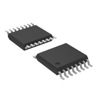
TSSOP−16
DT SUFFIX
CASE 948F
8
1
A
= Assembly Location
WL
= Wafer Lot
Y
= Year
W, WW = Work Week
G or G = Pb−Free Package
(Note: Microdot may be in either location)
PIN ASSIGNMENT
QB
1
16
VCC
QC
2
15
QA
QD
3
14
SI
QE
4
13
OE
QF
5
12
RCK
QG
6
11
SCK
QH
7
10
SCLR
GND
8
9
SQH
ORDERING INFORMATION
Device
Package
Shipping†
MC74VHC595DR2G
SOIC−16
(Pb−Free)
2500 Tape &
Reel
MC74VHC595DTR2G, TSSOP−16
NLV74VHC595DTR2G (Pb−Free)
2500 Tape &
Reel
†For information on tape and reel specifications,
including part orientation and tape sizes, please
refer to our Tape and Reel Packaging Specification
Brochure, BRD8011/D.
© Semiconductor Components Industries, LLC, 2015
February, 2015 − Rev. 6
1
Publication Order Number:
MC74VHC595/D
�MC74VHC595
LOGIC DIAGRAM
SERIAL
DATA
INPUT
SI
14
15
1
2
3
SHIFT
REGISTER
4
STORAGE
REGISTER
5
6
7
SCK
SCLR
RCK
OE
QA
QB
QC
PARALLEL
DATA
OUTPUTS
QD
QE
QF
QG
QH
11
9
10
SQH
12
13
IEC LOGIC SYMBOL
OE
RSK
SCLR
SCK
SI
13
12
10
EN3
C2
SRG8
R
11
14
C/1
1D
2D
3
15
1
2
3
4
5
6
2D
3
7
9
www.onsemi.com
2
QA
QB
QC
QD
QE
QF
QG
QH
SQH
SERIAL
DATA
OUTPUT
�MC74VHC595
EXPANDED LOGIC DIAGRAM
OE
RCK
�SI
13
12
14
D
D
Q
SRA
Q
15
QA
STRA
R
Q
D
D
SRB
Q
1
QB
STRB
R
Q
D
D
SRC
Q
2
QC
STRC
R
Q
D
D
SRD
Q
3
QD
STRD
PARALLEL
DATA
OUTPUTS
R
Q
D
D
SRE
Q
4
QE
STRE
R
Q
D
D
SRF
Q
5
QF
STRF
R
Q
D
D
SRG
Q
6
QG
STRG
R
Q
D
�SCK
11
D
SRH
Q
7
QH
STRH
R
SCLR
10
9
www.onsemi.com
3
SQH
�MC74VHC595
FUNCTION TABLE
Inputs
Resulting Function
Reset
(SCLR)
Serial
Input
(SI)
Shift
Clock
(SCK)
Reg
Clock
(RCK)
Output
Enable
(OE)
Shift
Register
Contents
Storage
Register
Contents
Serial
Output
(SQH)
Parallel
Outputs
(QA − QH)
Clear shift register
L
X
X
L, H, ↓
L
L
U
L
U
Shift data into shift
register
H
D
↑
L, H, ↓
L
D→SRA;
SRN→SRN+1
U
SRG→SRH
U
Registers remains
unchanged
H
X
L, H, ↓
X
L
U
**
U
**
Transfer shift register
contents to storage
register
H
X
L, H, ↓
↑
L
U
SRN³STRN
*
SRN
Storage register remains
unchanged
X
X
X
L, H, ↓
L
*
U
*
U
Enable parallel outputs
X
X
X
X
L
*
**
*
Enabled
Force outputs into high
impedance state
X
X
X
X
H
*
**
*
Z
Operation
SR = shift register contents
D = data (L, H) logic level
STR = storage register contents U = remains unchanged
↓ = High−to−Low
↑ = Low−to−High
* = depends on Reset and Shift Clock inputs
** = depends on Register Clock input
MAXIMUM RATINGS*
Symbol
Value
Unit
VCC
DC Supply Voltage
Parameter
– 0.5 to + 7.0
V
Vin
DC Input Voltage
– 0.5 to + 7.0
V
Vout
DC Output Voltage
– 0.5 to VCC + 0.5
V
IIK
Input Diode Current
− 20
mA
IOK
Output Diode Current
± 20
mA
Iout
DC Output Current, per Pin
± 25
mA
ICC
DC Supply Current, VCC and GND Pins
± 50
mA
PD
Power Dissipation in Still Air,
500
450
mW
Tstg
Storage Temperature
– 65 to + 150
_C
SOIC Packages†
TSSOP Package†
Stresses exceeding those listed in the Maximum Ratings table may damage the device. If any of
these limits are exceeded, device functionality should not be assumed, damage may occur and
reliability may be affected.
†Derating — SOIC Packages: – 7 mW/_C from 65_ to 125_C
TSSOP Package: − 6.1 mW/_C from 65_ to 125_C
RECOMMENDED OPERATING CONDITIONS
Symbol
Parameter
Min
Max
Unit
VCC
DC Supply Voltage
2.0
5.5
V
Vin
DC Input Voltage
0
5.5
V
Vout
DC Output Voltage
0
VCC
V
− 55
+ 125
_C
0
0
100
20
ns/V
TA
Operating Temperature, All Package Types
tr, tf
Input Rise and Fall Time
VCC = 3.3V ±0.3V
VCC =5.0V ±0.5V
Functional operation above the stresses listed in the Recommended Operating Ranges is not
implied. Extended exposure to stresses beyond the Recommended Operating Ranges limits may
affect device reliability.
www.onsemi.com
4
This device contains protection
circuitry to guard against damage
due to high static voltages or electric
fields. However, precautions must
be taken to avoid applications of any
voltage higher than maximum rated
voltages to this high−impedance circuit. For proper operation, Vin and
Vout should be constrained to the
range GND v (Vin or Vout) v VCC.
Unused inputs must always be
tied to an appropriate logic voltage
level (e.g., either GND or V CC ).
Unused outputs must be left open.
�MC74VHC595
The qJA of the package is equal to 1/Derating. Higher junction temperatures may affect the expected lifetime of the device per the table and
figure below.
47.9
100
178,700
20.4
110
79,600
9.4
120
37,000
4.2
130
17,800
2.0
140
8,900
1.0
TJ = 80 ° C
117.8
419,300
TJ = 90 ° C
1,032,200
90
TJ = 100 ° C
80
FAILURE RATE OF PLASTIC = CERAMIC
UNTIL INTERMETALLICS OCCUR
TJ = 110° C
Time, Years
TJ = 120° C
Time, Hours
TJ = 130 ° C
Junction
Temperature °C
NORMALIZED FAILURE RATE
DEVICE JUNCTION TEMPERATURE VERSUS
TIME TO 0.1% BOND FAILURES
1
1
10
100
1000
TIME, YEARS
Figure 1. Failure Rate vs. Time
Junction Temperature
DC ELECTRICAL CHARACTERISTICS
1.5
2.1
3.15
3.85
Parameter
VIH
Minimum High−Level
Input Voltage
2.0
3.0
4.5
5.5
VIL
Maximum Low−Level
Input Voltage
2.0
3.0
4.5
5.5
VOH
Minimum High−Level
Output Voltage
VIN = VIH or VIL
VOL
Maximum Low−Level
Output Voltage
VIN = VIH or VIL
Test Conditions
Min
Symbol
TA = ≤ 85°C
TA = 25°C
VCC
(V)
Typ
Max
Min
1.5
2.1
3.15
3.85
0.59
0.9
1.35
1.65
VIN = VIH or VIL
IOH = − 50 μA
2.0
3.0
4.5
1.9
2.9
4.4
VIN = VIH or VIL
IOH = −4 mA
IOH = −8 mA
3.0
4.5
2.58
3.94
VIN = VIH or VIL
IOL = 50 μA
2.0
3.0
4.5
VIN = VIH or VIL
IOL = 4 mA
IOL = 8 mA
Max
2.0
3.0
4.5
0.0
0.0
0.0
TA = ≤ 125°C
Min
Max
1.5
2.1
3.15
3.85
0.59
0.9
1.35
1.65
V
0.59
0.9
1.35
1.65
1.9
2.9
4.4
1.9
2.9
4.4
2.48
3.80
2.34
3.66
Unit
V
V
0.1
0.1
0.1
0.1
0.1
0.1
0.1
0.1
0.1
3.0
4.5
0.36
0.36
0.44
0.44
0.52
0.52
V
IIN
Maximum Input
Leakage Current
VIN = 5.5 V or GND
0 to
5.5
± 0.1
± 1.0
± 1.0
μA
ICC
Maximum Quiescent
Supply Current
VIN = VCC or GND
5.5
4.0
40.0
40.0
μA
IOZ
Three−State Output
Off−State Current
VIN = VIH or VIL
VOUT = VCC or
GND
5.5
± 0.25
± 2.5
± 2.5
μA
Product parametric performance is indicated in the Electrical Characteristics for the listed test conditions, unless otherwise noted. Product
performance may not be indicated by the Electrical Characteristics if operated under different conditions.
www.onsemi.com
5
�MC74VHC595
AC ELECTRICAL CHARACTERISTICS (Input tr = tf = 3.0ns)
TA = 25°C
Symbol
fmax
tPLH,
tPHL
tPHL
tPLH,
tPHL
tPZL,
tPZH
tPLZ,
tPHZ
Parameter
Min
Test Conditions
Typ
Max
TA = ≤ 85°C
TA = ≤ 125°C
Min
Min
Max
Max
Maximum Clock
Frequency (50%
Duty Cycle)
VCC = 3.3 ± 0.3 V
80
150
70
70
VCC = 5.0 ± 0.5 V
135
185
115
115
Propagation
Delay, SCK to
SQH
VCC = 3.3 ± 0.3 V
CL = 15pF
CL = 50pF
8.8
11.3
13.0
16.5
1.0
1.0
15.0
18.5
1.0
1.0
15.0
18.5
VCC = 5.0 ± 0.5 V
CL = 15pF
CL = 50pF
6.2
7.7
8.2
10.2
1.0
1.0
9.4
11.4
1.0
1.0
9.4
11.4
Propagation
Delay,
CPLR to SQH
VCC = 3.3 ± 0.3 V
CL = 15pF
CL = 50pF
8.4
10.9
12.8
16.3
1.0
1.0
13.7
17.2
1.0
1.0
13.7
17.2
VCC = 5.0 ± 0.5 V
CL = 15pF
CL = 50pF
5.9
7.4
8.0
10.0
1.0
1.0
9.1
11.1
1.0
1.0
9.1
11.1
Propagation
Delay, RCK to
QA−QH
VCC = 3.3 ± 0.3 V
CL = 15pF
CL = 50pF
7.7
10.2
11.9
15.4
1.0
1.0
13.5
17.0
1.0
1.0
13.5
17.0
VCC = 5.0 ± 0.5 V
CL = 15pF
CL = 50pF
5.4
6.9
7..4
9.4
1.0
1.0
8.5
10.5
1.0
1.0
8.5
10.5
Output Enable
Time,
OE to QA−QH
VCC = 3.3 ± 0.3 V
RL = 1 kW
CL = 15pF
CL = 50pF
7.5
9.0
11.5
15.0
1.0
1.0
13.5
17.0
1.0
1.0
13.5
17.0
VCC = 5.0 ± 0.5 V
RL = 1 kW
CL = 15pF
CL = 50pF
4.8
8.3
8.6
10.6
1.0
1.0
10.0
12.0
1.0
1.0
10.0
12.0
Output Disable
Time,
OE to QA−QH
VCC = 3.3 ± 0.3 V
RL = 1 kW
CL = 50pF
12.1
15.7
1.0
16.2
1.0
16.2
VCC = 5.0 ± 0.5 V
RL = 1 kW
CL = 50pF
7.6
10.3
1.0
11.0
1.0
11.0
10
CIN
Input Capacitance
4
COUT
Three−State
Output
Capacitance
(Output in
High−Impedance
State), QA−QH
6
Unit
MHz
ns
ns
ns
ns
ns
10
10
pF
10
10
pF
Typical @ 25°C, VCC = 5.0V
CPD
87
Power Dissipation Capacitance (Note 1)
pF
1. CPD is defined as the value of the internal equivalent capacitance which is calculated from the operating current consumption without load.
Average operating current can be obtained by the equation: ICC(OPR) = CPD � VCC � fin + ICC. CPD is used to determine the no−load dynamic
power consumption; PD = CPD � VCC2 � fin + ICC � VCC.
NOISE CHARACTERISTICS (Input tr = tf = 3.0ns, CL = 50pF, VCC = 5.0V)
TA = 25°C
Symbol
Characteristic
Typ
Max
Unit
VOLP
Quiet Output Maximum Dynamic VOL
0.8
1.0
V
VOLV
Quiet Output Minimum Dynamic VOL
− 0.8
− 1.0
V
VIHD
Minimum High Level Dynamic Input Voltage
3.5
V
VILD
Maximum Low Level Dynamic Input Voltage
1.5
V
www.onsemi.com
6
�MC74VHC595
TIMING REQUIREMENTS (Input tr = tf = 3.0ns)
Symbol
tsu
Parameter
TA = − 40 to
85°C
TA = − 55 to
125°C
Limit
Limit
Limit
Unit
TA = 25_C
VCC
V
Typ
Setup Time, SI to SCK
3.3
5.0
3.5
3.0
3.5
3.0
3.5
3.0
ns
tsu(H)
Setup Time, SCK to RCK
3.3
5.0
8.0
5.0
8.5
5.0
8.5
5.0
ns
tsu(L)
Setup Time, SCLR to RCK
3.3
5.0
8.0
5.0
9.0
5.0
9.0
5.0
ns
Hold Time, SI to SCK
3.3
5.0
1.5
2.0
1.5
2.0
1.5
2.0
ns
th(L)
Hold Time, SCLR to RCK
3.3
5.0
0
0
0
0
1.0
1.0
ns
trec
Recovery Time, SCLR to SCK
3.3
5.0
3.0
2.5
3.0
2.5
3.0
2.5
ns
tw
Pulse Width, SCK or RCK
3.3
5.0
5.0
5.0
5.0
5.0
5.0
5.0
ns
Pulse Width, SCLR
3.3
5.0
5.0
5.0
5.0
5.0
5.0
5.0
ns
th
tw(L)
www.onsemi.com
7
�MC74VHC595
SWITCHING WAVEFORMS
tw
VCC
VCC
GND
GND
tw
tPHL
1/fmax
tPLH
50%
SCLR
50%
SCK
50% VCC
SQH
tPHL
trec
SQH
VCC
50% VCC
50%
SCK
GND
Figure 2.
Figure 3.
VCC
RCK
VCC
50%
50%
OE
GND
GND
tPLH
tPZL
tPHL
tPLZ
50% VCC
QA-QH
tPZH
QA-QH
50% VCC
HIGH
IMPEDANCE
QA-QH
VOL +0.3V
tPHZ
VOH -0.3V
50% VCC
Figure 4.
HIGH
IMPEDANCE
Figure 5.
VCC
SCLR
50%
VCC
GND
VALID
50%
SCK
VCC
GND
50%
SI
tsu(H)
GND
tsu
th
VCC
GND
50%
SCK or RCK
VCC
50%
RCK
tw
GND
Figure 6.
Figure 7.
TEST CIRCUITS
TEST POINT
TEST POINT
OUTPUT
DEVICE
UNDER
TEST
OUTPUT
DEVICE
UNDER
TEST
CL*
*Includes all probe and jig capacitance
1 kΩ
CL*
CONNECT TO VCC WHEN
TESTING tPLZ AND tPZL.
CONNECT TO GND WHEN
TESTING tPHZ AND tPZH.
*Includes all probe and jig capacitance
Figure 8.
Figure 9.
www.onsemi.com
8
�MC74VHC595
TIMING DIAGRAM
SCK
�SI
SCLR
RCK
OE
QA
QB
QC
QD
QE
QF
QG
QH
SQH
NOTE:
output is in a high−impedance state.
INPUT EQUIVALENT CIRCUIT
INPUT
www.onsemi.com
9
�MC74VHC595
PACKAGE DIMENSIONS
TSSOP−16
CASE 948F
ISSUE B
16X K REF
0.10 (0.004)
0.15 (0.006) T U
T U
M
S
V
S
S
K
ÉÉÉ
ÇÇÇ
ÇÇÇ
ÉÉÉ
ÇÇÇ
K1
2X
L/2
16
9
J1
B
−U−
L
SECTION N−N
J
PIN 1
IDENT.
N
0.25 (0.010)
8
1
M
0.15 (0.006) T U
S
A
−V−
NOTES:
1. DIMENSIONING AND TOLERANCING PER
ANSI Y14.5M, 1982.
2. CONTROLLING DIMENSION: MILLIMETER.
3. DIMENSION A DOES NOT INCLUDE MOLD
FLASH. PROTRUSIONS OR GATE BURRS.
MOLD FLASH OR GATE BURRS SHALL NOT
EXCEED 0.15 (0.006) PER SIDE.
4. DIMENSION B DOES NOT INCLUDE
INTERLEAD FLASH OR PROTRUSION.
INTERLEAD FLASH OR PROTRUSION SHALL
NOT EXCEED 0.25 (0.010) PER SIDE.
5. DIMENSION K DOES NOT INCLUDE
DAMBAR PROTRUSION. ALLOWABLE
DAMBAR PROTRUSION SHALL BE 0.08
(0.003) TOTAL IN EXCESS OF THE K
DIMENSION AT MAXIMUM MATERIAL
CONDITION.
6. TERMINAL NUMBERS ARE SHOWN FOR
REFERENCE ONLY.
7. DIMENSION A AND B ARE TO BE
DETERMINED AT DATUM PLANE −W−.
N
F
DETAIL E
−W−
C
0.10 (0.004)
−T− SEATING
PLANE
H
D
DETAIL E
G
DIM
A
B
C
D
F
G
H
J
J1
K
K1
L
M
SOLDERING FOOTPRINT*
7.06
1
0.65
PITCH
16X
0.36
16X
1.26
DIMENSIONS: MILLIMETERS
*For additional information on our Pb−Free strategy and soldering
details, please download the ON Semiconductor Soldering and
Mounting Techniques Reference Manual, SOLDERRM/D.
www.onsemi.com
10
MILLIMETERS
MIN
MAX
4.90
5.10
4.30
4.50
−−−
1.20
0.05
0.15
0.50
0.75
0.65 BSC
0.18
0.28
0.09
0.20
0.09
0.16
0.19
0.30
0.19
0.25
6.40 BSC
0_
8_
INCHES
MIN
MAX
0.193 0.200
0.169 0.177
−−− 0.047
0.002 0.006
0.020 0.030
0.026 BSC
0.007
0.011
0.004 0.008
0.004 0.006
0.007 0.012
0.007 0.010
0.252 BSC
0_
8_
�MC74VHC595
PACKAGE DIMENSIONS
SOIC−16
CASE 751B−05
ISSUE K
−A−
16
9
1
8
−B−
P
NOTES:
1. DIMENSIONING AND TOLERANCING PER ANSI
Y14.5M, 1982.
2. CONTROLLING DIMENSION: MILLIMETER.
3. DIMENSIONS A AND B DO NOT INCLUDE MOLD
PROTRUSION.
4. MAXIMUM MOLD PROTRUSION 0.15 (0.006) PER SIDE.
5. DIMENSION D DOES NOT INCLUDE DAMBAR
PROTRUSION. ALLOWABLE DAMBAR PROTRUSION
SHALL BE 0.127 (0.005) TOTAL IN EXCESS OF THE D
DIMENSION AT MAXIMUM MATERIAL CONDITION.
8 PL
0.25 (0.010)
B
M
S
DIM
A
B
C
D
F
G
J
K
M
P
R
G
R
K
F
X 45 _
C
−T−
SEATING
PLANE
J
M
D
MILLIMETERS
MIN
MAX
9.80
10.00
3.80
4.00
1.35
1.75
0.35
0.49
0.40
1.25
1.27 BSC
0.19
0.25
0.10
0.25
0_
7_
5.80
6.20
0.25
0.50
INCHES
MIN
MAX
0.386
0.393
0.150
0.157
0.054
0.068
0.014
0.019
0.016
0.049
0.050 BSC
0.008
0.009
0.004
0.009
0_
7_
0.229
0.244
0.010
0.019
16 PL
0.25 (0.010)
M
T B
S
A
S
SOLDERING FOOTPRINT*
8X
6.40
16X
1
1.12
16
16X
0.58
1.27
PITCH
8
9
DIMENSIONS: MILLIMETERS
*For additional information on our Pb−Free strategy and soldering
details, please download the ON Semiconductor Soldering and
Mounting Techniques Reference Manual, SOLDERRM/D.
ON Semiconductor and the
are registered trademarks of Semiconductor Components Industries, LLC (SCILLC) or its subsidiaries in the United States and/or other countries.
SCILLC owns the rights to a number of patents, trademarks, copyrights, trade secrets, and other intellectual property. A listing of SCILLC’s product/patent coverage may be accessed
at www.onsemi.com/site/pdf/Patent−Marking.pdf. SCILLC reserves the right to make changes without further notice to any products herein. SCILLC makes no warranty, representation
or guarantee regarding the suitability of its products for any particular purpose, nor does SCILLC assume any liability arising out of the application or use of any product or circuit, and
specifically disclaims any and all liability, including without limitation special, consequential or incidental damages. “Typical” parameters which may be provided in SCILLC data sheets
and/or specifications can and do vary in different applications and actual performance may vary over time. All operating parameters, including “Typicals” must be validated for each
customer application by customer’s technical experts. SCILLC does not convey any license under its patent rights nor the rights of others. SCILLC products are not designed, intended,
or authorized for use as components in systems intended for surgical implant into the body, or other applications intended to support or sustain life, or for any other application in which
the failure of the SCILLC product could create a situation where personal injury or death may occur. Should Buyer purchase or use SCILLC products for any such unintended or
unauthorized application, Buyer shall indemnify and hold SCILLC and its officers, employees, subsidiaries, affiliates, and distributors harmless against all claims, costs, damages, and
expenses, and reasonable attorney fees arising out of, directly or indirectly, any claim of personal injury or death associated with such unintended or unauthorized use, even if such claim
alleges that SCILLC was negligent regarding the design or manufacture of the part. SCILLC is an Equal Opportunity/Affirmative Action Employer. This literature is subject to all applicable
copyright laws and is not for resale in any manner.
PUBLICATION ORDERING INFORMATION
LITERATURE FULFILLMENT:
Literature Distribution Center for ON Semiconductor
P.O. Box 5163, Denver, Colorado 80217 USA
Phone: 303−675−2175 or 800−344−3860 Toll Free USA/Canada
Fax: 303−675−2176 or 800−344−3867 Toll Free USA/Canada
Email: orderlit@onsemi.com
N. American Technical Support: 800−282−9855 Toll Free
USA/Canada
Europe, Middle East and Africa Technical Support:
Phone: 421 33 790 2910
Japan Customer Focus Center
Phone: 81−3−5817−1050
www.onsemi.com
11
ON Semiconductor Website: www.onsemi.com
Order Literature: http://www.onsemi.com/orderlit
For additional information, please contact your local
Sales Representative
MC74VHC595/D
�