Negative Voltage Regulators
100 mA
MC79L00A Series
The MC79L00A Series negative voltage regulators are
inexpensive, easy−to−use devices suitable for numerous applications
requiring up to 100 mA. Like the higher powered MC7900 Series
negative regulators, this series features thermal shutdown and current
limiting, making them remarkably rugged. In most applications, no
external components are required for operation.
The MC79L00A devices are useful for on−card regulation or any
other application where a regulated negative voltage at a modest
current level is needed. These regulators offer substantial advantage
over the common resistor/Zener diode approach.
www.onsemi.com
THREE−TERMINAL LOW
CURRENT NEGATIVE FIXED
VOLTAGE REGULATORS
MARKING
DIAGRAMS
Features
•
•
•
•
•
•
No External Components Required
Internal Short Circuit Current Limiting
Internal Thermal Overload Protection
Low Cost
Complementary Positive Regulators Offered (MC78L00 Series)
Pb−Free Packages are Available
Pin 1. Vout
2. Vin
3. Vin
4. NC
5. GND
6. Vin
7. Vin
8. NC
8
1
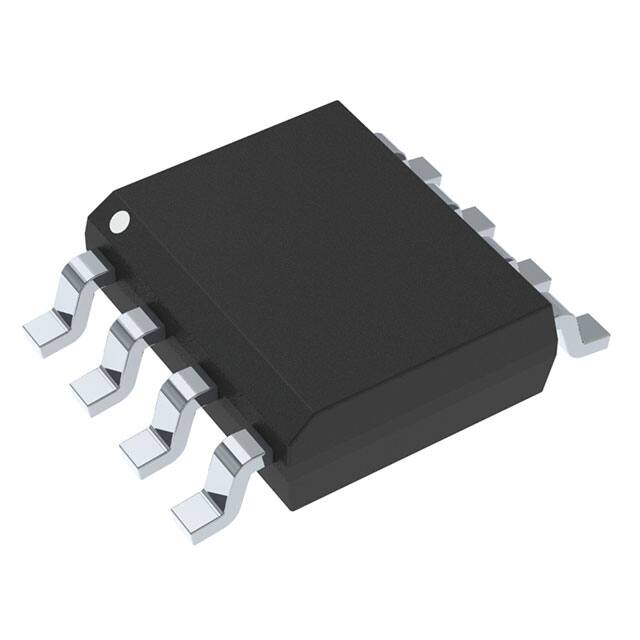
SOIC−8
D SUFFIX
CASE 751
R1
R8
R6
Q10
Q5
R9
Q4
1
12
3
STRAIGHT LEAD
R17
R7
Q8
Q1
R16
R4
1
2
3
BENT LEAD
Pin 1. Ground
2. Input
3. Output
Q14
Q9
9Lxxx
ALYWy
G
TO−92
P SUFFIX
CASE 29−10
GND
R
5
R18
8
Output
MC79L
xxxxx
ALYW
Q12
R2
Z1
R3
C
Q7
Q6
R10
Q13
Q2
R11
Q11
R14
R15
Input
*�Automotive temperature range selections are available with special test conditions
and additional tests in 5, 12 and 15 V devices. Contact your local ON Semiconductor
sales office for information.
xxx
A
L
Y
W
y
= Specific Device Code
= Assembly Location
= Wafer Lot
= Year
= Work Week
= B or C
Figure 1. Representative Schematic Diagram
ORDERING INFORMATION
See detailed ordering and shipping information in the package
dimensions section on page 7 of this data sheet.
© Semiconductor Components Industries, LLC, 1994
April, 2021 − Rev. 11
1
Publication Order Number:
MC79L00/D
�MC79L00A Series
MAXIMUM RATINGS (TA = +25°C, unless otherwise noted.)
Symbol
Value
Unit
VI
−30
−35
−40
Vdc
Power Dissipation
Case 29 (TO−92 Type)
TA = 25°C
Thermal Resistance, Junction−to−Ambient
Thermal Resistance, Junction−to−Case
PD
RqJA
RqJC
Internally Limited
160
83
W
°C/W
°C/W
Case 751 (SOIC−8 Type) (Note 1)
TA = 25°C
Thermal Resistance, Junction−to−Ambient
Thermal Resistance, Junction−to−Case
PD
RqJA
RqJC
Internally Limited
180
45
W
°C/W
°C/W
Tstg
−65 to +150
°C
TJ
+150
°C
Rating
Input Voltage
(−5 V)
(−12, −15, −18 V)
(−24 V)
Storage Temperature Range
Junction Temperature
Stresses exceeding those listed in the Maximum Ratings table may damage the device. If any of these limits are exceeded, device functionality
should not be assumed, damage may occur and reliability may be affected.
1. SOIC−8 Junction−to−Ambient Thermal Resistance is for minimum recommended pad size. Refer to Figure 9 for Thermal Resistance variation
versus pad size.
*This device series contains ESD protection and exceeds the following tests:
Human Body Model 2000 V per MIL_STD_883, Method 3015
Machine Model Method 200 V.
ELECTRICAL CHARACTERISTICS (VI = −10 V, IO = 40 mA, CI = 0.33 mF, CO = 0.1 mF, −40°C < TJ +125°C (for MC79LXXAB),
0°C < TJ < +125°C (for MC79LXXAC)).
MC79L05AC, AB
Characteristics
Symbol
Min
Typ
Max
Unit
VO
−4.8
−5.0
−5.2
Vdc
−
−
−
−
150
100
−
−
−
−
60
30
−4.75
−4.75
−
−
−5.25
−5.25
−
−
−
−
6.0
5.5
−
−
−
−
1.5
0.1
Output Voltage (TJ = +25°C)
Input Regulation (TJ = +25°C)
−7.0 Vdc ≥ VI ≥ −20 Vdc
−8.0 Vdc ≥ VI ≥ −20 Vdc
Regline
Load Regulation
TJ = +25°C, 1.0 mA ≤ IO ≤ 100 mA
1.0 mA ≤ IO ≤ 40 mA
Regload
mV
mV
Output Voltage
−7.0 Vdc ≥ VI ≥ −20 Vdc, 1.0 mA ≤ IO ≤ 40 mA
VI = −10 Vdc, 1.0 mA ≤ IO ≤ 70 mA
VO
Input Bias Current
(TJ = +25°C)
(TJ = +125°C)
IIB
Input Bias Current Change
−8.0 Vdc ≥ VI ≥ −20 Vdc
1.0 mA ≤ IO ≤ 40 mA
IIB
Output Noise Voltage (TA = +25°C, 10 Hz ≤ f ≤ 100 kHz)
Vn
−
40
−
mV
Ripple Rejection (−8.0 ≥ VI ≥ −18 Vdc, f = 120 Hz, TJ = +25°C)
RR
41
49
−
dB
|VI−VO|
−
1.7
−
Vdc
Dropout Voltage (IO = 40 mA, TJ = +25°C)
Vdc
mA
mA
Product parametric performance is indicated in the Electrical Characteristics for the listed test conditions, unless otherwise noted. Product
performance may not be indicated by the Electrical Characteristics if operated under different conditions.
www.onsemi.com
2
�MC79L00A Series
ELECTRICAL CHARACTERISTICS (VI = −19 V, IO = 40 mA, CI = 0.33 mF, CO = 0.1 mF, −40°C < TJ +125°C (for MC79LXXAB),
0°C < TJ < +125°C (for MC79LXXAC)).
MC79L12AC, AB
Characteristics
Symbol
Min
Typ
Max
Unit
VO
−11.5
−12
−12.5
Vdc
−
−
−
−
250
200
−
−
−
−
Output Voltage (TJ = +25°C)
Input Regulation (TJ = +25°C)
−14.5 Vdc ≥ VI ≥ −27 Vdc
−16 Vdc ≥ VI ≥ −27 Vdc
Regline
Load Regulation
TJ = +25°C, 1.0 mA ≤ IO ≤ 100 mA
1.0 mA ≤ IO ≤ 40 mA
Regload
Output Voltage
−14.5 Vdc ≥ VI ≥ −27 Vdc, 1.0 mA ≤ IO ≤ 40 mA
VI = −19 Vdc, 1.0 mA ≤ IO ≤ 70 mA
VO
Input Bias Current
(TJ = +25°C)
(TJ = +125°C)
IIB
Input Bias Current Change
−16 Vdc ≥ VI ≥ −27 Vdc
1.0 mA ≤ IO ≤ 40 mA
IIB
Output Noise Voltage (TA = +25°C, 10 Hz ≤ f ≤ 100 kHz)
Ripple Rejection (−15 ≤ VI ≤ −25 Vdc, f = 120 Hz, TJ = +25°C)
Dropout Voltage (IO = 40 mA, TJ = +25°C)
−11.4
−11.4
−
−
−
−
−
−
−
−
−
−
Vn
−
RR
|VI−VO|
mV
100
50
mV
−12.6
−12.6
Vdc
6.5
6.0
mA
1.5
0.2
mA
80
−
mV
37
42
−
dB
−
1.7
−
Vdc
Product parametric performance is indicated in the Electrical Characteristics for the listed test conditions, unless otherwise noted. Product
performance may not be indicated by the Electrical Characteristics if operated under different conditions.
ELECTRICAL CHARACTERISTICS (VI = −23 V, IO = 40 mA, CI = 0.33 mF, CO = 0.1 mF, −40°C < TJ +125°C (for MC79LXXAB),
0°C < TJ < +125°C (for MC79LXXAC)).
MC79L15AC, AB
Characteristics
Symbol
Min
Typ
Max
Unit
VO
−14.4
−15
−15.6
Vdc
−
−
−
−
300
250
−
−
−
−
150
75
−14.25
−14.25
−
−
−15.75
−15.75
−
−
−
−
6.5
6.0
−
−
−
−
1.5
0.1
Output Voltage (TJ = +25°C)
Input Regulation (TJ = +25°C)
−17.5 Vdc ≥ VI ≥ −30 Vdc
−20 Vdc ≥ VI ≥ −30 Vdc
Regline
Load Regulation
TJ = +25°C, 1.0 mA ≤ IO ≤ 100 mA
1.0 mA ≤ IO ≤ 40 mA
Regload
Output Voltage
−17.5 Vdc ≥ VI ≥ −Vdc, 1.0 mA ≤ IO ≤ 40 mA
VI = −23 Vdc, 1.0 mA ≤ IO ≤ 70 mA
VO
Input Bias Current
(TJ = +25°C)
(TJ = +125°C)
IIB
mV
mV
Vdc
mA
Input Bias Current Change
−20 Vdc ≥ VI ≥ −30 Vdc
1.0 mA ≤ IO ≤ 40 mA
DIIB
Output Noise Voltage (TA = +25°C, 10 Hz ≤ f ≤ 100 kHz)
VN
−
90
−
mV
Ripple Rejection (−18.5 ≤ VI ≤ −28.5 Vdc, f = 120 Hz)
RR
34
39
−
dB
|VI−VO|
−
1.7
−
Vdc
Dropout Voltage IO = 40 mA, TJ = +25°C
mA
Product parametric performance is indicated in the Electrical Characteristics for the listed test conditions, unless otherwise noted. Product
performance may not be indicated by the Electrical Characteristics if operated under different conditions.
www.onsemi.com
3
�MC79L00A Series
ELECTRICAL CHARACTERISTICS (VI = −27 V, IO = 40 mA, CI = 0.33 mF, CO = 0.1 mF, −40°C < TJ +125°C (for MC79LXXAB),
0°C < TJ < +125°C (for MC79LXXAC), unless otherwise noted).
MC79L18AC
Characteristics
Symbol
Min
Typ
Max
Unit
VO
−17.3
−18
−18.7
Vdc
−
−
−
−
−
−
−
−
325
−
−
275
−
−
−
−
170
85
−17.1
−
−17.1
−
−
−
−18.9
−
−18.9
−
−
−
−
6.5
6.0
−
−
−
−
−
−
1.5
−
0.1
Output Voltage (TJ = +25°C)
Input Regulation (TJ = +25°C)
−20.7 Vdc ≥ VI ≥ −33 Vdc
−21.4 Vdc ≥ VI ≥ −33 Vdc
−22 Vdc ≥ VI ≥ −33 Vdc
−21 Vdc ≥ VI ≥ −33 Vdc
Regline
Load Regulation
TJ = +25°C, 1.0 mA ≤ IO ≤ 100 mA
1.0 mA ≤ IO ≤ 40 mA
Regload
mV
mV
Output Voltage
−20.7 Vdc ≥ VI ≥ −33 Vdc, 1.0 mA ≤ IO ≤ 40 mA
−21.4 Vdc ≥ VI ≥ −33 Vdc, 1.0 mA ≤ IO ≤ 40 mA
VI = −27 Vdc, 1.0 mA ≤ IO ≤ 70 mA
VO
Input Bias Current
(TJ = +25°C)
(TJ = +125°C)
IIB
Input Bias Current Change
−21 Vdc ≥ VI ≥ −33 Vdc
−27 Vdc ≥ VI ≥ −33 Vdc
1.0 mA ≤ IO ≤ 40 mA
IIB
Output Noise Voltage (TA = +25°C, 10 Hz ≤ f ≤ 100 kHz)
Vn
−
150
−
mV
Ripple Rejection (−23 ≤ VI ≤ −33 Vdc, f = 120 Hz, TJ = +25°C)
RR
33
48
−
dB
|VI−VO|
−
1.7
−
Vdc
Dropout Voltage IO = 40 mA, TJ = +25°C
Vdc
mA
mA
Product parametric performance is indicated in the Electrical Characteristics for the listed test conditions, unless otherwise noted. Product
performance may not be indicated by the Electrical Characteristics if operated under different conditions.
ELECTRICAL CHARACTERISTICS (VI = −33 V, IO = 40 mA, CI = 0.33 mF, CO = 0.1 mF, −40°C < TJ +125°C (for MC79LXXAB),
0°C < TJ < +125°C (for MC79LXXAC), unless otherwise noted).
MC79L24AC
Characteristics
Symbol
Min
Typ
Max
Unit
VO
−23
−24
−25
Vdc
−
−
−
−
−
−
350
−
300
−
−
−
−
200
100
−22.8
−
−22.8
−
−
−
−25.2
−
−25.2
−
−
−
−
6.5
6.0
−
−
−
−
1.5
0.1
Output Voltage (TJ = +25°C)
Input Regulation (TJ = +25°C)
−27 Vdc ≥ VI ≥ −38 Vdc
−27.5 Vdc ≥ VI ≥ −38 Vdc
−28 Vdc ≥ VI ≥ −38 Vdc
Regline
Load Regulation
TJ = +25°C, 1.0 mA ≤ IO ≤ 100 mA
1.0 mA ≤ IO ≤ 40 mA
Regload
Output Voltage
−27 Vdc ≥ VI ≥ −38 V, 1.0 mA ≤ IO ≤ 40 mA
−28 Vdc ≥ VI ≥ −38 Vdc, 1.0 mA ≤ IO ≤ 40 mA
VI = −33 Vdc, 1.0 mA ≤ IO ≤ 70 mA
VO
Input Bias Current
(TJ = +25°C)
(TJ = +125°C)
IIB
Input Bias Current Change
−28 Vdc ≥ VI ≥ −38 Vdc
1.0 mA ≤ IO ≤ 40 mA
DIIB
mV
mV
Vdc
mA
mA
Output Noise Voltage (TA = +25°C, 10 Hz ≤ f ≤ 100 kHz)
Vn
−
200
−
mV
Ripple Rejection (−29 ≤ VI ≤ −35 Vdc, f = 120 Hz, TJ = +25°C)
RR
31
47
−
dB
|VI−VO|
−
1.7
−
Vdc
Dropout Voltage IO = 40 mA, TJ = +25°C
Product parametric performance is indicated in the Electrical Characteristics for the listed test conditions, unless otherwise noted. Product
performance may not be indicated by the Electrical Characteristics if operated under different conditions.
www.onsemi.com
4
�MC79L00A Series
APPLICATIONS INFORMATION
Design Considerations
high−frequency characteristics to insure stable operation
under all load conditions. A 0.33 mF or larger tantalum,
mylar, or other capacitor having low internal impedance at
high frequencies should be chosen. The bypass capacitor
should be mounted with the shortest possible leads directly
across the regulator’s input terminals. Normally good
construction techniques should be used to minimize ground
loops and lead resistance drops since the regulator has no
external sense lead. Bypassing the output is also
recommended.
The MC79L00A Series of fixed voltage regulators are
designed with Thermal Overload Protections that shuts
down the circuit when subjected to an excessive power
overload condition, Internal Short Circuit Protection that
limits the maximum current the circuit will pass.
In many low current applications, compensation
capacitors are not required. However, it is recommended
that the regulator input be bypassed with a capacitor if the
regulator is connected to the power supply filter with long
wire length, or if the output load capacitance is large. An
input bypass capacitor should be selected to provide good
Input
+Vin
MC78LXX
+VO
CI*
0.33mF
0.1mF
0.33mF
MC79LXX
Output
CO**
0.1mF
0.1mF
-Vin
MC79LXX
A common ground is required between the input and the output
voltages. The input voltage must remain typically 2.0 V above
the output voltage even during the low point on the ripple voltage.
-VO
0.33mF
�* CI is required if regulator is located an appreciable
�* distance from the power supply filter
** CO improves stability and transient response.
Figure 2. Positive and Negative Regulator
Figure 3. Standard Application
www.onsemi.com
5
�MC79L00A Series
TYPICAL CHARACTERISTICS
(TA = +25°C, unless otherwise noted.)
MC79L05C
VO = -5.0 V
TJ = 25°C
6.0
IO = 1.0 mA
4.0
IO = 100 mA
2.0
IO = 40 mA
0
0
-2.0
-4.0
-6.0
Vin, INPUT VOLTAGE (V)
-0.8
-2.5
V I -V O , INPUT/OUTPUT DIFFERENTIAL
VOLTAGE (V)
-2.0
IO = 70 mA
IO = 40 mA
-1.5
IO = 1.0 mA
-1.0
Dropout of Regulation is
defined when
DVO = 2% of VO
-0.5
0
-10
0
25
Figure 4. Dropout Characteristics
I IB , INPUT BIAS CURRENT (mA)
5.0
4.0
3.8
3.6
3.4
MC79L05C
Vin = -10 V
VO = -5.0 V
IO = 40 mA
3.2
3.0
0
0
25
50
75
100
TA, AMBIENT TEMPERATURE (°C)
4.0
3.0
2.0
1.0
0
125
MC79L05C
VO = -5.0 V
IO = 40 mA
0
-5.0
Figure 6. Input Bias Current versus
Ambient Temperature
-10
-15
-20
-25
-30
Vin, INPUT VOLTAGE (V)
-35
170
3.2
RθJA , THERMAL RESISTANCE
JUNCTION-TO-AIR (°C/W)
150
2.8
PD(max) for TA = +50°C
130
1,000
No Heatsink
100
RqJA = 200°C/W
PD(max) to 25°C = 625 mW
10
25
50
75
100
125
TA, AMBIENT TEMPERATURE (°C)
-40
Figure 7. Input Bias Current versus
Input Voltage
10,000
P D , POWER DISSIPATION (mW)
125
Figure 5. Dropout Voltage versus
Junction Temperature
4.2
I IB , INPUT BIAS CURRENT (mA)
50
75
100
TJ, JUNCTION TEMPERATURE (°C)
2.4
ÎÎÎ
ÎÎÎ
ÎÎÎ
ÎÎÎ
ÎÎÎ
ÎÎÎ
110
Graph represents symmetrical layout
90
L
70
L
1.6
1.2
3.0 mm
50
0.8
RqJA
30
0
150
2.0 oz.
Copper
2.0
10
20
30
L, LENGTH OF COPPER (mm)
40
0.4
50
Figure 9. SOP−8 Thermal Resistance and Maximum
Power Dissipation versus P.C.B. Copper Length
Figure 8. Maximum Average Power Dissipation
versus Ambient Temperature (TO−92)
www.onsemi.com
6
PD, MAXIMUM POWER DISSIPATION (W)
VO, OUTPUT VOLTAGE (V)
8.0
�MC79L00A Series
ORDERING INFORMATION
Nominal
Voltage
Operating Temperature
Range
Package
Shipping†
−5.0 V
TJ = −40° to +125°C
SOIC−8
(Pb−Free)
98 Units / Rail
MC79L05ABDR2G
SOIC−8
(Pb−Free)
2500 / Tape & Reel
MC79L05ABPG
TO−92
(Pb−Free)
2000 Units / Bag
MC79L05ABPRAG
TO−92
(Pb−Free)
2000 / Tape & Reel
SOIC−8
(Pb−Free)
98 Units / Rail
MC79L05ACDR2G
SOIC−8
(Pb−Free)
2500 / Tape & Reel
MC79L05ACPG
TO−92
(Pb−Free)
2000 Units / Bag
MC79L05ACPRAG
TO−92
(Pb−Free)
2000 / Tape & Reel
MC79L05ACPRMG
TO−92
(Pb−Free)
2000 / Tape & Ammo Box
MC79L05ACPRPG
TO−92
(Pb−Free)
2000 / Tape & Ammo Box
SOIC−8
(Pb−Free)
98 Units / Rail
MC79L12ABDR2G
SOIC−8
(Pb−Free)
2500 / Tape & Reel
MC79L12ABPG
TO−92
(Pb−Free)
2000 Units / Bag
MC79L12ABPRAG
TO−92
(Pb−Free)
2000 / Tape & Reel
SOIC−8
(Pb−Free)
98 Units / Rail
MC79L12ACDR2G
SOIC−8
(Pb−Free)
2500 / Tape & Reel
MC79L12ACPG
TO−92
(Pb−Free)
2000 Units / Bag
MC79L12ACPRAG
TO−92
(Pb−Free)
2000 / Tape & Reel
MC79L12ACPRPG
TO−92
(Pb−Free)
2000 / Tape & Ammo Box
Device
MC79L05ABDG
MC79L05ACDG
MC79L12ABDG
MC79L12ACDG
TJ = 0° to +125°C
−12 V
−12 V
TJ = −40° to +125°C
TJ = 0° to +125°C
www.onsemi.com
7
�MC79L00A Series
ORDERING INFORMATION (continued)
Nominal
Voltage
Operating Temperature
Range
Package
Shipping†
−15 V
TJ = −40° to +125°C
SOIC−8
(Pb−Free)
98 Units / Rail
MC79L15ABDR2G
SOIC−8
(Pb−Free)
2500 / Tape & Reel
MC79L15ABPG
TO−92
(Pb−Free)
2000 Units / Bag
MC79L15ABPRPG
TO−92
(Pb−Free)
2000 / Tape & Ammo Box
SOIC−8
(Pb−Free)
98 Units / Rail
MC79L15ACDR2G
SOIC−8
(Pb−Free)
2500 / Tape & Reel
MC79L15ACPG
TO−92
(Pb−Free)
2000 Units / Bag
MC79L15ACPRAG
TO−92
(Pb−Free)
2000 / Tape & Reel
MC79L15ACPREG
TO−92
(Pb−Free)
2000 / Tape & Reel
MC79L15ACPRPG
TO−92
(Pb−Free)
2000 / Tape & Ammo Box
TJ = −40° to +125°C
TO−92
(Pb−Free)
2000 / Tape & Ammo Box
TJ = 0° to +125°C
TO−92
(Pb−Free)
2000 Units / Bag
TJ = −40° to +125°C
TO−92
(Pb−Free)
2000 Units / Bag
TJ = 0° to +125°C
TO−92
(Pb−Free)
2000 Units / Bag
MC79L24ACPRMG
TO−92
(Pb−Free)
2000 / Tape & Ammo Box
MC79L24ACPRPG
TO−92
(Pb−Free)
2000 / Tape & Ammo Box
Device
MC79L15ABDG
MC79L15ACDG
MC79L18ABPRPG
TJ = 0° to +125°C
−18 V
MC79L18ACPG
MC79L24ABPG
MC79L24ACPG
−24 V
†For information on tape and reel specifications, including part orientation and tape sizes, please refer to our Tape and Reel Packaging
Specifications Brochure, BRD8011/D.
www.onsemi.com
8
�MECHANICAL CASE OUTLINE
PACKAGE DIMENSIONS
TO−92 (TO−226) 1 WATT
CASE 29−10
ISSUE D
SCALE 1:1
12
3
STRAIGHT LEAD
1
DATE 05 MAR 2021
2
3
BENT LEAD
STYLES AND MARKING ON PAGE 3
DOCUMENT NUMBER:
DESCRIPTION:
98AON52857E
TO−92 (TO−226) 1 WATT
Electronic versions are uncontrolled except when accessed directly from the Document Repository.
Printed versions are uncontrolled except when stamped “CONTROLLED COPY” in red.
PAGE 1 OF 3
ON Semiconductor and
are trademarks of Semiconductor Components Industries, LLC dba ON Semiconductor or its subsidiaries in the United States and/or other countries.
ON Semiconductor reserves the right to make changes without further notice to any products herein. ON Semiconductor makes no warranty, representation or guarantee regarding
the suitability of its products for any particular purpose, nor does ON Semiconductor assume any liability arising out of the application or use of any product or circuit, and specifically
disclaims any and all liability, including without limitation special, consequential or incidental damages. ON Semiconductor does not convey any license under its patent rights nor the
rights of others.
© Semiconductor Components Industries, LLC, 2019
www.onsemi.com
�MECHANICAL CASE OUTLINE
PACKAGE DIMENSIONS
TO−92 (TO−226) 1 WATT
CASE 29−10
ISSUE D
DATE 05 MAR 2021
STYLES AND MARKING ON PAGE 3
DOCUMENT NUMBER:
DESCRIPTION:
98AON52857E
TO−92 (TO−226) 1 WATT
Electronic versions are uncontrolled except when accessed directly from the Document Repository.
Printed versions are uncontrolled except when stamped “CONTROLLED COPY” in red.
PAGE 2 OF 3
ON Semiconductor and
are trademarks of Semiconductor Components Industries, LLC dba ON Semiconductor or its subsidiaries in the United States and/or other countries.
ON Semiconductor reserves the right to make changes without further notice to any products herein. ON Semiconductor makes no warranty, representation or guarantee regarding
the suitability of its products for any particular purpose, nor does ON Semiconductor assume any liability arising out of the application or use of any product or circuit, and specifically
disclaims any and all liability, including without limitation special, consequential or incidental damages. ON Semiconductor does not convey any license under its patent rights nor the
rights of others.
© Semiconductor Components Industries, LLC, 2019
www.onsemi.com
�TO−92 (TO−226) 1 WATT
CASE 29−10
ISSUE D
DATE 05 MAR 2021
STYLE 1:
PIN 1. EMITTER
2. BASE
3. COLLECTOR
STYLE 2:
PIN 1. BASE
2. EMITTER
3. COLLECTOR
STYLE 3:
PIN 1. ANODE
2. ANODE
3. CATHODE
STYLE 4:
PIN 1. CATHODE
2. CATHODE
3. ANODE
STYLE 5:
PIN 1. DRAIN
2. SOURCE
3. GATE
STYLE 6:
PIN 1. GATE
2. SOURCE & SUBSTRATE
3. DRAIN
STYLE 7:
PIN 1. SOURCE
2. DRAIN
3. GATE
STYLE 8:
PIN 1. DRAIN
2. GATE
3. SOURCE & SUBSTRATE
STYLE 9:
PIN 1. BASE 1
2. EMITTER
3. BASE 2
STYLE 10:
PIN 1. CATHODE
2. GATE
3. ANODE
STYLE 11:
PIN 1. ANODE
2. CATHODE & ANODE
3. CATHODE
STYLE 12:
PIN 1. MAIN TERMINAL 1
2. GATE
3. MAIN TERMINAL 2
STYLE 13:
PIN 1. ANODE 1
2. GATE
3. CATHODE 2
STYLE 14:
PIN 1. EMITTER
2. COLLECTOR
3. BASE
STYLE 15:
PIN 1. ANODE 1
2. CATHODE
3. ANODE 2
STYLE 16:
PIN 1. ANODE
2. GATE
3. CATHODE
STYLE 17:
PIN 1. COLLECTOR
2. BASE
3. EMITTER
STYLE 18:
PIN 1. ANODE
2. CATHODE
3. NOT CONNECTED
STYLE 19:
PIN 1. GATE
2. ANODE
3. CATHODE
STYLE 20:
PIN 1. NOT CONNECTED
2. CATHODE
3. ANODE
STYLE 21:
PIN 1. COLLECTOR
2. EMITTER
3. BASE
STYLE 22:
PIN 1. SOURCE
2. GATE
3. DRAIN
STYLE 23:
PIN 1. GATE
2. SOURCE
3. DRAIN
STYLE 24:
PIN 1. EMITTER
2. COLLECTOR/ANODE
3. CATHODE
STYLE 25:
PIN 1. MT 1
2. GATE
3. MT 2
STYLE 26:
PIN 1.
2.
3.
STYLE 27:
PIN 1. MT
2. SUBSTRATE
3. MT
STYLE 28:
PIN 1. CATHODE
2. ANODE
3. GATE
STYLE 29:
PIN 1. NOT CONNECTED
2. ANODE
3. CATHODE
STYLE 30:
PIN 1. DRAIN
2. GATE
3. SOURCE
STYLE 32:
PIN 1. BASE
2. COLLECTOR
3. EMITTER
STYLE 33:
PIN 1. RETURN
2. INPUT
3. OUTPUT
STYLE 34:
PIN 1. INPUT
2. GROUND
3. LOGIC
STYLE 35:
PIN 1. GATE
2. COLLECTOR
3. EMITTER
VCC
GROUND 2
OUTPUT
STYLE 31:
PIN 1. GATE
2. DRAIN
3. SOURCE
GENERIC
MARKING DIAGRAM*
XXXXX
XXXXX
ALYWG
G
XXXX
A
L
Y
W
G
= Specific Device Code
= Assembly Location
= Wafer Lot
= Year
= Work Week
= Pb−Free Package
(Note: Microdot may be in either location)
*This information is generic. Please refer to
device data sheet for actual part marking.
Pb−Free indicator, “G” or microdot “G”, may
or may not be present. Some products may
not follow the Generic Marking.
DOCUMENT NUMBER:
DESCRIPTION:
98AON52857E
TO−92 (TO−226) 1 WATT
Electronic versions are uncontrolled except when accessed directly from the Document Repository.
Printed versions are uncontrolled except when stamped “CONTROLLED COPY” in red.
PAGE 3 OF 3
ON Semiconductor and
are trademarks of Semiconductor Components Industries, LLC dba ON Semiconductor or its subsidiaries in the United States and/or other countries.
ON Semiconductor reserves the right to make changes without further notice to any products herein. ON Semiconductor makes no warranty, representation or guarantee regarding
the suitability of its products for any particular purpose, nor does ON Semiconductor assume any liability arising out of the application or use of any product or circuit, and specifically
disclaims any and all liability, including without limitation special, consequential or incidental damages. ON Semiconductor does not convey any license under its patent rights nor the
rights of others.
© Semiconductor Components Industries, LLC, 2019
www.onsemi.com
�MECHANICAL CASE OUTLINE
PACKAGE DIMENSIONS
SOIC−8 NB
CASE 751−07
ISSUE AK
8
1
SCALE 1:1
−X−
DATE 16 FEB 2011
NOTES:
1. DIMENSIONING AND TOLERANCING PER
ANSI Y14.5M, 1982.
2. CONTROLLING DIMENSION: MILLIMETER.
3. DIMENSION A AND B DO NOT INCLUDE
MOLD PROTRUSION.
4. MAXIMUM MOLD PROTRUSION 0.15 (0.006)
PER SIDE.
5. DIMENSION D DOES NOT INCLUDE DAMBAR
PROTRUSION. ALLOWABLE DAMBAR
PROTRUSION SHALL BE 0.127 (0.005) TOTAL
IN EXCESS OF THE D DIMENSION AT
MAXIMUM MATERIAL CONDITION.
6. 751−01 THRU 751−06 ARE OBSOLETE. NEW
STANDARD IS 751−07.
A
8
5
S
B
0.25 (0.010)
M
Y
M
1
4
−Y−
K
G
C
N
X 45 _
SEATING
PLANE
−Z−
0.10 (0.004)
H
M
D
0.25 (0.010)
M
Z Y
S
X
J
S
8
8
1
1
IC
4.0
0.155
XXXXX
A
L
Y
W
G
IC
(Pb−Free)
= Specific Device Code
= Assembly Location
= Wafer Lot
= Year
= Work Week
= Pb−Free Package
XXXXXX
AYWW
1
1
Discrete
XXXXXX
AYWW
G
Discrete
(Pb−Free)
XXXXXX = Specific Device Code
A
= Assembly Location
Y
= Year
WW
= Work Week
G
= Pb−Free Package
*This information is generic. Please refer to
device data sheet for actual part marking.
Pb−Free indicator, “G” or microdot “G”, may
or may not be present. Some products may
not follow the Generic Marking.
1.270
0.050
SCALE 6:1
INCHES
MIN
MAX
0.189
0.197
0.150
0.157
0.053
0.069
0.013
0.020
0.050 BSC
0.004
0.010
0.007
0.010
0.016
0.050
0 _
8 _
0.010
0.020
0.228
0.244
8
8
XXXXX
ALYWX
G
XXXXX
ALYWX
1.52
0.060
0.6
0.024
MILLIMETERS
MIN
MAX
4.80
5.00
3.80
4.00
1.35
1.75
0.33
0.51
1.27 BSC
0.10
0.25
0.19
0.25
0.40
1.27
0_
8_
0.25
0.50
5.80
6.20
GENERIC
MARKING DIAGRAM*
SOLDERING FOOTPRINT*
7.0
0.275
DIM
A
B
C
D
G
H
J
K
M
N
S
mm Ǔ
ǒinches
*For additional information on our Pb−Free strategy and soldering
details, please download the ON Semiconductor Soldering and
Mounting Techniques Reference Manual, SOLDERRM/D.
STYLES ON PAGE 2
DOCUMENT NUMBER:
DESCRIPTION:
98ASB42564B
SOIC−8 NB
Electronic versions are uncontrolled except when accessed directly from the Document Repository.
Printed versions are uncontrolled except when stamped “CONTROLLED COPY” in red.
PAGE 1 OF 2
onsemi and
are trademarks of Semiconductor Components Industries, LLC dba onsemi or its subsidiaries in the United States and/or other countries. onsemi reserves
the right to make changes without further notice to any products herein. onsemi makes no warranty, representation or guarantee regarding the suitability of its products for any particular
purpose, nor does onsemi assume any liability arising out of the application or use of any product or circuit, and specifically disclaims any and all liability, including without limitation
special, consequential or incidental damages. onsemi does not convey any license under its patent rights nor the rights of others.
© Semiconductor Components Industries, LLC, 2019
www.onsemi.com
�SOIC−8 NB
CASE 751−07
ISSUE AK
DATE 16 FEB 2011
STYLE 1:
PIN 1. EMITTER
2. COLLECTOR
3. COLLECTOR
4. EMITTER
5. EMITTER
6. BASE
7. BASE
8. EMITTER
STYLE 2:
PIN 1. COLLECTOR, DIE, #1
2. COLLECTOR, #1
3. COLLECTOR, #2
4. COLLECTOR, #2
5. BASE, #2
6. EMITTER, #2
7. BASE, #1
8. EMITTER, #1
STYLE 3:
PIN 1. DRAIN, DIE #1
2. DRAIN, #1
3. DRAIN, #2
4. DRAIN, #2
5. GATE, #2
6. SOURCE, #2
7. GATE, #1
8. SOURCE, #1
STYLE 4:
PIN 1. ANODE
2. ANODE
3. ANODE
4. ANODE
5. ANODE
6. ANODE
7. ANODE
8. COMMON CATHODE
STYLE 5:
PIN 1. DRAIN
2. DRAIN
3. DRAIN
4. DRAIN
5. GATE
6. GATE
7. SOURCE
8. SOURCE
STYLE 6:
PIN 1. SOURCE
2. DRAIN
3. DRAIN
4. SOURCE
5. SOURCE
6. GATE
7. GATE
8. SOURCE
STYLE 7:
PIN 1. INPUT
2. EXTERNAL BYPASS
3. THIRD STAGE SOURCE
4. GROUND
5. DRAIN
6. GATE 3
7. SECOND STAGE Vd
8. FIRST STAGE Vd
STYLE 8:
PIN 1. COLLECTOR, DIE #1
2. BASE, #1
3. BASE, #2
4. COLLECTOR, #2
5. COLLECTOR, #2
6. EMITTER, #2
7. EMITTER, #1
8. COLLECTOR, #1
STYLE 9:
PIN 1. EMITTER, COMMON
2. COLLECTOR, DIE #1
3. COLLECTOR, DIE #2
4. EMITTER, COMMON
5. EMITTER, COMMON
6. BASE, DIE #2
7. BASE, DIE #1
8. EMITTER, COMMON
STYLE 10:
PIN 1. GROUND
2. BIAS 1
3. OUTPUT
4. GROUND
5. GROUND
6. BIAS 2
7. INPUT
8. GROUND
STYLE 11:
PIN 1. SOURCE 1
2. GATE 1
3. SOURCE 2
4. GATE 2
5. DRAIN 2
6. DRAIN 2
7. DRAIN 1
8. DRAIN 1
STYLE 12:
PIN 1. SOURCE
2. SOURCE
3. SOURCE
4. GATE
5. DRAIN
6. DRAIN
7. DRAIN
8. DRAIN
STYLE 13:
PIN 1. N.C.
2. SOURCE
3. SOURCE
4. GATE
5. DRAIN
6. DRAIN
7. DRAIN
8. DRAIN
STYLE 14:
PIN 1. N−SOURCE
2. N−GATE
3. P−SOURCE
4. P−GATE
5. P−DRAIN
6. P−DRAIN
7. N−DRAIN
8. N−DRAIN
STYLE 15:
PIN 1. ANODE 1
2. ANODE 1
3. ANODE 1
4. ANODE 1
5. CATHODE, COMMON
6. CATHODE, COMMON
7. CATHODE, COMMON
8. CATHODE, COMMON
STYLE 16:
PIN 1. EMITTER, DIE #1
2. BASE, DIE #1
3. EMITTER, DIE #2
4. BASE, DIE #2
5. COLLECTOR, DIE #2
6. COLLECTOR, DIE #2
7. COLLECTOR, DIE #1
8. COLLECTOR, DIE #1
STYLE 17:
PIN 1. VCC
2. V2OUT
3. V1OUT
4. TXE
5. RXE
6. VEE
7. GND
8. ACC
STYLE 18:
PIN 1. ANODE
2. ANODE
3. SOURCE
4. GATE
5. DRAIN
6. DRAIN
7. CATHODE
8. CATHODE
STYLE 19:
PIN 1. SOURCE 1
2. GATE 1
3. SOURCE 2
4. GATE 2
5. DRAIN 2
6. MIRROR 2
7. DRAIN 1
8. MIRROR 1
STYLE 20:
PIN 1. SOURCE (N)
2. GATE (N)
3. SOURCE (P)
4. GATE (P)
5. DRAIN
6. DRAIN
7. DRAIN
8. DRAIN
STYLE 21:
PIN 1. CATHODE 1
2. CATHODE 2
3. CATHODE 3
4. CATHODE 4
5. CATHODE 5
6. COMMON ANODE
7. COMMON ANODE
8. CATHODE 6
STYLE 22:
PIN 1. I/O LINE 1
2. COMMON CATHODE/VCC
3. COMMON CATHODE/VCC
4. I/O LINE 3
5. COMMON ANODE/GND
6. I/O LINE 4
7. I/O LINE 5
8. COMMON ANODE/GND
STYLE 23:
PIN 1. LINE 1 IN
2. COMMON ANODE/GND
3. COMMON ANODE/GND
4. LINE 2 IN
5. LINE 2 OUT
6. COMMON ANODE/GND
7. COMMON ANODE/GND
8. LINE 1 OUT
STYLE 24:
PIN 1. BASE
2. EMITTER
3. COLLECTOR/ANODE
4. COLLECTOR/ANODE
5. CATHODE
6. CATHODE
7. COLLECTOR/ANODE
8. COLLECTOR/ANODE
STYLE 25:
PIN 1. VIN
2. N/C
3. REXT
4. GND
5. IOUT
6. IOUT
7. IOUT
8. IOUT
STYLE 26:
PIN 1. GND
2. dv/dt
3. ENABLE
4. ILIMIT
5. SOURCE
6. SOURCE
7. SOURCE
8. VCC
STYLE 29:
PIN 1. BASE, DIE #1
2. EMITTER, #1
3. BASE, #2
4. EMITTER, #2
5. COLLECTOR, #2
6. COLLECTOR, #2
7. COLLECTOR, #1
8. COLLECTOR, #1
STYLE 30:
PIN 1. DRAIN 1
2. DRAIN 1
3. GATE 2
4. SOURCE 2
5. SOURCE 1/DRAIN 2
6. SOURCE 1/DRAIN 2
7. SOURCE 1/DRAIN 2
8. GATE 1
DOCUMENT NUMBER:
DESCRIPTION:
98ASB42564B
SOIC−8 NB
STYLE 27:
PIN 1. ILIMIT
2. OVLO
3. UVLO
4. INPUT+
5. SOURCE
6. SOURCE
7. SOURCE
8. DRAIN
STYLE 28:
PIN 1. SW_TO_GND
2. DASIC_OFF
3. DASIC_SW_DET
4. GND
5. V_MON
6. VBULK
7. VBULK
8. VIN
Electronic versions are uncontrolled except when accessed directly from the Document Repository.
Printed versions are uncontrolled except when stamped “CONTROLLED COPY” in red.
PAGE 2 OF 2
onsemi and
are trademarks of Semiconductor Components Industries, LLC dba onsemi or its subsidiaries in the United States and/or other countries. onsemi reserves
the right to make changes without further notice to any products herein. onsemi makes no warranty, representation or guarantee regarding the suitability of its products for any particular
purpose, nor does onsemi assume any liability arising out of the application or use of any product or circuit, and specifically disclaims any and all liability, including without limitation
special, consequential or incidental damages. onsemi does not convey any license under its patent rights nor the rights of others.
© Semiconductor Components Industries, LLC, 2019
www.onsemi.com
�onsemi,
, and other names, marks, and brands are registered and/or common law trademarks of Semiconductor Components Industries, LLC dba “onsemi” or its affiliates
and/or subsidiaries in the United States and/or other countries. onsemi owns the rights to a number of patents, trademarks, copyrights, trade secrets, and other intellectual property.
A listing of onsemi’s product/patent coverage may be accessed at www.onsemi.com/site/pdf/Patent−Marking.pdf. onsemi reserves the right to make changes at any time to any
products or information herein, without notice. The information herein is provided “as−is” and onsemi makes no warranty, representation or guarantee regarding the accuracy of the
information, product features, availability, functionality, or suitability of its products for any particular purpose, nor does onsemi assume any liability arising out of the application or use
of any product or circuit, and specifically disclaims any and all liability, including without limitation special, consequential or incidental damages. Buyer is responsible for its products
and applications using onsemi products, including compliance with all laws, regulations and safety requirements or standards, regardless of any support or applications information
provided by onsemi. “Typical” parameters which may be provided in onsemi data sheets and/or specifications can and do vary in different applications and actual performance may
vary over time. All operating parameters, including “Typicals” must be validated for each customer application by customer’s technical experts. onsemi does not convey any license
under any of its intellectual property rights nor the rights of others. onsemi products are not designed, intended, or authorized for use as a critical component in life support systems
or any FDA Class 3 medical devices or medical devices with a same or similar classification in a foreign jurisdiction or any devices intended for implantation in the human body. Should
Buyer purchase or use onsemi products for any such unintended or unauthorized application, Buyer shall indemnify and hold onsemi and its officers, employees, subsidiaries, affiliates,
and distributors harmless against all claims, costs, damages, and expenses, and reasonable attorney fees arising out of, directly or indirectly, any claim of personal injury or death
associated with such unintended or unauthorized use, even if such claim alleges that onsemi was negligent regarding the design or manufacture of the part. onsemi is an Equal
Opportunity/Affirmative Action Employer. This literature is subject to all applicable copyright laws and is not for resale in any manner.
PUBLICATION ORDERING INFORMATION
LITERATURE FULFILLMENT:
Email Requests to: orderlit@onsemi.com
onsemi Website: www.onsemi.com
◊
TECHNICAL SUPPORT
North American Technical Support:
Voice Mail: 1 800−282−9855 Toll Free USA/Canada
Phone: 011 421 33 790 2910
Europe, Middle East and Africa Technical Support:
Phone: 00421 33 790 2910
For additional information, please contact your local Sales Representative
�