MC79M00 Series
500 mA Negative Voltage
Regulators
The MC79M00 series of fixed output negative voltage regulators
are intended as complements to the popular MC78M00 series devices.
Available in fixed output voltage options of −5.0 V, −8.0 V, −12 V
and −15 V, these regulators employ current limiting, thermal
shutdown, and safe−area compensation, making them remarkably
rugged under most operating conditions. With adequate heatsinking
they can deliver output currents in excess of 0.5 A.
http://onsemi.com
THREE−TERMINAL
NEGATIVE FIXED
VOLTAGE REGULATORS
Features
•
•
•
•
•
•
STANDARD APPLICATION
No External Components Required
Internal Thermal Overload Protection
Internal Short Circuit Current Limiting
Output Transistor Safe−Area Compensation
Also Available in Surface Mount DPAK (DT) Package
Pb−Free Packages are Available
A common ground is required between the input
and the output voltages. The input voltage must
remain typically 1.1 V more negative even during
the high point of the input ripple voltage.
XX These two digits of the type number indicate
nominal voltage.
* Cin is required if regulator is located an
appreciable distance from power supply filter.
** CO improve stability and transient response.
Nominal Output Voltage
MC79M05
MC79M08
MC79M12
MC79M15
Output
CO**
1.0 mF
Cin*
0.33 mF
DEVICE TYPE/NOMINAL OUTPUT VOLTAGE
Device
MC79MXX
Input
−5.0 V
−8.0 V
−12 V
−15 V
MARKING
DIAGRAMS
R1
4.0 k
2.0 k
4.9 k
1.0 k
12 k
1.2 k
547
11.5 k
2.0 k
2.0 k
14.7 k
3.6 k
25
2.4 k
GND
1
R2
VO
10 k
2
Pin 1. Ground
2. Input
3. Output
3
MC
79MxxyT
AWLYWWG
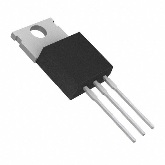
TO−220−3
T SUFFIX
CASE 221AB
4
20 pF
1 2
10 pF 10 k
2.0 k
1.1 k
20 k 20 k
240
0.3
100
750
VI
This device contains 31 active transistors.
Figure 1. Representative Schematic Diagram
9MxxBG
ALYWW
79MxxG
ALYWW
3
DPAK−3
DT SUFFIX
CASE 369C
xx
y
A
WL, L
Y
WW
G
= 05, 08, 12, or 15
= B or C
= Assembly Location
= Wafer Lot
= Year
= Work Week
= Pb−Free Device
ORDERING INFORMATION
See detailed ordering and shipping information in the package
dimensions section on page 6 of this data sheet.
© Semiconductor Components Industries, LLC, 2013
July, 2013 − Rev. 15
1
Publication Order Number:
MC79M00/D
�MC79M00 Series
MAXIMUM RATINGS (TA = 25°C, unless otherwise noted.)
Symbol
Value
Unit
VI
−35
Vdc
TA = 25°C
PD
Internally Limited
W
Thermal Resistance, Junction−to−Ambient
qJA
65
°C/W
Thermal Resistance, Junction−to−Case
qJC
5.0
°C/W
TA = 25°C
PD
Internally Limited
W
Thermal Resistance, Junction−to−Ambient
qJA
92
°C/W
Thermal Resistance, Junction−to−Case
qJC
6.0
°C/W
Storage Junction Temperature
Tstg
−65 to +150
°C
Operating Junction Temperature Range
TJ
−40 to +150
°C
Rating
Input Voltage
Power Dissipation
Case 221A (TO−220−3)
Case 369C (DPAK−3)
Stresses exceeding Maximum Ratings may damage the device. Maximum Ratings are stress ratings only. Functional operation above the
Recommended Operating Conditions is not implied. Extended exposure to stresses above the Recommended Operating Conditions may affect
device reliability.
*This device series contains ESD protection and exceeds the following tests:
Human Body Model 2000 V per MIL_STD_883, Method 3015
Machine Model Method 200 V
MC79M05B, C
ELECTRICAL CHARACTERISTICS (VI = −10 V, IO = 350 mA, Tlow to Thigh (Note 2), unless otherwise noted.)
Characteristic
Output Voltage (TJ = 25°C)
Symbol
Min
Typ
Max
Unit
VO
−4.8
−5.0
−5.2
Vdc
−
−
7.0
2.0
50
30
−
30
100
−4.75
−
−5.25
−
4.3
8.0
−
−
−
−
0.4
0.4
Line Regulation, TJ = 25°C (Note 1)
−7.0 Vdc ≥ VI ≥ −25 Vdc
−8.0 Vdc ≥ VI ≥ −18 Vdc
Regline
Load Regulation, TJ = 25°C (Note 1)
5.0 mA ≤ IO ≤ 500 mA
Regload
Output Voltage
−7.0 Vdc ≥ VI ≥ −25 Vdc, 5.0 mA ≤ IO ≤ 350 mA
VO
Input Bias Current (TJ = 25°C)
IIB
Input Bias Current Change
−8.0 Vdc ≥ VI ≥ −25 Vdc, IO = 350 mA
5.0 mA ≤ IO ≤ 350 mA, VI = −10 V
DIIB
mV
mV
Vdc
mA
mA
Output Noise Voltage, TA = 25°C, 10 Hz ≤ f ≤ 100 kHz
Vn
−
40
−
mV
Ripple Rejection (f = 120 Hz)
RR
54
66
−
dB
−
1.1
−
−
0.2
−
Dropout Voltage
IO = 500 mA, TJ = 25°C
VI−VO
Average Temperature Coefficient of Output Voltage
IO = 5.0 mA, 0°C ≤ TJ ≤ 125°C
DVO/DT
Vdc
mV/°C
1. Load and line regulation are specified at constant temperature. Change in VO due to heating effects must be taken into account separately.
Pulse testing with low duty cycle is used.
2. B = Tlow to Thigh, −40°C < TJ < 125°C C = Tlow to Thigh, 0°C < TJ < 125°C.
http://onsemi.com
2
�MC79M00 Series
MC79M08B, C
ELECTRICAL CHARACTERISTICS (VI = −10 V, IO = 350 mA, Tlow to Thigh (Note 4), unless otherwise noted.)
Characteristic
Output Voltage (TJ = 25°C)
Symbol
Min
Typ
Max
Unit
VO
−7.7
−8.0
−8.3
Vdc
−
−
5.0
3.0
80
50
−
30
100
−7.6
−8.0
−8.4
−
−
8.0
−
−
−
−
0.4
0.4
Line Regulation, TJ = 25°C (Note 3)
−10.5 Vdc ≥ VI ≥ −25 Vdc
−11 Vdc ≥ VI ≥ −21 Vdc
Regline
Load Regulation, TJ = 25°C (Note 3)
5.0 mA ≤ IO ≤ 500 mA
Regload
Output Voltage
−10.5 Vdc ≥ VI ≥ −25 Vdc, 5.0 mA ≤ IO ≤ 350 mA
VO
Input Bias Current (TJ = 25°C)
IIB
Input Bias Current Change
−10.5 Vdc ≥ VI ≥ −25 Vdc, IO = 350 mA
5.0 mA ≤ IO ≤ 350 mA, VI = −10 V
DIIB
mV
mV
Vdc
mA
mA
Output Noise Voltage, TA = 25°C, 10 Hz ≤ f ≤ 100 kHz
Vn
−
60
−
mV
Ripple Rejection (f = 120 Hz)
RR
54
63
−
dB
−
1.1
−
−
0.4
−
Dropout Voltage
IO = 500 mA, TJ = 25°C
VI−VO
Average Temperature Coefficient of Output Voltage
IO = 5.0 mA, 0°C ≤ TJ ≤ 125°C
DVO/DT
Vdc
mV/°C
3. Load and line regulation are specified at constant temperature. Change in VO due to heating effects must be taken into account separately.
Pulse testing with low duty cycle is used.
4. B = Tlow to Thigh, −40°C < TJ < 125°C
C = Tlow to Thigh, 0°C < TJ < 125°C
MC79M12B, C
ELECTRICAL CHARACTERISTICS (VI = −19 V, IO = 350 mA, Tlow to Thigh (Note 6), unless otherwise noted.)
Characteristic
Output Voltage (TJ = 25°C)
Symbol
Min
Typ
Max
Unit
VO
−11.5
−12
−12.5
Vdc
−
−
5.0
3.0
80
50
−
30
240
−11.4
−
−12.6
−
4.4
8.0
−
−
−
−
0.4
0.4
Line Regulation, TJ = 25°C (Note 5)
−14.5 Vdc ≥ VI ≥ −30 Vdc
−15 Vdc ≥ VI ≥ −25 Vdc
Regline
Load Regulation, TJ = 25°C (Note 5)
5.0 mA ≤ IO ≤ 500 mA
Regload
Output Voltage
−14.5 Vdc ≥ VI ≥ −30 Vdc, 5.0 mA ≤ IO ≤ 350 mA
VO
Input Bias Current (TJ = 25°C)
IIB
Input Bias Current Change
−14.5 Vdc ≥ VI ≥ −30 Vdc, IO = 350 mA
5.0 mA ≤ IO ≤ 350 mA, VI = −19 V
DIIB
mV
mV
Vdc
mA
mA
Output Noise Voltage, TA = 25°C, 10 Hz ≤ f ≤ 100 kHz
Vn
−
75
−
mV
Ripple Rejection (f = 120 Hz)
RR
54
60
−
dB
−
1.1
−
−
−0.8
−
Dropout Voltage
IO = 500 mA, TJ = 25°C
VI−VO
Average Temperature Coefficient of Output Voltage
IO = 5.0 mA, 0°C ≤ TJ ≤ 125°C
DVO/DT
Vdc
mV/°C
5. Load and line regulation are specified at constant temperature. Change in VO due to heating effects must be taken into account separately.
Pulse testing with low duty cycle is used.
6. B = Tlow to Thigh, −40°C < TJ < 125°C
C = Tlow to Thigh, 0°C < TJ < 125°C
http://onsemi.com
3
�MC79M00 Series
MC79M15B, C
ELECTRICAL CHARACTERISTICS (VI = − 23 V, IO = 350 mA, Tlow to Thigh (Note 8), unless otherwise noted.)
Characteristic
Output Voltage (TJ = 25°C)
Symbol
Min
Typ
Max
Unit
VO
−14.4
−15
−15.6
Vdc
−
−
5.0
3.0
80
50
−
30
240
−14.25
−
−15.75
−
4.4
8.0
−
−
−
−
0.4
0.4
Line Regulation, TJ = 25°C (Note 7)
−17.5 Vdc ≥ VI ≥ −30 Vdc
−18 Vdc ≥ VI ≥ −28 Vdc
Regline
Load Regulation, TJ = 25°C (Note 7)
5.0 mA ≤ IO ≤ 500 mA
Regload
Output Voltage
−17.5 Vdc ≥ VI ≥ −30 Vdc, 5.0 mA ≤ IO ≤ 350 mA
VO
Input Bias Current (TJ = 25°C)
IIB
Input Bias Current Change
−17.5 Vdc ≥ VI ≥ −30 Vdc, IO = 350 mA
5.0 mA ≤ IO ≤ 350 mA, VI = −23 V
mV
mV
Vdc
mA
mA
DIIB
Output Noise Voltage, TA = 25°C, 10 Hz ≤ f ≤ 100 kHz
Vn
−
90
−
mV
Ripple Rejection (f = 120 Hz)
RR
54
60
−
dB
−
1.1
−
−
−1.0
−
Dropout Voltage
IO = 500 mA, TJ = 25°C
VI−VO
Average Temperature Coefficient of Output Voltage
IO = 5.0 mA, 0°C ≤ TJ ≤ 125°C
Vdc
mV/°C
DVO/DT
JUNCTION‐TO‐AIR (°C/W)
R θ JA, THERMAL RESISTANCE
100
90
2.0
ÎÎÎÎ
ÎÎÎÎ
ÎÎÎÎ
ÎÎÎÎ
80
Minimum
Size Pad
70
2.4
PD(max) for TA = 50°C
Free Air
Mounted
Vertically
60
2.0 oz. Copper
L
1.6
L
1.2
0.8
50
0.4
RqJA
40
0
0
5.0
10
15
20
25
30
L, LENGTH OF COPPER (mm)
Figure 1. DPAK−3 Thermal Resistance and Maximum
Power Dissipation versus P.C.B. Copper Length
http://onsemi.com
4
PD, MAXIMUM POWER DISSIPATION (W)
7. Load and line regulation are specified at constant temperature. Change in VO due to heating effects must be taken into account separately.
Pulse testing with low duty cycle is used.
8. B = Tlow to Thigh, −40°C < TJ < 125°C
C = Tlow to Thigh, 0°C < TJ < 125°C
�MC79M00 Series
Protection Diodes
Diode D2 prevents output capacitor from discharging thru
the MC79M15 during an input short circuit or fast switch off
of power supply.
When external capacitors are used with MC79M00 series
regulator it is sometimes necessary to add protection diodes
to prevent the capacitors from discharging through low
current points into the regulator or from output polarity
reversals. Generally, no protection diode is required for
values of output capacitance less then 10mF. Figure 2 shows
the MC79M15 with the recommended protection diodes.
• Opposite Polarity Protection
Diode D1 protects the regulator from output polarity
reversals during startup, power off and short-circuit
operation.
• Reverse-bias Protection
Gnd
+
1.0 mF
1.0 mF
Gnd
+
D1
MBRS140
or Equiv
MC79M15
-�20 V
Input
-15 V
Output
D2
MBRS140
or Equiv
Figure 2. Protection Diodes
http://onsemi.com
5
�MC79M00 Series
ORDERING INFORMATION
Device
Output Voltage
Tolerance
Operating
Temperature Range
MC79M05BDT
MC79M05BDTG
MC79M05BDTRK
TJ = −40°C to +125°C
MC79M05BDTRKG
MC79M05BT
MC79M05BTG
MC79M05CDT
MC79M05CDTG
MC79M05CDTRK
TJ = 0°C to +125°C
MC79M05CDTRKG
MC79M05CT
MC79M05CTG
MC79M08BDT
MC79M08BDTRK
MC79M08BDTRKG
TJ = −40°C to +125°C
MC79M08BT
MC79M08BTG
MC79M08CDT
4.0%
MC79M08CDTG
MC79M08CDTRK
MC79M08CDTRKG
TJ = 0°C to +125°C
MC79M08CT
MC79M08CTG
MC79M12BDT
MC79M12BDTG
MC79M12BDTRK
MC79M12BDTRKG
TJ = −40°C to +125°C
MC79M12BT
MC79M12BTG
MC79M12CDT
MC79M12CDTG
MC79M12CDTRK
MC79M12CDTRKG
TJ = 0°C to +125°C
MC79M12CT
MC79M12CTG
Package
Shipping†
DPAK
DPAK
(Pb−Free)
75 Units / Rail
DPAK
DPAK
(Pb−Free)
2500 Units / Reel
TO−220
TO−220
(Pb−Free)
50 Units / Rail
DPAK
DPAK
(Pb−Free)
75 Units / Rail
DPAK
DPAK
(Pb−Free)
2500 Units / Reel
TO−220
TO−220
(Pb−Free)
50 Units / Rail
DPAK
DPAK
DPAK
(Pb−Free)
75 Units / Rail
2500 Units / Reel
TO−220
TO−220
(Pb−Free)
50 Units / Rail
DPAK
DPAK
(Pb−Free)
75 Units / Rail
DPAK
DPAK
(Pb−Free)
2500 Units / Reel
TO−220
TO−220
(Pb−Free)
50 Units / Rail
DPAK
DPAK
(Pb−Free)
75 Units / Rail
DPAK
DPAK
(Pb−Free)
2500 Units / Reel
TO−220
TO−220
(Pb−Free)
50 Units / Rail
DPAK
DPAK
(Pb−Free)
75 Units / Rail
DPAK
DPAK
(Pb−Free)
2500 Units / Reel
TO−220
TO−220
(Pb−Free)
50 Units / Rail
75 Units / Rail
2500 Units / Reel
50 Units / Rail
75 Units / Rail
2500 Units / Reel
50 Units / Rail
2500 Units / Reel
50 Units / Rail
75 Units / Rail
2500 Units / Reel
50 Units / Rail
75 Units / Rail
2500 Units / Reel
50 Units / Rail
75 Units / Rail
2500 Units / Reel
50 Units / Rail
†For information on tape and reel specifications, including part orientation and tape sizes, please refer to our Tape and Reel Packaging
Specifications Brochure, BRD8011/D.
http://onsemi.com
6
�MC79M00 Series
ORDERING INFORMATION
Device
Output Voltage
Tolerance
Operating
Temperature Range
MC79M15BDT
MC79M15BDTG
MC79M15BDTRK
TJ = −40°C to +125°C
MC79M15BDTRKG
MC79M15BT
MC79M15BTG
MC79M15CDT
4.0%
MC79M15CDTG
MC79M15CDTRK
MC79M15CDTRKG
TJ = 0°C to +125°C
MC79M15CT
MC79M15CTG
Package
Shipping[
DPAK
75 Units / Rail
DPAK
(Pb−Free)
75 Units / Rail
DPAK
2500 Units / Reel
DPAK
(Pb−Free)
2500 Units / Reel
TO−220
50 Units / Rail
TO−220
(Pb−Free)
50 Units / Rail
DPAK
75 Units / Rail
DPAK
(Pb−Free)
75 Units / Rail
DPAK
2500 Units / Reel
DPAK
(Pb−Free)
2500 Units / Reel
TO−220
50 Units / Rail
TO−220
(Pb−Free)
50 Units / Rail
†For information on tape and reel specifications, including part orientation and tape sizes, please refer to our Tape and Reel Packaging
Specifications Brochure, BRD8011/D.
http://onsemi.com
7
�MECHANICAL CASE OUTLINE
PACKAGE DIMENSIONS
TO−220, SINGLE GAUGE
CASE 221AB−01
ISSUE A
−T−
B
F
T
SCALE 1:1
SEATING
PLANE
C
S
DATE 16 NOV 2010
NOTES:
1. DIMENSIONING AND TOLERANCING PER ANSI Y14.5M, 1982.
2. CONTROLLING DIMENSION: INCHES.
3. DIMENSION Z DEFINES A ZONE WHERE ALL BODY AND
LEAD IRREGULARITIES ARE ALLOWED.
4. PRODUCT SHIPPED PRIOR TO 2008 HAD DIMENSIONS
S = 0.045 - 0.055 INCHES (1.143 - 1.397 MM)
4
DIM
A
B
C
D
F
G
H
J
K
L
N
Q
R
S
T
U
V
Z
A
Q
U
1 2 3
H
K
Z
L
R
V
J
G
D
N
INCHES
MIN
MAX
0.570
0.620
0.380
0.405
0.160
0.190
0.025
0.035
0.142
0.147
0.095
0.105
0.110
0.155
0.018
0.025
0.500
0.562
0.045
0.060
0.190
0.210
0.100
0.120
0.080
0.110
0.020
0.024
0.235
0.255
0.000
0.050
0.045
----0.080
MILLIMETERS
MIN
MAX
14.48
15.75
9.66
10.28
4.07
4.82
0.64
0.88
3.61
3.73
2.42
2.66
2.80
3.93
0.46
0.64
12.70
14.27
1.15
1.52
4.83
5.33
2.54
3.04
2.04
2.79
0.508
0.61
5.97
6.47
0.00
1.27
1.15
----2.04
STYLE 1:
PIN 1.
2.
3.
4.
BASE
COLLECTOR
EMITTER
COLLECTOR
STYLE 2:
PIN 1.
2.
3.
4.
BASE
EMITTER
COLLECTOR
EMITTER
STYLE 3:
PIN 1.
2.
3.
4.
CATHODE
ANODE
GATE
ANODE
STYLE 4:
PIN 1.
2.
3.
4.
MAIN TERMINAL 1
MAIN TERMINAL 2
GATE
MAIN TERMINAL 2
STYLE 5:
PIN 1.
2.
3.
4.
GATE
DRAIN
SOURCE
DRAIN
STYLE 6:
PIN 1.
2.
3.
4.
ANODE
CATHODE
ANODE
CATHODE
STYLE 7:
PIN 1.
2.
3.
4.
CATHODE
ANODE
CATHODE
ANODE
STYLE 8:
PIN 1.
2.
3.
4.
CATHODE
ANODE
EXTERNAL TRIP/DELAY
ANODE
STYLE 9:
PIN 1.
2.
3.
4.
GATE
COLLECTOR
EMITTER
COLLECTOR
STYLE 10:
PIN 1.
2.
3.
4.
GATE
SOURCE
DRAIN
SOURCE
STYLE 11:
PIN 1.
2.
3.
4.
DRAIN
SOURCE
GATE
SOURCE
DOCUMENT NUMBER:
DESCRIPTION:
98AON23085D
TO−220, SINGLE GAUGE
Electronic versions are uncontrolled except when accessed directly from the Document Repository.
Printed versions are uncontrolled except when stamped “CONTROLLED COPY” in red.
PAGE 1 OF 1
ON Semiconductor and
are trademarks of Semiconductor Components Industries, LLC dba ON Semiconductor or its subsidiaries in the United States and/or other countries.
ON Semiconductor reserves the right to make changes without further notice to any products herein. ON Semiconductor makes no warranty, representation or guarantee regarding
the suitability of its products for any particular purpose, nor does ON Semiconductor assume any liability arising out of the application or use of any product or circuit, and specifically
disclaims any and all liability, including without limitation special, consequential or incidental damages. ON Semiconductor does not convey any license under its patent rights nor the
rights of others.
© Semiconductor Components Industries, LLC, 2019
www.onsemi.com
�MECHANICAL CASE OUTLINE
PACKAGE DIMENSIONS
DPAK (SINGLE GAUGE)
CASE 369C
ISSUE F
4
1 2
DATE 21 JUL 2015
3
SCALE 1:1
A
E
b3
C
A
B
c2
4
L3
Z
D
1
L4
2
3
NOTE 7
b2
e
c
SIDE VIEW
b
0.005 (0.13)
TOP VIEW
H
DETAIL A
M
BOTTOM VIEW
C
Z
H
L2
GAUGE
PLANE
C
L
L1
DETAIL A
Z
SEATING
PLANE
BOTTOM VIEW
A1
ALTERNATE
CONSTRUCTIONS
ROTATED 905 CW
STYLE 1:
PIN 1. BASE
2. COLLECTOR
3. EMITTER
4. COLLECTOR
STYLE 6:
PIN 1. MT1
2. MT2
3. GATE
4. MT2
STYLE 2:
PIN 1. GATE
2. DRAIN
3. SOURCE
4. DRAIN
STYLE 7:
PIN 1. GATE
2. COLLECTOR
3. EMITTER
4. COLLECTOR
STYLE 3:
PIN 1. ANODE
2. CATHODE
3. ANODE
4. CATHODE
STYLE 8:
PIN 1. N/C
2. CATHODE
3. ANODE
4. CATHODE
STYLE 4:
PIN 1. CATHODE
2. ANODE
3. GATE
4. ANODE
STYLE 9:
STYLE 10:
PIN 1. ANODE
PIN 1. CATHODE
2. CATHODE
2. ANODE
3. RESISTOR ADJUST
3. CATHODE
4. CATHODE
4. ANODE
SOLDERING FOOTPRINT*
6.20
0.244
2.58
0.102
5.80
0.228
INCHES
MIN
MAX
0.086 0.094
0.000 0.005
0.025 0.035
0.028 0.045
0.180 0.215
0.018 0.024
0.018 0.024
0.235 0.245
0.250 0.265
0.090 BSC
0.370 0.410
0.055 0.070
0.114 REF
0.020 BSC
0.035 0.050
−−− 0.040
0.155
−−−
MILLIMETERS
MIN
MAX
2.18
2.38
0.00
0.13
0.63
0.89
0.72
1.14
4.57
5.46
0.46
0.61
0.46
0.61
5.97
6.22
6.35
6.73
2.29 BSC
9.40 10.41
1.40
1.78
2.90 REF
0.51 BSC
0.89
1.27
−−−
1.01
3.93
−−−
GENERIC
MARKING DIAGRAM*
XXXXXXG
ALYWW
AYWW
XXX
XXXXXG
IC
Discrete
= Device Code
= Assembly Location
= Wafer Lot
= Year
= Work Week
= Pb−Free Package
*This information is generic. Please refer to
device data sheet for actual part marking.
Pb−Free indicator, “G” or microdot “G”, may
or may not be present. Some products may
not follow the Generic Marking.
6.17
0.243
SCALE 3:1
DIM
A
A1
b
b2
b3
c
c2
D
E
e
H
L
L1
L2
L3
L4
Z
XXXXXX
A
L
Y
WW
G
3.00
0.118
1.60
0.063
STYLE 5:
PIN 1. GATE
2. ANODE
3. CATHODE
4. ANODE
NOTES:
1. DIMENSIONING AND TOLERANCING PER ASME
Y14.5M, 1994.
2. CONTROLLING DIMENSION: INCHES.
3. THERMAL PAD CONTOUR OPTIONAL WITHIN DIMENSIONS b3, L3 and Z.
4. DIMENSIONS D AND E DO NOT INCLUDE MOLD
FLASH, PROTRUSIONS, OR BURRS. MOLD
FLASH, PROTRUSIONS, OR GATE BURRS SHALL
NOT EXCEED 0.006 INCHES PER SIDE.
5. DIMENSIONS D AND E ARE DETERMINED AT THE
OUTERMOST EXTREMES OF THE PLASTIC BODY.
6. DATUMS A AND B ARE DETERMINED AT DATUM
PLANE H.
7. OPTIONAL MOLD FEATURE.
mm Ǔ
ǒinches
*For additional information on our Pb−Free strategy and soldering
details, please download the ON Semiconductor Soldering and
Mounting Techniques Reference Manual, SOLDERRM/D.
DOCUMENT NUMBER:
DESCRIPTION:
98AON10527D
DPAK (SINGLE GAUGE)
Electronic versions are uncontrolled except when accessed directly from the Document Repository.
Printed versions are uncontrolled except when stamped “CONTROLLED COPY” in red.
PAGE 1 OF 1
onsemi and
are trademarks of Semiconductor Components Industries, LLC dba onsemi or its subsidiaries in the United States and/or other countries. onsemi reserves
the right to make changes without further notice to any products herein. onsemi makes no warranty, representation or guarantee regarding the suitability of its products for any particular
purpose, nor does onsemi assume any liability arising out of the application or use of any product or circuit, and specifically disclaims any and all liability, including without limitation
special, consequential or incidental damages. onsemi does not convey any license under its patent rights nor the rights of others.
© Semiconductor Components Industries, LLC, 2018
www.onsemi.com
�onsemi,
, and other names, marks, and brands are registered and/or common law trademarks of Semiconductor Components Industries, LLC dba “onsemi” or its affiliates
and/or subsidiaries in the United States and/or other countries. onsemi owns the rights to a number of patents, trademarks, copyrights, trade secrets, and other intellectual property.
A listing of onsemi’s product/patent coverage may be accessed at www.onsemi.com/site/pdf/Patent−Marking.pdf. onsemi reserves the right to make changes at any time to any
products or information herein, without notice. The information herein is provided “as−is” and onsemi makes no warranty, representation or guarantee regarding the accuracy of the
information, product features, availability, functionality, or suitability of its products for any particular purpose, nor does onsemi assume any liability arising out of the application or use
of any product or circuit, and specifically disclaims any and all liability, including without limitation special, consequential or incidental damages. Buyer is responsible for its products
and applications using onsemi products, including compliance with all laws, regulations and safety requirements or standards, regardless of any support or applications information
provided by onsemi. “Typical” parameters which may be provided in onsemi data sheets and/or specifications can and do vary in different applications and actual performance may
vary over time. All operating parameters, including “Typicals” must be validated for each customer application by customer’s technical experts. onsemi does not convey any license
under any of its intellectual property rights nor the rights of others. onsemi products are not designed, intended, or authorized for use as a critical component in life support systems
or any FDA Class 3 medical devices or medical devices with a same or similar classification in a foreign jurisdiction or any devices intended for implantation in the human body. Should
Buyer purchase or use onsemi products for any such unintended or unauthorized application, Buyer shall indemnify and hold onsemi and its officers, employees, subsidiaries, affiliates,
and distributors harmless against all claims, costs, damages, and expenses, and reasonable attorney fees arising out of, directly or indirectly, any claim of personal injury or death
associated with such unintended or unauthorized use, even if such claim alleges that onsemi was negligent regarding the design or manufacture of the part. onsemi is an Equal
Opportunity/Affirmative Action Employer. This literature is subject to all applicable copyright laws and is not for resale in any manner.
PUBLICATION ORDERING INFORMATION
LITERATURE FULFILLMENT:
Email Requests to: orderlit@onsemi.com
onsemi Website: www.onsemi.com
◊
TECHNICAL SUPPORT
North American Technical Support:
Voice Mail: 1 800−282−9855 Toll Free USA/Canada
Phone: 011 421 33 790 2910
Europe, Middle East and Africa Technical Support:
Phone: 00421 33 790 2910
For additional information, please contact your local Sales Representative
�