Is Now Part of
To learn more about ON Semiconductor, please visit our website at
www.onsemi.com
Please note: As part of the Fairchild Semiconductor integration, some of the Fairchild orderable part numbers
will need to change in order to meet ON Semiconductor’s system requirements. Since the ON Semiconductor
product management systems do not have the ability to manage part nomenclature that utilizes an underscore
(_), the underscore (_) in the Fairchild part numbers will be changed to a dash (-). This document may contain
device numbers with an underscore (_). Please check the ON Semiconductor website to verify the updated
device numbers. The most current and up-to-date ordering information can be found at www.onsemi.com. Please
email any questions regarding the system integration to Fairchild_questions@onsemi.com.
ON Semiconductor and the ON Semiconductor logo are trademarks of Semiconductor Components Industries, LLC dba ON Semiconductor or its subsidiaries in the United States and/or other countries. ON Semiconductor owns the rights to a number
of patents, trademarks, copyrights, trade secrets, and other intellectual property. A listing of ON Semiconductor’s product/patent coverage may be accessed at www.onsemi.com/site/pdf/Patent-Marking.pdf. ON Semiconductor reserves the right
to make changes without further notice to any products herein. ON Semiconductor makes no warranty, representation or guarantee regarding the suitability of its products for any particular purpose, nor does ON Semiconductor assume any liability
arising out of the application or use of any product or circuit, and specifically disclaims any and all liability, including without limitation special, consequential or incidental damages. Buyer is responsible for its products and applications using ON
Semiconductor products, including compliance with all laws, regulations and safety requirements or standards, regardless of any support or applications information provided by ON Semiconductor. “Typical” parameters which may be provided in ON
Semiconductor data sheets and/or specifications can and do vary in different applications and actual performance may vary over time. All operating parameters, including “Typicals” must be validated for each customer application by customer’s
technical experts. ON Semiconductor does not convey any license under its patent rights nor the rights of others. ON Semiconductor products are not designed, intended, or authorized for use as a critical component in life support systems or any FDA
Class 3 medical devices or medical devices with a same or similar classification in a foreign jurisdiction or any devices intended for implantation in the human body. Should Buyer purchase or use ON Semiconductor products for any such unintended
or unauthorized application, Buyer shall indemnify and hold ON Semiconductor and its officers, employees, subsidiaries, affiliates, and distributors harmless against all claims, costs, damages, and expenses, and reasonable attorney fees arising out
of, directly or indirectly, any claim of personal injury or death associated with such unintended or unauthorized use, even if such claim alleges that ON Semiconductor was negligent regarding the design or manufacture of the part. ON Semiconductor
is an Equal Opportunity/Affirmative Action Employer. This literature is subject to all applicable copyright laws and is not for resale in any manner.
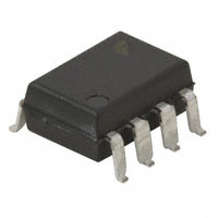
�MCT6, MCT61, MCT62
8-Pin Dual Channel Phototransistor Optocouplers
Features
Description
• Two Isolated Channels Per Package
• Safety and Regulatory Approvals:
– UL1577, 5,000 VACRMS for 1 Minute
– DIN-EN/IEC60747-5-5, 890 V Peak Working
Insulation Voltage
The general purpose optocouplers, MCT6, MCT61, and
MCT62, have two isolated channels in a standard plastic
8-pin dual-in-line (DIP) package for density applications.
Each channel consists of a gallium arsenide infrared
emitting diode driving a NPN silicon planar
phototransistor. For four channel applications, two
packages fit into a standard 16-pin DIP socket.
Applications
•
•
•
•
•
•
•
•
•
•
•
•
•
AC line/digital logic – isolate high voltage transients
Digital logic/digital logic – eliminate spurious grounds
Digital logic/AC triac control – isolate high voltage
transients
Twisted pair line receiver – eliminate ground loop
feedthrough
Telephone/telegraph line receiver – isolate high
voltage transients
High frequency power supply feedback control –
maintain floating grounds and transients
Relay contact monitor – isolate floating grounds and
transients
Power supply monitor – isolate transients
Functional Schematic
ANODE 1
Package Outlines
8 EMITTER
8
1
CATHODE 2
7 COLLECTOR
CATHODE 3
6 COLLECTOR
8
8
1
ANODE 4
5 EMITTER
1
Figure 2. Package Outlines
Figure 1. Schematic
©2006 Fairchild Semiconductor Corporation
MCT6, MCT61, MCT62 Rev.1.6
www.fairchildsemi.com
MCT6, MCT61, MCT62 8-Pin Dual Channel Phototransistor Optocouplers
August 2016
�As per DIN EN/IEC 60747-5-5, this optocoupler is suitable for “safe electrical insulation” only within the safety limit
data. Compliance with the safety ratings shall be ensured by means of protective circuits.
Parameter
Installation Classifications per DIN VDE
0110/1.89 Table 1, For Rated Mains Voltage
Characteristics
< 150 VRMS
I–IV
< 300 VRMS
I–IV
Climatic Classification
55/115/21
Pollution Degree (DIN VDE 0110/1.89)
2
Comparative Tracking Index
Symbol
175
Value
Unit
Input-to-Output Test Voltage, Method A, VIORM x 1.6 = VPR,
Type and Sample Test with tm = 10 s, Partial Discharge < 5 pC
1424
Vpeak
Input-to-Output Test Voltage, Method B, VIORM x 1.875 = VPR,
100% Production Test with tm = 1 s, Partial Discharge < 5 pC
1668
Vpeak
VIORM
Maximum Working Insulation Voltage
890
Vpeak
VIOTM
Highest Allowable Over-Voltage
8000
Vpeak
7
mm
VPR
Parameter
External Creepage
7
mm
0.4
mm
Case
Temperature(1)
175
°C
Input
Current(1)
60
mA
150
mW
> 109
External Clearance
DTI
TS
IS,INPUT
Distance Through Insulation (Insulation Thickness)
PS,OUTPUT Output
RIO
Power(1)
Insulation Resistance at TS, VIO = 500 V(1)
Note:
1. Safety limit values – maximum values allowed in the event of a failure.
©2006 Fairchild Semiconductor Corporation
MCT6, MCT61, MCT62 Rev.1.6
www.fairchildsemi.com
2
MCT6, MCT61, MCT62 8-Pin Dual Channel Phototransistor Optocouplers
Safety and Insulation Ratings
�Stresses exceeding the absolute maximum ratings may damage the device. The device may not function or be operable above the recommended operating conditions and stressing the parts to these levels is not recommended. In addition, extended exposure to stresses above the recommended operating conditions may affect device reliability. The
absolute maximum ratings are stress ratings only. TA = 25°C unless otherwise specified.
Symbol
Parameter
Value
Unit
TSTG
Storage Temperature
-55 to +150
°C
TOPR
Operating Temperature
-55 to +100
°C
Junction Temperature
-55 to +125
°C
260 for 10 seconds
°C
Total Device Power Dissipation @ TA = 25°C
400
mW
Derate Above 25°C
5.33
mW/°C
DC / Average Forward Input Current
60
mA
Forward Current - Peak (PW = 1μs, 300pps)
3
A
Reverse Input Voltage
3
V
Total Power Dissipation @ TA = 25°C
100
mW
Derate Above 25°C
1.3
mW/°C
Continuous Collector Current
30
mA
Total Power Dissipation @ TA = 25°C
150
mW
Derate Above 25°C
2.0
mW/°C
TJ
TSOL
PD
Lead Solder Temperature
EMITTER (Each channel)
IF
IF(pk)
VR
PD(EMITTER)
DETECTOR
IC
PD(DETECTOR)
©2006 Fairchild Semiconductor Corporation
MCT6, MCT61, MCT62 Rev.1.6
www.fairchildsemi.com
3
MCT6, MCT61, MCT62 8-Pin Dual Channel Phototransistor Optocouplers
Absolute Maximum Ratings
�TA = 25°C unless otherwise specified.
Individual Component Characteristics
Symbol
Parameter
Test Conditions
Min.
Typ.
Max.
Unit
1.2
1.5
V
EMITTER
VF
Input Forward Voltage
IF = 20 mA
VR
Reverse Voltage
IR = 10 μA
IR
Reverse Leakage Current
VR = 5 V
CJ
Junction Capacitance
VF = 0 V, f = 1 MHz
3
25
0.001
V
10
μA
50
pF
DETECTOR
BVCEO
Collector-to-Emitter Breakdown
Voltage
IC = 1.0 mA, IF = 0
30
85
V
BVECO
Emitter-to-Collector Breakdown
Voltage
IE = 100 μA, IF = 0
6
13
V
ICEO
Collector-to-Emitter Dark Current VCE = 10 V, IF = 0
5
CCE
Capacitance
8
VCE = 0 V, f = 1 MHz
100
nA
pF
Transfer Characteristics
Symbol
Parameter
Device
Test Conditions
Min.
Typ.
Max.
Unit
DC CHARACTERISTICS
CTR
VCE(SAT)
IF = 10 mA, VCE = 10 V
MCT6
Current Transfer Ratio, CollectorMCT61
to-Emitter
MCT62
Saturation Voltage, Collector-toEmitter
IF = 5 mA, VCE = 5 V
ALL
20
50
%
100
IF = 16 mA, IC = 2 mA
0.15
0.4
V
Typ.
Max.
Unit
AC CHARACTERISTICS
Symbol
Parameter
Test Conditions
Min.
Non-Saturated
TON
Turn-On Time
TOFF
Turn-Off Time
TR
Rise Time
TF
Fall Time
RL = 100 Ω, IC = 2 mA, VCC = 10 V
3.0
µs
3.0
µs
2.4
µs
2.4
µs
2.4
µs
25.0
µs
Saturated
TON
Turn-On Time
TOFF
Turn-Off Time
IF = 16 mA, RL = 1.9 kΩ, VCE = 5 V
Isolation Characteristics
Symbol
Parameter
Test Conditions
Min.
VISO
Input-Output Isolation Voltage
II-O ≤ 10 µA, t = 1 Minute
5,000
CISO
Isolation Capacitance
f = 1 MHz
RISO
Isolation Resistance
©2006 Fairchild Semiconductor Corporation
MCT6, MCT61, MCT62 Rev.1.6
Typ.
VI-O = 500 VDC
Unit
VACRMS
0.5
1011
Max.
pF
Ω
www.fairchildsemi.com
4
MCT6, MCT61, MCT62 8-Pin Dual Channel Phototransistor Optocouplers
Electrical Characteristics
�1.6
1.4
VCE = 5.0�V
TA = 25°C
1.4
1.0
NORMALIZED CTR
NORMALIZED CTR
1.2
Normalized to
IF = 10�mA
0.8
0.6
0.4
1.0
IF = 10�mA
0.8
0.6
0.2
0.0
0
5
10
15
IF - FORWARD CURRENT (mA)
IF = 20�mA
-50
-25
0
25
50
75
100
TA - AMBIENT TEMPERATURE (°C)
125
)LJ����1RUPDOL]HG�&75�YV��$PELHQW�7HPSHUDWXUH
1000
101
IF = 10�mA
VCC =10�V
TA = 25°C
VCE = 10�V
0
SWITCHING SPEED (μs)
10
Normalized to
IF = 10�mA
TA = 25°C
0.4
-75
20
)LJ����1RUPDOL]HG�&75�YV��)RUZDUG�&XUUHQW
ICEO - COLLECTOR-EMITTER DARK CURRENT (μA)
IF = 5�mA
1.2
10 -1
10 -2
10 -3
10 -4
100
T2))
T)
10
T21
1
T5
10 -5
10 -6
0
25
50
75
100
125
0.1
1�
10�
R - LOAD RESISTOR (kΩ)
0.1�
TA - AMBIENT TEMPERATURE (°C)
100�
)LJ����6ZLWFKLQJ�6SHHG�YV��/RDG�5HVLVWRU
)LJ����'DUN�&XUUHQW�YV��$PELHQW�7HPSHUDWXUH
1.8
100
TA = 25°C
VCE (SAT) - COLLECTOR-EMITTER
SATURATION VOLTAGE (V)
VF - FORWARD VOLTATGE (V)
1.7
1.6
1.5
1.4
TA = 55°C
1.3
TA = 25°C
1.2
10
1
IF = 2.5�mA
0.1
IF =20�mA
0.01
IF =10�mA
1.1
IF = 5mA
TA = 100°C
1.0
1
0.001
0.01
10
100
IF - LED FORWARD CURRENT (mA)
)LJ����/('�)RUZDUG�9ROWDJH�YV��)RUZDUG�&XUUHQW
©2006 Fairchild Semiconductor Corporation
MCT6, MCT61, MCT62 Rev.1.6
0.1
1
IC - COLLECTOR CURRENT (mA)
10
)LJ����&ROOHFWRU�(PLWWHU�6DWXUDWLRQ�9ROWDJH�
YV��&ROOHFWRU�&XUUHQW
www.fairchildsemi.com
5
MCT6, MCT61, MCT62 8-Pin Dual Channel Phototransistor Optocouplers
Typical Performance Curves
�TEST CIRCUIT
WAVE FORMS
VCC = 10 V
INPUT PULSE
IC
IF
INPUT
RL
10%
OUTPUT
OUTPUT PULSE
90%
RBE
75
721
7)
72))
Adjust IF to produce IC = 2 mA
Figure 9. Switching Time Test Circuit and Waveforms
©2006 Fairchild Semiconductor Corporation
MCT6, MCT61, MCT62 Rev.1.6
www.fairchildsemi.com
6
MCT6, MCT61, MCT62 8-Pin Dual Channel Phototransistor Optocouplers
Switching Time Test Circuit and Waveforms
�MCT6, MCT61, MCT62 8-Pin Dual Channel Phototransistor Optocouplers
Reflow Profile
Temperature (°C)
Max. Ramp-up Rate = 3°C/S
TP
Max. Ramp-down Rate = 6°C/S
260
240
TL
220
Tsmax
200
180
Preheat Area
160
Tsmin
140
120
100
80
60
40
20
0
120
tP
tL
ts
240
360
Time 25°C to Peak
Time (seconds)
Profile Feature
Pb-Free Assembly Profile
Temperature Min. (Tsmin)
150°C
Temperature Max. (Tsmax)
200°C
Time (tS) from (Tsmin to Tsmax)
60–120 seconds
Ramp-up Rate (tL to tP)
3°C/second max.
Liquidous Temperature (TL)
217°C
Time (tL) Maintained Above (TL)
60–150 seconds
Peak Body Package Temperature
260°C +0°C / –5°C
Time (tP) within 5°C of 260°C
30 seconds
Ramp-down Rate (TP to TL)
6°C/second max.
Time 25°C to Peak Temperature
©2006 Fairchild Semiconductor Corporation
MCT6, MCT61, MCT62 Rev.1.6
8 minutes max.
www.fairchildsemi.com
7
�Part Number
Package
Packing Method
MCT6
DIP 8-Pin
Tube (50 units per tube)
MCT6S
SMT 8-Pin (Lead Bend)
Tube (50 units per tube)
MCT6SD
SMT 8-Pin
Tape and Reel (1,000 units per reel)
MCT6300
DIN EN/IEC 60747-5-5 Option
Tube (50 units per tube)
MCT63S
SMT 8-Pin (Lead Bend); DIN EN/IEC 60747-5-5 Option
Tube (50 units per tube)
MCT63SD
SMT 8-Pin; DIN EN/IEC 60747-5-5 Option
Tape and Reel (1,000 units per reel)
MCT6300W
0.4” Lead Spacing; DIN EN/IEC 60747-5-5 Option
Tube (50 units per tube)
Note
1. The product orderable part number system listed in this table also applies to the MCT61 and MCT62.
Marking Information
1
MCT6
V
3
XX YY
H
2
6
5
4
Figure 10. Top Mark
Table 1. Top Mark Definitions
1
Fairchild Logo
2
Device Number
3
DIN EN/IEC60747-5-5 Option (only appears on component ordered with this option)
4
Two-Digit Year Code, e.g., “16”
5
Digit Work Week, Ranging from “01” to “53”
6
Assembly Package Code
©2006 Fairchild Semiconductor Corporation
MCT6, MCT61, MCT62 Rev.1.6
www.fairchildsemi.com
8
MCT6, MCT61, MCT62 8-Pin Dual Channel Phototransistor Optocouplers
Ordering Information
����ON Semiconductor and
are trademarks of Semiconductor Components Industries, LLC dba ON Semiconductor or its subsidiaries in the United States and/or other countries.
ON Semiconductor owns the rights to a number of patents, trademarks, copyrights, trade secrets, and other intellectual property. A listing of ON Semiconductor’s product/patent
coverage may be accessed at www.onsemi.com/site/pdf/Patent−Marking.pdf. ON Semiconductor reserves the right to make changes without further notice to any products herein.
ON Semiconductor makes no warranty, representation or guarantee regarding the suitability of its products for any particular purpose, nor does ON Semiconductor assume any liability
arising out of the application or use of any product or circuit, and specifically disclaims any and all liability, including without limitation special, consequential or incidental damages.
Buyer is responsible for its products and applications using ON Semiconductor products, including compliance with all laws, regulations and safety requirements or standards,
regardless of any support or applications information provided by ON Semiconductor. “Typical” parameters which may be provided in ON Semiconductor data sheets and/or
specifications can and do vary in different applications and actual performance may vary over time. All operating parameters, including “Typicals” must be validated for each customer
application by customer’s technical experts. ON Semiconductor does not convey any license under its patent rights nor the rights of others. ON Semiconductor products are not
designed, intended, or authorized for use as a critical component in life support systems or any FDA Class 3 medical devices or medical devices with a same or similar classification
in a foreign jurisdiction or any devices intended for implantation in the human body. Should Buyer purchase or use ON Semiconductor products for any such unintended or unauthorized
application, Buyer shall indemnify and hold ON Semiconductor and its officers, employees, subsidiaries, affiliates, and distributors harmless against all claims, costs, damages, and
expenses, and reasonable attorney fees arising out of, directly or indirectly, any claim of personal injury or death associated with such unintended or unauthorized use, even if such
claim alleges that ON Semiconductor was negligent regarding the design or manufacture of the part. ON Semiconductor is an Equal Opportunity/Affirmative Action Employer. This
literature is subject to all applicable copyright laws and is not for resale in any manner.
PUBLICATION ORDERING INFORMATION
LITERATURE FULFILLMENT:
Literature Distribution Center for ON Semiconductor
19521 E. 32nd Pkwy, Aurora, Colorado 80011 USA
Phone: 303−675−2175 or 800−344−3860 Toll Free USA/Canada
Fax: 303−675−2176 or 800−344−3867 Toll Free USA/Canada
Email: orderlit@onsemi.com
© Semiconductor Components Industries, LLC
N. American Technical Support: 800−282−9855 Toll Free
USA/Canada
Europe, Middle East and Africa Technical Support:
Phone: 421 33 790 2910
Japan Customer Focus Center
Phone: 81−3−5817−1050
www.onsemi.com
1
ON Semiconductor Website: www.onsemi.com
Order Literature: http://www.onsemi.com/orderlit
For additional information, please contact your local
Sales Representative
www.onsemi.com
�