DATA SHEET
www.onsemi.com
Bridge Rectifiers,
Single-Phase, MicroDIP, 1 A
MDB8S Series
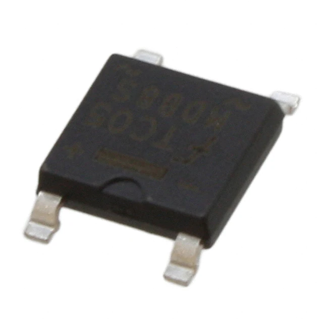
TSSOP4
CASE 948BS
MDB6S, MDB8S, MDB10S
~
Description
With the ever pressing need to improve power supply efficiency
and reliability, the MDBxS family is focused on offering a best in class
small form factor combined with best inclass efficient rectifier
performance.
The “S” family offers industry leading balance of efficiency, size,
and cost. They offer designers improved efficiency by achieving an
industry leading VF of 0.935 V Typ. at 1 A 25°C, and a VF of 1.165 V
Typ. at 5 A 25°C. These lower VF values offer roughly a 5% efficiency
improvement over measured competitive same form factor devices.
This lower VF vs. competitive devices results in cooler and more
efficient power supply operation.
The design supports a 30 A IFSM rating to absorb high surge currents
and offers rated breakdown voltages up to 1000 V.
Finally, the MDBxS family achieves all this in a small form factor
micro−dip package − offering a max height of 1.6 mm, and requiring
only 35 mm2 of board space.
+
IN
~
−
MARKING DIAGRAM
−
+
$Y&Z&3
MDBXS
Features
•
•
•
•
•
•
•
•
•
•
Low Package Profile: 1.60 mm (max)
Small Area Requirements: 35 mm2
Efficient VF
0.935 V (Typ) at 1 A
1.165 V (Typ) at 5 A
IF(AV) = 1.0 A
IFSM = 30 A
Glass Passivated Junctions
UL Certification: E352360
These Devices are Pb−Free, Halogen Free/BFR Free and are RoHS
Compliant
$Y
&Z
&3
MDBXS
X
= onsemi Logo
= Assembly Plant Code
= 3−Digit Data Code (Year & Week)
= Specific Device Code
= 6, 8, 10
ORDERING INFORMATION
Device
Package
Shipping†
MDB6S
TSSOP−4
(Pb−Free)
5000 / Tape &
Reel
MDB8S
TSSOP−4
(Pb−Free)
5000 / Tape &
Reel
MDB10S
TSSOP−4
(Pb−Free)
5000 / Tape &
Reel
†For information on tape and reel specifications,
including part orientation and tape sizes, please
refer to our Tape and Reel Packaging Specifications
Brochure, BRD8011/D.
© Semiconductor Components Industries, LLC, 2010
March, 2022 − Rev. 4
1
Publication Order Number:
MDB8S/D
�MDB8S Series
ABSOLUTE MAXIMUM RATINGS
(Values are at TA = 25°C unless otherwise noted)
Value
Parameter
Symbol
MDB6S
MDB8S
MDB10S
Units
VRRM
Maximum Repetitive Peak Reverse Voltage
600
800
1000
V
VRMS
Maximum RMS Voltage
420
560
700
V
VDC
Maximum DC Blocking Voltage
600
800
1000
V
IF(AV)
Average Rectified Forward Current (Note 1)
1.0
A
IFSM
Peak Forward Surge Current (Note 2)
30
A
3.735
A2S
I2t
I2t
TJ
Operating Junction Temperature Range
−55 to +150
°C
Storage Temperature Range
−55 to +150
°C
TSTG
Rating for fusing (t < 8.3 ms)
Stresses exceeding those listed in the Maximum Ratings table may damage the device. If any of these limits are exceeded, device functionality
should not be assumed, damage may occur and reliability may be affected.
1. 60 Hz sine wave, R−load, TA = 25°C on FR−4 PCB.
2. 60 Hz sine wave, Non−repetitive 1 cycle peak value, TJ = 25°C.
THERMAL CHARACTERISTICS (Note 3)
Symbol
RθJA
YJL
Parameter
Value
Thermal Resistance, Junction to Ambient
Thermal Characterization Junction to Lead
Typ.
Units
Measurement with Dual Dice
250
°C/W
Measurement with Single Die
150
°C/W
Pin 2
57
°C/W
Pin 1, 3, 4
15
°C/W
3. Device mounted on FR−4 PCB with board size = 76.2 mm x 114.3 mm (JESD51−3 standards).
ELECTRICAL CHARACTERISTICS (Values are at TA = 25°C unless otherwise specified)
Symbol
Parameter
Conditions
Value
Unit
VF
Maximum Forward Voltage
IF = 1 A,
Pulse measurement, Per diode
1.1
V
IR
Maximum Reverse Current
At VRRM,
Pulse measurement, Per diode
10
mA
CJ
Typical Junction Capacitance
VR = 4 V, f = 1 MHz
10
pF
Product parametric performance is indicated in the Electrical Characteristics for the listed test conditions, unless otherwise noted. Product
performance may not be indicated by the Electrical Characteristics if operated under different conditions.
www.onsemi.com
2
�MDB8S Series
TYPICAL PERFORMANCE CHARACTERISTICS
Forward Voltage, VF [V]
1.4
1.2
TA = 55°C TA = 25°C
1.0
0.8
0.6
TA = 150°C
TA = 85°C TA = 125°C
0.4
0.2
0.0
1
0.1
10
Forward Current, IF [A]
Reverse Current, IR [nA]
Figure 1. Forward Voltage vs. Forward Current
(Per Diode)
1000
TA = 150°C
100
TA = 125°C
10
TA = 85°C
1
TA = 55°C
TA = 25°C
0.1
20
40
60
80
100
120
Percent of Rated Peak Reverse Voltage [%]
Figure 2. Typical Reverse Current Characteristic
(Per Diode)
Total Capacitance, CT [pF]
100
f = 1 MHz
90
80
70
60
50
40
30
20
0
1
2
3
4
5
Reverse Voltage, VR [V]
Figure 3. Total Capacitance
www.onsemi.com
3
6
7
�MECHANICAL CASE OUTLINE
PACKAGE DIMENSIONS
TSSOP4 5.0x4.4 / Micro−DIP
CASE 948BS
ISSUE O
DOCUMENT NUMBER:
DESCRIPTION:
98AON13795G
DATE 30 NOV 2016
Electronic versions are uncontrolled except when accessed directly from the Document Repository.
Printed versions are uncontrolled except when stamped “CONTROLLED COPY” in red.
TSSOP4 5.0x4.4 / Micro−DIP
PAGE 1 OF 1
ON Semiconductor and
are trademarks of Semiconductor Components Industries, LLC dba ON Semiconductor or its subsidiaries in the United States and/or other countries.
ON Semiconductor reserves the right to make changes without further notice to any products herein. ON Semiconductor makes no warranty, representation or guarantee regarding
the suitability of its products for any particular purpose, nor does ON Semiconductor assume any liability arising out of the application or use of any product or circuit, and specifically
disclaims any and all liability, including without limitation special, consequential or incidental damages. ON Semiconductor does not convey any license under its patent rights nor the
rights of others.
© Semiconductor Components Industries, LLC, 2019
www.onsemi.com
�onsemi,
, and other names, marks, and brands are registered and/or common law trademarks of Semiconductor Components Industries, LLC dba “onsemi” or its affiliates
and/or subsidiaries in the United States and/or other countries. onsemi owns the rights to a number of patents, trademarks, copyrights, trade secrets, and other intellectual property.
A listing of onsemi’s product/patent coverage may be accessed at www.onsemi.com/site/pdf/Patent−Marking.pdf. onsemi reserves the right to make changes at any time to any
products or information herein, without notice. The information herein is provided “as−is” and onsemi makes no warranty, representation or guarantee regarding the accuracy of the
information, product features, availability, functionality, or suitability of its products for any particular purpose, nor does onsemi assume any liability arising out of the application or use
of any product or circuit, and specifically disclaims any and all liability, including without limitation special, consequential or incidental damages. Buyer is responsible for its products
and applications using onsemi products, including compliance with all laws, regulations and safety requirements or standards, regardless of any support or applications information
provided by onsemi. “Typical” parameters which may be provided in onsemi data sheets and/or specifications can and do vary in different applications and actual performance may
vary over time. All operating parameters, including “Typicals” must be validated for each customer application by customer’s technical experts. onsemi does not convey any license
under any of its intellectual property rights nor the rights of others. onsemi products are not designed, intended, or authorized for use as a critical component in life support systems
or any FDA Class 3 medical devices or medical devices with a same or similar classification in a foreign jurisdiction or any devices intended for implantation in the human body. Should
Buyer purchase or use onsemi products for any such unintended or unauthorized application, Buyer shall indemnify and hold onsemi and its officers, employees, subsidiaries, affiliates,
and distributors harmless against all claims, costs, damages, and expenses, and reasonable attorney fees arising out of, directly or indirectly, any claim of personal injury or death
associated with such unintended or unauthorized use, even if such claim alleges that onsemi was negligent regarding the design or manufacture of the part. onsemi is an Equal
Opportunity/Affirmative Action Employer. This literature is subject to all applicable copyright laws and is not for resale in any manner.
PUBLICATION ORDERING INFORMATION
LITERATURE FULFILLMENT:
Email Requests to: orderlit@onsemi.com
onsemi Website: www.onsemi.com
◊
TECHNICAL SUPPORT
North American Technical Support:
Voice Mail: 1 800−282−9855 Toll Free USA/Canada
Phone: 011 421 33 790 2910
Europe, Middle East and Africa Technical Support:
Phone: 00421 33 790 2910
For additional information, please contact your local Sales Representative
�