Is Now Part of
To learn more about ON Semiconductor, please visit our website at
www.onsemi.com
Please note: As part of the Fairchild Semiconductor integration, some of the Fairchild orderable part numbers
will need to change in order to meet ON Semiconductor’s system requirements. Since the ON Semiconductor
product management systems do not have the ability to manage part nomenclature that utilizes an underscore
(_), the underscore (_) in the Fairchild part numbers will be changed to a dash (-). This document may contain
device numbers with an underscore (_). Please check the ON Semiconductor website to verify the updated
device numbers. The most current and up-to-date ordering information can be found at www.onsemi.com. Please
email any questions regarding the system integration to Fairchild_questions@onsemi.com.
ON Semiconductor and the ON Semiconductor logo are trademarks of Semiconductor Components Industries, LLC dba ON Semiconductor or its subsidiaries in the United States and/or other countries. ON Semiconductor owns the rights to a number
of patents, trademarks, copyrights, trade secrets, and other intellectual property. A listing of ON Semiconductor’s product/patent coverage may be accessed at www.onsemi.com/site/pdf/Patent-Marking.pdf. ON Semiconductor reserves the right
to make changes without further notice to any products herein. ON Semiconductor makes no warranty, representation or guarantee regarding the suitability of its products for any particular purpose, nor does ON Semiconductor assume any liability
arising out of the application or use of any product or circuit, and specifically disclaims any and all liability, including without limitation special, consequential or incidental damages. Buyer is responsible for its products and applications using ON
Semiconductor products, including compliance with all laws, regulations and safety requirements or standards, regardless of any support or applications information provided by ON Semiconductor. “Typical” parameters which may be provided in ON
Semiconductor data sheets and/or specifications can and do vary in different applications and actual performance may vary over time. All operating parameters, including “Typicals” must be validated for each customer application by customer’s
technical experts. ON Semiconductor does not convey any license under its patent rights nor the rights of others. ON Semiconductor products are not designed, intended, or authorized for use as a critical component in life support systems or any FDA
Class 3 medical devices or medical devices with a same or similar classification in a foreign jurisdiction or any devices intended for implantation in the human body. Should Buyer purchase or use ON Semiconductor products for any such unintended
or unauthorized application, Buyer shall indemnify and hold ON Semiconductor and its officers, employees, subsidiaries, affiliates, and distributors harmless against all claims, costs, damages, and expenses, and reasonable attorney fees arising out
of, directly or indirectly, any claim of personal injury or death associated with such unintended or unauthorized use, even if such claim alleges that ON Semiconductor was negligent regarding the design or manufacture of the part. ON Semiconductor
is an Equal Opportunity/Affirmative Action Employer. This literature is subject to all applicable copyright laws and is not for resale in any manner.
�MID400
AC Line Monitor Logic-Out Device
Features
Description
• Direct operation from any line voltage with the use of
an external resistor.
• Externally adjustable time delay
• Externally adjustable AC voltage sensing level
• Logic level compatibility
• Safety and Regulatory Approvals:
– UL1577, 2,500 VACRMS for 1 Minute
– DIN-EN/IEC60747-5-5, 630 V Peak Working
Insulation Voltage
The MID400 is an optically isolated AC line-to-logic interface device. It is packaged in an 8-lead plastic DIP. The
AC line voltage is monitored by two back-to-back GaAs
LED diodes in series with an external resistor. A high
gain detector circuit senses the LED current and drives
the output gate to a logic low condition.
The MID400 has been designed solely for the use as an
AC line monitor. It is recommended for use in any AC-toDC control application where excellent optical iso- lation,
solid state reliability, TTL compatibility, small size, low
power, and low frequency operations are required.
Applications
• Monitoring of the AC/DC “line-down” condition
• “Closed-loop” interface between electromechanical
elements such as solenoids, relay contacts, small
motors, and microprocessors
• Time delay isolation switch
Functional Schematic
1
Package Outlines
8 9&&
8
1�& 2
3
7
$8;
1
6 92
8
1�& 4
5 *1'
Figure 1. Schematic
©2005 Fairchild Semiconductor Corporation
MID400 AC Line Monitor Logic-Out Device Rev. 1.1
8
1
1
Figure 2. Package Outlines
www.fairchildsemi.com
1
MID400 AC Line Monitor Logic-Out Device
September 2016
�As per DIN EN/IEC 60747-5-5, this optocoupler is suitable for “safe electrical insulation” only within the safety limit
data. Compliance with the safety ratings shall be ensured by means of protective circuits.
Parameter
Characteristics
< 150 VRMS
Installation Classifications per DIN VDE
0110/1.89 Table 1, For Rated Mains Voltage
I–IV
I–IV
< 300 VRMS
Climatic Classification
55/100/21
Pollution Degree (DIN VDE 0110/1.89)
2
Comparative Tracking Index
Symbol
VPR
175
Parameter
Value
Unit
Input-to-Output Test Voltage, Method A, VIORM x 1.6 = VPR,
Type and Sample Test with tm = 10 s, Partial Discharge < 5 pC
1008
Vpeak
Input-to-Output Test Voltage, Method B, VIORM x 1.875 = VPR,
100% Production Test with tm = 1 s, Partial Discharge < 5 pC
1182
Vpeak
VIORM
Maximum Working Insulation Voltage
630
Vpeak
VIOTM
Highest Allowable Over-Voltage
6000
Vpeak
External Creepage
7
mm
External Clearance
7
mm
DTI
Distance Through Insulation (Insulation Thickness)
0.4
mm
TS
Case Temperature(1)
150
°C
IS,INPUT
PS,OUTPUT
RIO
Input Current
(1)
Output Power(1)
Insulation Resistance at TS, VIO = 500 V(1)
60
mA
150
mW
> 109
Note:
1. Safety limit values – maximum values allowed in the event of a failure.
©2005 Fairchild Semiconductor Corporation
MID400 AC Line Monitor Logic-Out Device Rev. 1.1
www.fairchildsemi.com
2
MID400 AC Line Monitor Logic-Out Device
Safety and Insulation Ratings
�Stresses exceeding the absolute maximum ratings may damage the device. The device may not function or be operable above the recommended operating conditions and stressing the parts to these levels is not recommended. In addition, extended exposure to stresses above the recommended operating conditions may affect device reliability. The
absolute maximum ratings are stress ratings only.
Symbol
Parameter
Value
Unit
-55 to +125
°C
TSTG
Storage Temperature
TOPR
Operating Temperature
-40 to +85
°C
Junction Temperature
-55 to +100
°C
TJ
260 for 10 seconds
°C
115
mW
Derate Above 70°C
4
mW/°C
RMS Current
25
mA
DC Current
±30
mA
LED Power Dissipation @ TA = 25°C
45
mW
Derate Above 70°C
2
mW/°C
IOL
Low Level Output Current
20
mA
VOH
High Level Output Voltage
7
V
VCC
Supply Voltage
7
V
Detector Power Dissipation @ TA = 25°C
70
mW
Derate Above 70°C
2
mW/°C
TSOL
PD
Lead Solder Temperature
Total Device Power Dissipation @ TA = 25°C
EMITTER
PD(EMITTER)
DETECTOR
PD(DETECTOR)
©2005 Fairchild Semiconductor Corporation
MID400 AC Line Monitor Logic-Out Device Rev. 1.1
www.fairchildsemi.com
3
MID400 AC Line Monitor Logic-Out Device
Absolute Maximum Ratings
�0°C to 70°C Free Air Temperature unless otherwise specified.
Individual Component Characteristics
Symbol
Parameter
Test Conditions
Min.
Typ.
Max.
Unit
EMITTER
VF
Input Forward Voltage
IIN(DC) = ±30 mA
1.5
V
ICCL
Logic Low Output Supply Current
IIN(RMS) = 4.0 mA,
VO = Open, VCC = 5.5V,
24 V ≤ VIN(ON_RMS) ≤ 240 V
3.0
mA
ICCH
Logic High Output Supply Current
IIN(RMS) = 0.15 mA,
VCC = 5.5 V,
VIN(OFF_RMS) ≥ 5.5 V
0.8
mA
Typ.
Max.
Unit
DETECTOR
Transfer Characteristics
Symbol
Parameter
Test Conditions
Min.
DC CHARACTERISTICS
VOL
Logic Low Output Current
IIN = IIN(ON_RMS), IO = 16 mA,
VCC = 4.5 V,
24 V ≤ VIN(ON_RMS) ≤ 240 V
0.18
0.40
V
IOH
Logic High Output Current
IIN(RMS) = 0.15 mA,
VO = VCC = 5.5 V,
VIN(OFF_RMS) ≥ 5.5 V
0.02
100
µA
On-state RMS Input Voltage
IO = 16 mA,
VO = 0.4 V, VCC = 4.5 V,
RIN = 22 kΩ
VIN(ON_RMS)
VIN(OFF_RMS) Off-state RMS Input Voltage
90
V
IO ≤ 100 µA,
VO = VCC = 5.5 V,
RIN = 22 kΩ
IIN(ON_RMS)
On-state RMS Input Current
IO = 16 mA,
VO = 0.4 V, VCC = 4.5 V,
24 V ≤ VIN(ON_RMS) ≤ 240 V
IIN(OFF_RMS)
Off-state RMS Input Current
IO ≤ 100 µA,
VO = VCC = 5.5 V,
VIN(OFF_RMS) ≥ 5.5 V
5.5
4.0
V
mA
0.15
mA
AC CHARACTERISTICS
tON
Turn-On Time
tOFF
Turn-Off Time
IIN(RMS) = 4.0 mA, IO = 16 mA,
VCC = 4.5 V, RIN = 22 kΩ
(See figure 4)
1.0
ms
1.0
ms
Isolation Characteristics
Symbol
Parameter
Test Conditions
Min.
VISO
Steady State Isolation Voltage
Relative Humidity ≤ 50%,
II-O ≤ 10 µA, 1 Minute, 60 Hz
2,500
CISO
Isolation Capacitance
f = 1 MHz
RISO
Isolation Resistance
©2005 Fairchild Semiconductor Corporation
MID400 AC Line Monitor Logic-Out Device Rev. 1.1
Typ.
Max.
VACRMS
2
VI-O = 500 VDC
10
11
Unit
pF
Ω
www.fairchildsemi.com
4
MID400 AC Line Monitor Logic-Out Device
Electrical Characteristics
�Glossary
The input of the MID400 consists of two back-to-back�
LED diodes which will accept and convert alternating�
currents into light energy. An integrated photo diodedetector amplifier forms the output network. Optical coupling between input and output provides 2500 V$&RMS�
voltage isolation. A very high current transfer ratio�
(defined as the ratio of the DC output current and the DC�
input current) is achieved through the use of high gain�
amplifier. The detector amplifier circuitry operates from a�
5V DC supply and drives an open collector transistor�
output. The switching times are intentionally designed to�
be slow in order to enable the MID400, when used as an�
AC line monitor, to respond only to changes in input voltage exceeding many milliseconds. The short period of�
time during zero-crossing which occurs once every half�
cycle of the power line is completely ignored. To operate
the MID400, always add a resistor, RIN, in series with
the�input (as shown in ILJXUH��) to limit the current to the�
required value. The value of the resistor can be determined by the following equation:
VOLTAGES
VI1 (ONB506) On-State RMS Input Voltage
The RMS voltage at an input terminal for a�
specified input current with output conditions applied according to the product�
specification will cause the output switching element to be sustained in the on-state�
within one full cycle.
VI1 (OFFB506) Off-State RMS Input Voltage
The RMS voltage at an input terminal for a�
specified input current with output conditions applied according to the product�
specification will cause the output switching element to be sustained in the off-state�
within one full cycle.
VOL
The voltage at an output terminal for a specific output current IOL, with input conditions applied according to the product�
specification will establish a low-level at�
the output.
V IN – V F
R IN = ---------------------I IN
Where,
VOH
VIN (RMS) is the input voltage.
IIN (RMS) is the desired input current required to sustain a logic
“O” on the output.
Pin Description
1, 3
VF
Pin
Name
LED Forward Voltage
The voltage developed across the LED
when input current IF is applied to the�
anode of the LED.
Function
VIN1, VIN2 Input terminals
2, 4
High-Level Output Voltage
The voltage at an output terminal for a specific output current IOH, with input conditions applied according to the product�
specification will establish a high-level at�
the output.
VF is the forward voltage drop across the LED.
Pin
Number
Low-Level Output Voltage
N/C
No Connect
CURRENTS
8
VCC
Supply voltage, output circuit.
II1 (ONB506) On-State RMS Input Current
7
AUX
Auxiliary terminal.
Programmable capacitor input
to adjust AC voltage sensing
level and time delay.
6
VO
Output terminal; open collector.
5
GND
The RMS current flowing into an input with�
output conditions applied according to� the
product specification will cause the� output
switching element to be sustained� in the
on-state within one full cycle.
II1 (OFFB506)� Off-state RMS Input Current
Circuit ground potential.
The RMS current flowing into an input with�
output conditions applied according to� the
product specification will cause the� output
switching element to be sustained� in the
off-state within one full cycle.
Schematic Diagram
VIN1 1
8 VCC
N/C
7 AUX.
2
VIN2 3
6 VO
N/C
5 GND
4
©2005 Fairchild Semiconductor Corporation
MID400 AC Line Monitor Logic-Out Device Rev. 1.1
IOH
High-Level Output Current
The current flowing into an output � with
input conditions applied according to
�the
product specification will establish�higha
level at the output.
www.fairchildsemi.com
5
MID400 AC Line Monitor Logic-Out Device
$pplications�,QIRUPDWLRQ
�ICCL
Low-Level Output Current
DYNAMIC CHARACTERISTICS
The current flowing into an output � with
input conditions applied according to
�the
product specification will establish�lowa
level at the output.
tON
The time between the specified reference
points on the input and the output voltage
waveforms with the output changing from
the defined high-level to the defined lowlevel.
Supply Current, Output LOW
The current flowing into the VCC supply�
terminal of a circuit when the output is at a
low-level voltage.
ICCH
tOFF
Turn-Off time
The time between the specified reference
points on the input and the output voltage
waveforms with the output changing from
the defined low-level to the defined highlevel.
Supply Current, Output HIGH
The current flowing into the VCC supply�
terminal of a circuit when the output is at a
high-level voltage.
©2005 Fairchild Semiconductor Corporation
MID400 AC Line Monitor Logic-Out Device Rev. 1.1
Turn-On Time
www.fairchildsemi.com
6
MID400 AC Line Monitor Logic-Out Device
IOL
�MID400 AC Line Monitor Logic-Out Device
7HVW�&LUFXLWV
VCC
RIN = 22kΩ
VIN
AC INPUT
1
8
2
7
RL = 300Ω
CAUX
3
6
4
5
VO
INPUT CURRENT VS. CAPACITANCE, CAUX CIRCUIT
)LJXUH����7\SLFDO�$SSOLFDWLRQ�&LUFXLW
A-C
INPUT
OV
tON
VOH
tOFF
OUTPUT
50%
50%
VOL
* INPUT TURNS ON AND OFF AT ZERO CROSSING
+4.5V
VCC
A-C
INPUT
RIN
1
1 INPUT
VCC
8
2
N/C
AUX.
7
3
2 INPUT
VOUT
6
4
N/C
GND
5
22kΩ
RL
300Ω
OUTPUT
TEST CIRCUIT
)LJXUH����0,'����6ZLWFKLQJ�7LPH
©2005 Fairchild Semiconductor Corporation
MID400 AC Line Monitor Logic-Out Device Rev. 1.1
www.fairchildsemi.com
7
�250
30
TA = 25°C
VCC = 5.0V
25
200
AC INPUT VOLTAGE (RMS)
AC INPUT VOLTAGE (RMS)
TA = 25°C
VCC = 5.0V
150
100
TURN ON
50
20
TURN OFF
15
10
IOH ≤ μA
5
IOL = 16mA
0
0
0
10
20
30
50
40
60
0
10
20
INPUT RESITANCE, RIN (kV)
30
40
50
60
INPUT RESITANCE, RIN (kΩ)
Fig. � Input Voltage vs. Input Resistance
Fig. � Input Voltage vs. Input Resistance
2.8
120
INPUT CURRENT (mA) RMS
ICC – NORMALIZED (%)
2.4
110
100
ICCL
90
ICCH
VCC = 5.0V
IOL = 16mA
IOH ≤ μA
RIN = 22kΩ
TA = 25°C
2.0
1.6
II1 (ON)
1.2
0.8
II1 (OFF)
0.4
0
80
4.5
4.6
4.7
4.8
4.9
5.0
5.1
5.2
5.3
5.4
5.5
10
20
50
100
200
500
1000
CAPACITANCE (pF) (AUX. TO GND)
VCC – SUPPLY VOLTAGE (V)
Fig. � Supply Current vs. Supply Voltage
Fig. � Input Current vs. Capacitance
0.30
VOL – OUTPUT VOLTAGE (V)
4.5 V
5.0 V
0.20
II1 (ONB506) = 4.0 mA
0.15
0.10
0.05
0
0
5.0
10.0
15.0
20.0
25.0
IOL – OUTPUT CURRENT (mA)
Fig. � Output Voltage vs. Output Current
©2005 Fairchild Semiconductor Corporation
MID400 AC Line Monitor Logic-Out Device Rev. 1.1
www.fairchildsemi.com
8
MID400 AC Line Monitor Logic-Out Device
Typical Performance Curves
�Part Number
Package
Packing Method
MID400
DIP 8-Pin
Tube (50 units per tube)
MID400S
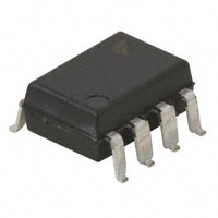
SMT 8-Pin (Lead Bend)
Tube (50 units per tube)
MID400SD
SMT 8-Pin (Lead Bend)
Tape and Reel (1,000 units per reel)
MID400V
DIP 8-Pin, DIN EN/IEC 60747-5-5 Option
Tube (50 units per tube)
MID400SV
SMT 8-Pin (Lead Bend), DIN EN/IEC 60747-5-5 Option
Tube (50 units per tube)
MID400SDV
SMT 8-Pin, DIN EN/IEC 60747-5-5 Option
Tape and Reel (1,000 units per reel)
MID400WV
DIP 8-Pin, 0.4” Lead Spacing, DIN EN/IEC 60747-5-5
Option
Tube (50 units per tube)
Marking Information
1
V
XX
3
MID400
2
YY
6
4
T1
5
Figure 10. Top Mark
Table 1. Top Mark Definitions
1
Fairchild Logo
2
Device Number
3
DIN EN/IEC60747-5-5 Option (only appears on component ordered with this option)
4
Two-Digit Year Code, e.g., “06”
5
Digit Work Week, Ranging from “01” to “53”
6
Assembly Package Code
©2005 Fairchild Semiconductor Corporation
MID400 AC Line Monitor Logic-Out Device Rev. 1.1
www.fairchildsemi.com
9
MID400 AC Line Monitor Logic-Out Device
Ordering Information
����ON Semiconductor and
are trademarks of Semiconductor Components Industries, LLC dba ON Semiconductor or its subsidiaries in the United States and/or other countries.
ON Semiconductor owns the rights to a number of patents, trademarks, copyrights, trade secrets, and other intellectual property. A listing of ON Semiconductor’s product/patent
coverage may be accessed at www.onsemi.com/site/pdf/Patent−Marking.pdf. ON Semiconductor reserves the right to make changes without further notice to any products herein.
ON Semiconductor makes no warranty, representation or guarantee regarding the suitability of its products for any particular purpose, nor does ON Semiconductor assume any liability
arising out of the application or use of any product or circuit, and specifically disclaims any and all liability, including without limitation special, consequential or incidental damages.
Buyer is responsible for its products and applications using ON Semiconductor products, including compliance with all laws, regulations and safety requirements or standards,
regardless of any support or applications information provided by ON Semiconductor. “Typical” parameters which may be provided in ON Semiconductor data sheets and/or
specifications can and do vary in different applications and actual performance may vary over time. All operating parameters, including “Typicals” must be validated for each customer
application by customer’s technical experts. ON Semiconductor does not convey any license under its patent rights nor the rights of others. ON Semiconductor products are not
designed, intended, or authorized for use as a critical component in life support systems or any FDA Class 3 medical devices or medical devices with a same or similar classification
in a foreign jurisdiction or any devices intended for implantation in the human body. Should Buyer purchase or use ON Semiconductor products for any such unintended or unauthorized
application, Buyer shall indemnify and hold ON Semiconductor and its officers, employees, subsidiaries, affiliates, and distributors harmless against all claims, costs, damages, and
expenses, and reasonable attorney fees arising out of, directly or indirectly, any claim of personal injury or death associated with such unintended or unauthorized use, even if such
claim alleges that ON Semiconductor was negligent regarding the design or manufacture of the part. ON Semiconductor is an Equal Opportunity/Affirmative Action Employer. This
literature is subject to all applicable copyright laws and is not for resale in any manner.
PUBLICATION ORDERING INFORMATION
LITERATURE FULFILLMENT:
Literature Distribution Center for ON Semiconductor
19521 E. 32nd Pkwy, Aurora, Colorado 80011 USA
Phone: 303−675−2175 or 800−344−3860 Toll Free USA/Canada
Fax: 303−675−2176 or 800−344−3867 Toll Free USA/Canada
Email: orderlit@onsemi.com
© Semiconductor Components Industries, LLC
N. American Technical Support: 800−282−9855 Toll Free
USA/Canada
Europe, Middle East and Africa Technical Support:
Phone: 421 33 790 2910
Japan Customer Focus Center
Phone: 81−3−5817−1050
www.onsemi.com
1
ON Semiconductor Website: www.onsemi.com
Order Literature: http://www.onsemi.com/orderlit
For additional information, please contact your local
Sales Representative
www.onsemi.com
�


 工商网监
湘ICP备2023018690号
工商网监
湘ICP备2023018690号
