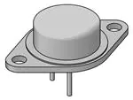
MJ15011�(NPN),
MJ15012�(PNP)
Preferred Devices
Complementary Silicon
Power Transistors
The MJ15011 and MJ15012 are PowerBase power transistors
designed for high−power audio, disk head positioners, and other linear
applications. These devices can also be used in power switching
circuits such as relay or solenoid drivers, dc−to−dc converters or
inverters.
• High Safe Operating Area (100% Tested)
1.2 A @ 100 V
• Completely Characterized for Linear Operation
• High DC Current Gain and Low Saturation Voltage
•
•
http://onsemi.com
10 AMPERE
COMPLEMENTARY
POWER TRANSISTORS
250 VOLTS
200 WATTS
hFE = 20 (Min) @ 2 A, 2 V
VCE(sat) = 2.5 V (Max) @ IC = 4 A, IB = 0.4 A
For Low Distortion Complementary Designs
Pb−Free Packages are Available*
TO−204AA (TO−3)
CASE 1−07
STYLE 1
MAXIMUM RATINGS
Rating
Symbol
Value
Unit
Collector−Emitter Voltage
VCEO
250
Vdc
Collector−Emitter Voltage
VCEX
250
Vdc
Emitter−Base Voltage
VEB
5
Vdc
Collector Current − Continuous
− Peak (Note 1)
IC
ICM
10
15
Adc
IB
Adc
Base Current − Continuous
− Peak (Note 1)
IBM
2
5
Emitter Current − Continuous
− Peak (Note 1)
IE
IEM
12
20
Adc
Total Power Dissipation @ TC = 25_C
Derate above 25_C
PD
200
1.14
Watts
W/_C
TJ, Tstg
– 65 to
+ 200
_C
Characteristic
Symbol
Max
Unit
Thermal Resistance, Junction to Case
RθJC
0.875
_C/W
TL
265
_C
Operating and Storage Junction
Temperature Range
THERMAL CHARACTERISTICS
Maximum Lead Temperature for
Soldering Purposes
Maximum ratings are those values beyond which device damage can occur.
Maximum ratings applied to the device are individual stress limit values (not
normal operating conditions) and are not valid simultaneously. If these limits are
exceeded, device functional operation is not implied, damage may occur and
reliability may be affected.
1. Pulse Test: Pulse Width = 5 ms, Duty Cycle v 10%.
*For additional information on our Pb−Free strategy and soldering details, please
download the ON Semiconductor Soldering and Mounting Techniques
Reference Manual, SOLDERRM/D.
© Semiconductor Components Industries, LLC, 2005
December, 2005 − Rev. 3
1
MARKING DIAGRAM
MJ1501xG
AYYWW
MEX
MJ1501x = Device Code
x = 1 or 2
G
= Pb−Free Package
A
= Location Code
YY
= Year
WW
= Work Week
MEX
= Country of Orgin
ORDERING INFORMATION
Device
Package
Shipping
MJ15011
TO−204AA
100 Units/Tray
MJ15011G
TO−204AA
(Pb−Free)
100 Units/Tray
MJ15012
TO−204AA
100 Units/Tray
MJ15012G
TO−204AA
(Pb−Free)
100 Units/Tray
Preferred devices are recommended choices for future use
and best overall value.
Publication Order Number:
MJ15011/D
�MJ15011 (NPN), MJ15012 (PNP)
ÎÎÎÎÎÎÎÎÎÎÎÎÎÎÎÎÎÎÎÎÎÎÎÎÎÎÎÎÎÎÎÎÎ
ÎÎÎÎÎÎÎÎÎÎÎÎÎÎÎÎÎÎÎÎÎÎ
ÎÎÎÎÎ
ÎÎÎ
ÎÎÎÎ
ÎÎÎ
ÎÎÎÎÎÎÎÎÎÎÎÎÎÎÎÎÎÎÎÎÎÎÎÎÎÎÎÎÎÎÎÎÎ
ÎÎÎÎÎÎÎÎÎÎÎÎÎÎÎÎÎÎÎÎÎÎ
ÎÎÎÎÎ
ÎÎÎ
ÎÎÎÎ
ÎÎÎ
ÎÎÎÎÎÎÎÎÎÎÎÎÎÎÎÎÎÎÎÎÎÎÎÎÎÎÎÎÎÎÎÎÎ
ÎÎÎÎÎÎÎÎÎÎÎÎÎÎÎÎÎÎÎÎÎÎ
ÎÎÎÎÎ
ÎÎÎ
ÎÎÎÎ
ÎÎÎ
ÎÎÎÎÎÎÎÎÎÎÎÎÎÎÎÎÎÎÎÎÎÎÎÎÎÎÎÎÎÎÎÎÎ
ÎÎÎÎÎÎÎÎÎÎÎÎÎÎÎÎÎÎÎÎÎÎ
ÎÎÎÎÎ
ÎÎÎ
ÎÎÎÎ
ÎÎÎ
ÎÎÎÎÎ
ÎÎÎÎÎÎÎÎÎÎÎÎÎÎÎÎÎÎÎÎÎÎ
ÎÎÎ
ÎÎÎÎ
ÎÎÎ
ÎÎÎÎÎÎÎÎÎÎÎÎÎÎÎÎÎÎÎÎÎÎ
ÎÎÎÎÎ
ÎÎÎ
ÎÎÎÎ
ÎÎÎ
ÎÎÎÎÎÎÎÎÎÎÎÎÎÎÎÎÎÎÎÎÎÎ
ÎÎÎÎÎ
ÎÎÎ
ÎÎÎÎ
ÎÎÎ
ÎÎÎÎÎÎÎÎÎÎÎÎÎÎÎÎÎÎÎÎÎÎ
ÎÎÎ
ÎÎÎÎ
ÎÎÎ
ÎÎÎÎÎ
ÎÎÎÎÎÎÎÎÎÎÎÎÎÎÎÎÎÎÎÎÎÎ
ÎÎÎÎÎ
ÎÎÎ
ÎÎÎÎ
ÎÎÎ
ÎÎÎÎÎÎÎÎÎÎÎÎÎÎÎÎÎÎÎÎÎÎÎÎÎÎÎÎÎÎÎÎÎ
ÎÎÎÎÎÎÎÎÎÎÎÎÎÎÎÎÎÎÎÎÎÎ
ÎÎÎÎÎ
ÎÎÎ
ÎÎÎÎ
ÎÎÎ
ÎÎÎÎÎÎÎÎÎÎÎÎÎÎÎÎÎÎÎÎÎÎ
ÎÎÎÎÎ
ÎÎÎ
ÎÎÎÎ
ÎÎÎ
ÎÎÎÎÎÎÎÎÎÎÎÎÎÎÎÎÎÎÎÎÎÎÎÎÎÎÎÎÎÎÎÎÎ
ÎÎÎÎÎÎÎÎÎÎÎÎÎÎÎÎÎÎÎÎÎÎ
ÎÎÎÎÎ
ÎÎÎ
ÎÎÎÎ
ÎÎÎ
ÎÎÎÎÎ
ÎÎÎÎÎÎÎÎÎÎÎÎÎÎÎÎÎÎÎÎÎÎ
ÎÎÎ
ÎÎÎÎ
ÎÎÎ
ÎÎÎÎÎÎÎÎÎÎÎÎÎÎÎÎÎÎÎÎÎÎ
ÎÎÎÎÎ
ÎÎÎ
ÎÎÎÎ
ÎÎÎ
ÎÎÎÎÎÎÎÎÎÎÎÎÎÎÎÎÎÎÎÎÎÎ
ÎÎÎÎÎ
ÎÎÎ
ÎÎÎÎ
ÎÎÎ
ÎÎÎÎÎÎÎÎÎÎÎÎÎÎÎÎÎÎÎÎÎÎ
ÎÎÎÎ
ÎÎÎ
ÎÎÎÎÎ
ÎÎÎ
ÎÎÎÎÎÎÎÎÎÎÎÎÎÎÎÎÎÎÎÎÎÎ
ÎÎÎÎÎÎÎÎÎÎÎÎÎÎÎÎÎÎÎÎÎÎÎÎÎÎÎÎÎÎÎÎÎ
ÎÎÎÎÎ
ÎÎÎ
ÎÎÎÎ
ÎÎÎ
ÎÎÎÎÎÎÎÎÎÎÎÎÎÎÎÎÎÎÎÎÎÎÎÎÎÎÎÎÎÎÎÎÎ
ÎÎÎÎÎÎÎÎÎÎÎÎÎÎÎÎÎÎÎÎÎÎ
ÎÎÎÎÎ
ÎÎÎ
ÎÎÎÎ
ÎÎÎ
ÎÎÎÎÎÎÎÎÎÎÎÎÎÎÎÎÎÎÎÎÎÎ
ÎÎÎÎÎ
ÎÎÎ
ÎÎÎÎ
ÎÎÎ
ÎÎÎÎÎÎÎÎÎÎÎÎÎÎÎÎÎÎÎÎÎÎÎÎÎÎÎÎÎÎÎÎÎ
ÎÎÎÎÎÎÎÎÎÎÎÎÎÎÎÎÎÎÎÎÎÎ
ÎÎÎÎÎ
ÎÎÎ
ÎÎÎÎ
ÎÎÎ
ÎÎÎÎÎÎÎÎÎÎÎÎÎÎÎÎÎÎÎÎÎÎÎÎÎÎÎÎÎÎÎÎÎ
ÎÎÎÎÎÎÎÎÎÎÎÎÎÎÎÎÎÎÎÎÎÎ
ÎÎÎÎÎ
ÎÎÎ
ÎÎÎÎ
ÎÎÎ
ÎÎÎÎÎÎÎÎÎÎÎÎÎÎÎÎÎÎÎÎÎÎ
ÎÎÎÎÎ
ÎÎÎ
ÎÎÎÎ
ÎÎÎ
ÎÎÎÎÎÎÎÎÎÎÎÎÎÎÎÎÎÎÎÎÎÎ
ÎÎÎÎÎ
ÎÎÎÎÎÎÎÎÎÎ
ELECTRICAL CHARACTERISTICS (TC = 25_C unless otherwise noted)
Characteristic
Symbol
Min
Max
Unit
V(BR)CEO
250
−
Vdc
Collector Cutoff Current
(VCE = 200 Vdc)
ICEO
−
1
mAdc
Collector Cutoff Current
(VCE = 250 Vdc, VBE(off) = 15 Vdc)
ICEX
−
100
μAdc
Emitter Cutoff Current
(VBE = 5 Vdc)
IEBO
−
10
μAdc
20
15
120
−
−
−
0.6
1.0
OFF CHARACTERISTICS
Collector−Emitter Breakdown Voltage (Note 2)
(IC = 100 mA)
ON CHARACTERISTICS (Note 2)
DC Current Gain
(IC = 2 Adc, VCE = 2 Vdc)
(IC = 4 Adc, VCE = 2 Vdc)
hFE
−
Collector−Emitter Saturation Voltage
(IC = 2 Adc, IB = 0.2 Adc)
(IC = 4 Adc, IB = 0.4 Adc)
VCE(sat)
Vdc
Base−Emitter On Voltage
(IC = 4 Adc, VCE = 2 Vdc)
VBE(on)
−
1.8
Vdc
Cob
−
750
pF
5
1.4
−
−
DYNAMIC CHARACTERISTICS
Output Capacitance
(VCB = 10 Vdc, f = 1 MHz)
SECOND BREAKDOWN
Second Breakdown Collector Current with Base Forward Biased
(VCE = 40 Vdc, t = 0.5 s)
(VCE = 100 Vdc, t = 0.5 s)
IS/b
Adc
2. Pulse Test: Pulse Width = 300 μs, Duty Cycle v 2%.
200
10
hFE , DC CURRENT GAIN
100
IC, COLLECTOR CURRENT (AMP)
VCE = 2 Vdc
50
20
MJ15011
MJ15012
10
5
2
dc
1
0.5
5
BONDING WIRE LIMIT
THERMAL LIMIT @ TC = 25°C
(SINGLE PULSE)
SECOND BREAKDOWN LIMIT
0.2
2
0.1
0.2
0.5
1
2
IC, COLLECTOR CURRENT
5
0.1
15
10
Figure 1. DC Current Gain
20
30
50
70
100
150 200
VCE, COLLECTOR−EMITTER VOLTAGE (VOLTS)
Figure 2. Active Region Safe Operating Area
http://onsemi.com
2
300
�MJ15011 (NPN), MJ15012 (PNP)
PACKAGE DIMENSIONS
TO−204 (TO−3)
CASE 1−07
ISSUE Z
NOTES:
1. DIMENSIONING AND TOLERANCING PER ANSI
Y14.5M, 1982.
2. CONTROLLING DIMENSION: INCH.
3. ALL RULES AND NOTES ASSOCIATED WITH
REFERENCED TO−204AA OUTLINE SHALL APPLY.
A
N
C
−T−
E
D
K
2 PL
0.13 (0.005)
U
T Q
M
M
Y
DIM
A
B
C
D
E
G
H
K
L
N
Q
U
V
M
−Y−
L
V
SEATING
PLANE
2
H
G
B
M
T Y
1
−Q−
0.13 (0.005)
INCHES
MIN
MAX
1.550 REF
−−− 1.050
0.250
0.335
0.038
0.043
0.055
0.070
0.430 BSC
0.215 BSC
0.440
0.480
0.665 BSC
−−− 0.830
0.151
0.165
1.187 BSC
0.131
0.188
STYLE 1:
PIN 1. BASE
2. EMITTER
CASE: COLLECTOR
M
http://onsemi.com
3
MILLIMETERS
MIN
MAX
39.37 REF
−−− 26.67
6.35
8.51
0.97
1.09
1.40
1.77
10.92 BSC
5.46 BSC
11.18
12.19
16.89 BSC
−−− 21.08
3.84
4.19
30.15 BSC
3.33
4.77
�MECHANICAL CASE OUTLINE
PACKAGE DIMENSIONS
TO−204 (TO−3)
CASE 1−07
ISSUE Z
DATE 05/18/1988
SCALE 1:1
A
N
NOTES:
1. DIMENSIONING AND TOLERANCING PER ANSI
Y14.5M, 1982.
2. CONTROLLING DIMENSION: INCH.
3. ALL RULES AND NOTES ASSOCIATED WITH
REFERENCED TO-204AA OUTLINE SHALL APPLY.
C
−T−
E
D
K
2 PL
0.13 (0.005)
U
T Q
M
M
Y
DIM
A
B
C
D
E
G
H
K
L
N
Q
U
V
M
−Y−
L
V
SEATING
PLANE
2
H
G
B
M
T Y
1
−Q−
0.13 (0.005)
INCHES
MIN
MAX
1.550 REF
--1.050
0.250
0.335
0.038
0.043
0.055
0.070
0.430 BSC
0.215 BSC
0.440
0.480
0.665 BSC
--0.830
0.151
0.165
1.187 BSC
0.131
0.188
MILLIMETERS
MIN
MAX
39.37 REF
--26.67
6.35
8.51
0.97
1.09
1.40
1.77
10.92 BSC
5.46 BSC
11.18
12.19
16.89 BSC
--21.08
3.84
4.19
30.15 BSC
3.33
4.77
M
STYLE 1:
PIN 1. BASE
2. EMITTER
CASE: COLLECTOR
STYLE 2:
PIN 1. BASE
2. COLLECTOR
CASE: EMITTER
STYLE 3:
PIN 1. GATE
2. SOURCE
CASE: DRAIN
STYLE 4:
PIN 1. GROUND
2. INPUT
CASE: OUTPUT
STYLE 6:
PIN 1. GATE
2. EMITTER
CASE: COLLECTOR
STYLE 7:
PIN 1. ANODE
2. OPEN
CASE: CATHODE
STYLE 8:
PIN 1. CATHODE #1
2. CATHODE #2
CASE: ANODE
STYLE 9:
PIN 1. ANODE #1
2. ANODE #2
CASE: CATHODE
STYLE 5:
PIN 1. CATHODE
2. EXTERNAL TRIP/DELAY
CASE: ANODE
ON Semiconductor and
are trademarks of Semiconductor Components Industries, LLC (SCILLC). SCILLC reserves the right to make changes
without further notice to any products herein. SCILLC makes no warranty, representation or guarantee regarding the suitability of its products for any particular
purpose, nor does SCILLC assume any liability arising out of the application or use of any product or circuit, and specifically disclaims any and all liability,
including without limitation special, consequential or incidental damages. “Typical” parameters which may be provided in SCILLC data sheets and/or
specifications can and do vary in different applications and actual performance may vary over time. All operating parameters, including “Typicals” must be
validated for each customer application by customer’s technical experts. SCILLC does not convey any license under its patent rights nor the rights of others.
SCILLC products are not designed, intended, or authorized for use as components in systems intended for surgical implant into the body, or other applications
intended to support or sustain life, or for any other application in which the failure of the SCILLC product could create a situation where personal injury or
death may occur. Should Buyer purchase or use SCILLC products for any such unintended or unauthorized application, Buyer shall indemnify and hold
SCILLC and its officers, employees, subsidiaries, affiliates, and distributors harmless against all claims, costs, damages, and expenses, and reasonable
attorney fees arising out of, directly or indirectly, any claim of personal injury or death associated with such unintended or unauthorized use, even if such claim
alleges that SCILLC was negligent regarding the design or manufacture of the part. SCILLC is an Equal Opportunity/Affirmative Action Employer.
© Semiconductor Components Industries, LLC, 2000
January, 2000 − Rev. 07Z
1
Case Outline Number:
1
�onsemi,
, and other names, marks, and brands are registered and/or common law trademarks of Semiconductor Components Industries, LLC dba “onsemi” or its affiliates
and/or subsidiaries in the United States and/or other countries. onsemi owns the rights to a number of patents, trademarks, copyrights, trade secrets, and other intellectual property.
A listing of onsemi’s product/patent coverage may be accessed at www.onsemi.com/site/pdf/Patent−Marking.pdf. onsemi reserves the right to make changes at any time to any
products or information herein, without notice. The information herein is provided “as−is” and onsemi makes no warranty, representation or guarantee regarding the accuracy of the
information, product features, availability, functionality, or suitability of its products for any particular purpose, nor does onsemi assume any liability arising out of the application or use
of any product or circuit, and specifically disclaims any and all liability, including without limitation special, consequential or incidental damages. Buyer is responsible for its products
and applications using onsemi products, including compliance with all laws, regulations and safety requirements or standards, regardless of any support or applications information
provided by onsemi. “Typical” parameters which may be provided in onsemi data sheets and/or specifications can and do vary in different applications and actual performance may
vary over time. All operating parameters, including “Typicals” must be validated for each customer application by customer’s technical experts. onsemi does not convey any license
under any of its intellectual property rights nor the rights of others. onsemi products are not designed, intended, or authorized for use as a critical component in life support systems
or any FDA Class 3 medical devices or medical devices with a same or similar classification in a foreign jurisdiction or any devices intended for implantation in the human body. Should
Buyer purchase or use onsemi products for any such unintended or unauthorized application, Buyer shall indemnify and hold onsemi and its officers, employees, subsidiaries, affiliates,
and distributors harmless against all claims, costs, damages, and expenses, and reasonable attorney fees arising out of, directly or indirectly, any claim of personal injury or death
associated with such unintended or unauthorized use, even if such claim alleges that onsemi was negligent regarding the design or manufacture of the part. onsemi is an Equal
Opportunity/Affirmative Action Employer. This literature is subject to all applicable copyright laws and is not for resale in any manner.
PUBLICATION ORDERING INFORMATION
LITERATURE FULFILLMENT:
Email Requests to: orderlit@onsemi.com
onsemi Website: www.onsemi.com
◊
TECHNICAL SUPPORT
North American Technical Support:
Voice Mail: 1 800−282−9855 Toll Free USA/Canada
Phone: 011 421 33 790 2910
Europe, Middle East and Africa Technical Support:
Phone: 00421 33 790 2910
For additional information, please contact your local Sales Representative
�