MJF31C (NPN),
MJF32C (PNP)
Preferred Device
Complementary Silicon
Plastic Power Transistors
for Isolated Package
Applications
http://onsemi.com
Designed for use in general purpose amplifier and switching
applications.
Features
• Collector−Emitter Saturation Voltage −
•
•
•
•
3.0 AMPERE
POWER TRANSISTORS
COMPLEMENTARY SILICON
100 VOLTS, 28 WATTS
VCE(sat) = 1.2 Vdc (Max) @ IC = 3.0 Adc
Collector−Emitter Sustaining Voltage −
VCEO(sus) = 100 Vdc (Min)
High Current Gain − Bandwidth Product
fT = 3.0 MHz (Min) @ IC = 500 mAdc
UL Recognized, File #E69369, to 3500 VRMS Isolation
Pb−Free Packages are Available*
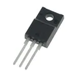
4
TO−220 FULLPAK
CASE 221D
STYLE 2
ÎÎÎÎÎÎÎÎÎÎÎÎÎÎÎÎÎÎÎ
ÎÎÎÎÎÎÎÎÎÎÎÎÎÎÎÎÎÎÎ
ÎÎÎÎÎÎÎÎÎÎÎÎ
ÎÎÎ
ÎÎÎÎ
ÎÎÎ
ÎÎÎÎÎÎÎÎÎÎÎÎ
ÎÎÎ
ÎÎÎÎ
ÎÎÎ
ÎÎÎÎÎÎÎÎÎÎÎÎ
ÎÎÎ
ÎÎÎÎ
ÎÎÎ
ÎÎÎÎÎÎÎÎÎÎÎÎ
ÎÎÎ
ÎÎÎÎ
ÎÎÎ
ÎÎÎÎÎÎÎÎÎÎÎÎ
ÎÎÎ
ÎÎÎÎ
ÎÎÎ
ÎÎÎÎÎÎÎÎÎÎÎÎ
ÎÎÎ
ÎÎÎÎ
ÎÎÎ
ÎÎÎÎÎÎÎÎÎÎÎÎ
ÎÎÎ
ÎÎÎÎ
ÎÎÎ
ÎÎÎÎÎÎÎÎÎÎÎÎ
ÎÎÎ
ÎÎÎÎ
ÎÎÎ
ÎÎÎÎÎÎÎÎÎÎÎÎ
ÎÎÎ
ÎÎÎÎ
ÎÎÎ
ÎÎÎÎÎÎÎÎÎÎÎÎ
ÎÎÎ
ÎÎÎÎ
ÎÎÎ
ÎÎÎÎÎÎÎÎÎÎÎÎ
ÎÎÎ
ÎÎÎÎ
ÎÎÎ
ÎÎÎÎÎÎÎÎÎÎÎÎ
ÎÎÎ
ÎÎÎÎ
ÎÎÎ
ÎÎÎÎÎÎÎÎÎÎÎÎ
ÎÎÎ
ÎÎÎÎ
ÎÎÎ
ÎÎÎÎÎÎÎÎÎÎÎÎ
ÎÎÎ
ÎÎÎÎ
ÎÎÎ
1
MAXIMUM RATINGS
Rating
Symbol
Value
Unit
VCEO
100
Vdc
Collector−Base Voltage
VCB
100
Vdc
Emitter−Base Voltage
VEB
5.0
Vdc
Collector−Emitter Voltage
Collector CurrentUnclamped Inductive
Load Energy (Note 1)
− Continuous
− Peak
IC
Base Current
IB
1.0
Adc
Total Power Dissipation @ TC = 25_C
Derate above 25_C
PD
28
0.22
W
W/_C
Total Power Dissipation @ TA = 25_C
Derate above 25_C
PD
2.0
0.016
W
W/_C
Unclamped Inductive Load Energy (Note 1)
E
32
mJ
–65 to +150
_C
MARKING DIAGRAM
Characteristic
Symbol
Max
Unit
Thermal Resistance, Junction−to−Ambient
RqJC
62.5
°C/W
Thermal Resistance, Junction−to−Case
RqJC
4.46
°C/W
MJF3xCG
AYWW
x
G
A
Y
WW
THERMAL CHARACTERISTICS
Maximum ratings are those values beyond which device damage can occur.
Maximum ratings applied to the device are individual stress limit values (not
normal operating conditions) and are not valid simultaneously. If these limits are
exceeded, device functional operation is not implied, damage may occur and
reliability may be affected.
1. IC = 1.8 A, L = 20 mH, P.R.F. = 10 Hz, VCC = 10 V, RBE = 100 W.
*For additional information on our Pb−Free strategy and soldering details, please
download the ON Semiconductor Soldering and Mounting Techniques
Reference Manual, SOLDERRM/D.
© Semiconductor Components Industries, LLC, 2008
July, 2008 − Rev. 5
3
Adc
3.0
5.0
TJ, Tstg
Operating and Storage Junction
Temperature Range
2
1
= 1 or 2
= Pb−Free Package
= Assembly Location
= Year
= Work Week
ORDERING INFORMATION
Device
Package
Shipping
MJF31C
TO−220 FULLPAK
50 Units/Rail
MJF31CG
TO−220 FULLPAK
(Pb−Free)
50 Units/Rail
MJF32C
TO−220 FULLPAK
50 Units/Rail
MJF32CG
TO−220 FULLPAK
(Pb−Free)
50 Units/Rail
Preferred devices are recommended choices for future use
and best overall value.
Publication Order Number:
MJF31C/D
�MJF31C (NPN), MJF32C (PNP)
ÎÎÎÎÎÎÎÎÎÎÎÎÎÎÎÎÎÎÎÎÎÎÎÎÎÎÎÎÎÎÎÎÎ
ÎÎÎÎÎÎÎÎÎÎÎÎÎÎÎÎÎÎÎÎÎÎ
ÎÎÎÎÎ
ÎÎÎ
ÎÎÎÎ
ÎÎÎ
ÎÎÎÎÎÎÎÎÎÎÎÎÎÎÎÎÎÎÎÎÎÎÎÎÎÎÎÎÎÎÎÎÎ
ÎÎÎÎÎÎÎÎÎÎÎÎÎÎÎÎÎÎÎÎÎÎ
ÎÎÎÎÎ
ÎÎÎ
ÎÎÎÎ
ÎÎÎ
ÎÎÎÎÎÎÎÎÎÎÎÎÎÎÎÎÎÎÎÎÎÎÎÎÎÎÎÎÎÎÎÎÎ
ÎÎÎÎÎÎÎÎÎÎÎÎÎÎÎÎÎÎÎÎÎÎ
ÎÎÎÎÎ
ÎÎÎ
ÎÎÎÎ
ÎÎÎ
ÎÎÎÎÎÎÎÎÎÎÎÎÎÎÎÎÎÎÎÎÎÎÎÎÎÎÎÎÎÎÎÎÎ
ÎÎÎÎÎÎÎÎÎÎÎÎÎÎÎÎÎÎÎÎÎÎ
ÎÎÎÎÎ
ÎÎÎ
ÎÎÎÎ
ÎÎÎ
ÎÎÎÎÎÎÎÎÎÎÎÎÎÎÎÎÎÎÎÎÎÎ
ÎÎÎÎÎ
ÎÎÎ
ÎÎÎÎ
ÎÎÎ
ÎÎÎÎÎÎÎÎÎÎÎÎÎÎÎÎÎÎÎÎÎÎ
ÎÎÎÎÎ
ÎÎÎ
ÎÎÎÎ
ÎÎÎ
ÎÎÎÎÎÎÎÎÎÎÎÎÎÎÎÎÎÎÎÎÎÎ
ÎÎÎÎÎ
ÎÎÎ
ÎÎÎÎ
ÎÎÎ
ÎÎÎÎÎÎÎÎÎÎÎÎÎÎÎÎÎÎÎÎÎÎÎÎÎÎÎÎÎÎÎÎÎ
ÎÎÎÎÎÎÎÎÎÎÎÎÎÎÎÎÎÎÎÎÎÎ
ÎÎÎÎÎ
ÎÎÎ
ÎÎÎÎ
ÎÎÎ
ÎÎÎÎÎÎÎÎÎÎÎÎÎÎÎÎÎÎÎÎÎÎÎÎÎÎÎÎÎÎÎÎÎ
ÎÎÎÎÎÎÎÎÎÎÎÎÎÎÎÎÎÎÎÎÎÎ
ÎÎÎÎÎ
ÎÎÎ
ÎÎÎÎ
ÎÎÎ
ÎÎÎÎÎÎÎÎÎÎÎÎÎÎÎÎÎÎÎÎÎÎ
ÎÎÎÎÎ
ÎÎÎ
ÎÎÎÎ
ÎÎÎ
ÎÎÎÎÎÎÎÎÎÎÎÎÎÎÎÎÎÎÎÎÎÎ
ÎÎÎÎÎ
ÎÎÎ
ÎÎÎÎ
ÎÎÎ
ÎÎÎÎÎÎÎÎÎÎÎÎÎÎÎÎÎÎÎÎÎÎ
ÎÎÎÎÎÎÎÎÎÎÎÎÎÎÎÎÎÎÎÎÎÎÎÎÎÎÎÎÎÎÎÎÎ
ÎÎÎÎÎ
ÎÎÎ
ÎÎÎÎ
ÎÎÎ
ÎÎÎÎÎÎÎÎÎÎÎÎÎÎÎÎÎÎÎÎÎÎÎÎÎÎÎÎÎÎÎÎÎ
ÎÎÎÎÎÎÎÎÎÎÎÎÎÎÎÎÎÎÎÎÎÎ
ÎÎÎÎÎ
ÎÎÎ
ÎÎÎÎ
ÎÎÎ
ÎÎÎÎÎÎÎÎÎÎÎÎÎÎÎÎÎÎÎÎÎÎ
ÎÎÎÎÎ
ÎÎÎ
ÎÎÎÎ
ÎÎÎ
ÎÎÎÎÎÎÎÎÎÎÎÎÎÎÎÎÎÎÎÎÎÎ
ÎÎÎÎÎ
ÎÎÎ
ÎÎÎÎ
ÎÎÎ
ELECTRICAL CHARACTERISTICS (TC = 25_C unless otherwise noted)
Characteristic
Symbol
Min
Max
100
−
−
0.3
Unit
OFF CHARACTERISTICS
Collector−Emitter Sustaining Voltage (Note 2)
(IC = 30 mAdc, IB = 0)
VCEO(sus)
Vdc
Collector Cutoff Current
(IC = 3.0 Adc, VCE = 4.0 Vdc)
ICEO
mAdc
Collector Cutoff Current
ICES
−
200
mAdc
Emitter Cutoff Current (VBE = 5.0 Vdc, IC = 0)
IEBO
−
1.0
mAdc
hFE
25
10
−
50
−
Collector−Emitter Saturation Voltage (IC = 3.0 Adc, IB = 375 mAdc)
VCE(sat)
−
1.2
Vdc
Base−Emitter On Voltage (IC = 3.0 Adc, VCE = 4.0 Vdc)
VBE(on)
−
1.8
Vdc
Current−Gain − Bandwidth Product (IC = 500 mAdc, VCE = 10 Vdc, ftest = 1.0 MHz)
fT
3.0
−
MHz
Small−Signal Current Gain (IC = 0.5 Adc, VCE = 10 Vdc, f = 1.0 kHz)
hfe
20
−
−
ON CHARACTERISTICS (Note 2)
DC Current Gain (IC = 1.0 Adc, VCE = 4.0 Vdc)
(IC = 3.0 Adc, VCE = 4.0 Vdc)
DYNAMIC CHARACTERISTICS
2. Pulse Test: Pulse Width v 300 ms, Duty Cycle v 2.0%.
P D, POWER DISSIPATION (WATTS)
TC TA
40 4.0
30 3.0
TC
20 2.0
TA
10 1.0
0
0
0
20
40
60
100
120
80
T, TEMPERATURE (°C)
140
160
Figure 1. Power Derating
TURN-ON PULSE
APPROX
+11 V
VCC
2.0
RC
IC/IB = 10
TJ = 25°C
1.0
VEB(off)
SCOPE
Vin
Vin 0
0.7
0.5
RB
t3
APPROX
+11 V
Cjd
很抱歉,暂时无法提供与“MJF31CG”相匹配的价格&库存,您可以联系我们找货
免费人工找货- 国内价格
- 1+9.64780
- 10+8.20060
- 50+6.75350
- 100+6.02990
- 500+5.54750
- 1000+4.82390
- 国内价格
- 1+3.21117
- 10+1.87046
- 50+0.94349
- 100+0.81432
- 500+0.75816
- 1000+0.73149
- 国内价格
- 1+14.21669
- 5+11.32400
- 10+9.45543
- 50+5.77459
- 100+5.41765
- 国内价格
- 5+13.12769
- 15+12.73821
- 25+12.35706