MJF47G
High Voltage Power
Transistor
Isolated Package Applications
Designed for line operated audio output amplifiers, switching power
supply drivers and other switching applications, where the mounting
surface of the device is required to be electrically isolated from the
heatsink or chassis.
Features
•
•
•
•
•
•
•
Electrically Similar to the Popular TIP47
250 VCEO(sus)
1 A Rated Collector Current
No Isolating Washers Required
Reduced System Cost
UL Recognized, File #E69369, to 3500 VRMS Isolation
This is a Pb−Free Device*
http://onsemi.com
NPN SILICON
POWER TRANSISTOR
1 AMPERE
250 VOLTS, 28 WATTS
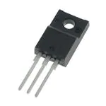
TO−220 FULLPACK
CASE 221D
STYLE 2
MAXIMUM RATINGS
Rating
Symbol
Value
Unit
VCEO
250
Vdc
Collector−Base Voltage
VCB
350
Vdc
Emitter−Base Voltage
VEB
5
Vdc
Collector−Emitter Voltage
RMS Isolation Voltage (Note 1)
Test No. 1 Per Figure 10
Test No. 2 Per Figure 11
Test No. 3 Per Figure 12
(for 1 sec, R.H. < 30%, TA = 25_C)
Collector Current
− Continuous
− Peak
VISOL
4500
3500
1500
1
2
Adc
Base Current − Continuous
IB
0.6
Adc
Total Power Dissipation (Note 2) @ TC = 25_C
Derate above 25_C
PD
28.4
0.227
W
W/_C
Total Power Dissipation @ TA = 25_C
Derate above 25_C
PD
2.0
0.016
W
W/_C
TJ, Tstg
–65 to +150
_C
Characteristic
Symbol
Max
Unit
RqJA
62.5
_C/W
Thermal Resistance, Junction−to−Case (Note 2)
RqJC
4.4
_C/W
Lead Temperature for Soldering Purposes
TL
260
_C
Stresses exceeding Maximum Ratings may damage the device. Maximum
Ratings are stress ratings only. Functional operation above the Recommended
Operating Conditions is not implied. Extended exposure to stresses above the
Recommended Operating Conditions may affect device reliability.
1. Proper strike and creepage distance must be provided.
2. Measurement made with thermocouple contacting the bottom insulated
surface (in a location beneath the die), the devices mounted on a heatsink with
thermal grease and a mounting torque of ≥ 6 in. lbs.
*For additional information on our Pb−Free strategy and soldering details, please
download the ON Semiconductor Soldering and Mounting Techniques
Reference Manual, SOLDERRM/D.
© Semiconductor Components Industries, LLC, 2012
October, 2012 − Rev. 6
1
3
MJF47G
AYWW
G
A
Y
WW
THERMAL CHARACTERISTICS
Thermal Resistance, Junction−to−Ambient
2
MARKING DIAGRAM
V
IC
Operating and Storage Temperature Range
1
= Pb−Free Package
= Assembly Location
= Year
= Work Week
ORDERING INFORMATION
Device
MJF47G
Package
Shipping
TO−220 FULLPACK
(Pb−Free)
50 Units/Rail
*For additional information on our Pb−Free strategy
and soldering details, please download the
ON Semiconductor Soldering and Mounting
Techniques Reference Manual, SOLDERRM/D.
Publication Order Number:
MJF47/D
�MJF47G
ELECTRICAL CHARACTERISTICS (TC = 25_C unless otherwise noted)
Symbol
Min
Max
Unit
VCEO(sus)
250
−
Vdc
Collector Cutoff Current
(VCE = 150 Vdc, IB = 0)
ICEO
−
0.2
mAdc
Collector Cutoff Current
(VCE = 350 Vdc, VBE = 0)
ICES
−
0.1
mAdc
Emitter Cutoff Current
(VBE = 5 Vdc, IC = 0)
IEBO
−
1
mAdc
30
10
150
−
Characteristic
OFF CHARACTERISTICS
Collector−Emitter Sustaining Voltage (Note 3)
(IC = 30 mAdc, IB = 0)
ON CHARACTERISTICS (Note 3)
hFE
DC Current Gain
(IC = 0.3 Adc, VCE = 10 Vdc)
(IC = 1 Adc, VCE = 10 Vdc)
−
Collector−Emitter Saturation Voltage
(IC = 1 Adc, IB = 0.2 Adc)
VCE(sat)
−
1
Vdc
Base−Emitter On Voltage
(IC = 1 Adc, VCE = 10 Vdc)
VBE(on)
−
1.5
Vdc
fT
10
−
MHz
DYNAMIC CHARACTERISTICS
Current Gain − Bandwidth Product
(IC = 0.2 Adc, VCE 10 Vdc, f = 2 MHz)
3. Pulse Test: Pulse Width v 300 ms, Duty Cycle v 2%.
TYPICAL CHARACTERISTICS
200
1.4
VCE = 10 V
1.2
60
40
TJ = 150°C
V, VOLTAGE (VOLTS)
hFE , DC CURRENT GAIN
100
25°C
20
-�55°C
10
6
4
2
0.02
1
0.8
0.6
VBE(on) @ VCE = 4 V
0.4
TJ = 25°C
0.2
0.04 0.06 0.1
0.2
0.4 0.6
IC, COLLECTOR CURRENT (AMPS)
1
0
0.02
2
VBE(sat) @ IC/IB = 5
Figure 1. DC Current Gain
VCE(sat) @ IC/IB = 5 V
0.04 0.06
0.1
0.2
0.4 0.6
IC, COLLECTOR CURRENT (AMPS)
Figure 2. “On” Voltages
http://onsemi.com
2
1
2
�MJF47G
1
5
TJ = 25°C
VCC = 200 V
IC/IB = 5
tr
2
0.2
t, TIME (��s)
μ
t, TIME (��s)
μ
0.5
td
0.1
0.05
1
0.5
tf
0.2
0.1
0.02
0.01
0.02
TJ = 25°C
VCC = 200 V
IC/IB = 5
ts
0.05
0.2
0.5
0.1
IC, COLLECTOR CURRENT (AMPS)
1
0.05
0.02
2
0.05
Figure 3. Turn−On Time
0.1
0.2
0.5
IC, COLLECTOR CURRENT (AMPS)
1
2
Figure 4. Turn−Off Time
TURN-ON PULSE
APPROX
+11 V
VCC
RC
SCOPE
Vin
Vin 0
VEB(off)
RB
51
t1
Cjd
很抱歉,暂时无法提供与“MJF47”相匹配的价格&库存,您可以联系我们找货
免费人工找货