Revised February 2002
MM74C906 • MM74C907
Hex Open Drain N-Channel Buffers •
Hex Open Drain P-Channel Buffers
General Description
Features
The MM74C906 and MM74C907 buffers employ monolithic
CMOS technology in achieving open drain outputs. The
MM74C906 consists of six inverters driving six N-channel
devices; and the MM74C907 consists of six inverters driving six P-channel devices. The open drain feature of these
buffers makes level shifting or wire AND and wire OR functions by just the addition of pull-up or pull-down resistors.
All inputs are protected from static discharge by diode
clamps to VCC and to ground.
■ Wide supply voltage range:
3V to 15V
■ Guaranteed noise margin: 1V
■ High noise immunity: 0.45 VCC (typ.)
■ High current sourcing and sinking open drain outputs
Ordering Code:
Order Number
Package Number
Package Description
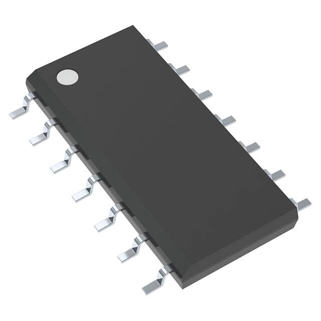
MM74C906M
M14A
14-Lead Small Outline Integrated Circuit (SOIC), JEDEC MS-012, 0.150" Narrow
MM74C906N
N14A
14-Lead Plastic Dual-In-Line Package (PDIP), JEDEC MS-001, 0.300" Wide
MM74C907N
N14A
14-Lead Plastic Dual-In-Line Package (PDIP), JEDEC MS-001, 0.300" Wide
Devices also available in Tape and Reel. Specify by appending the suffix letter “X” to the ordering code.
Connection Diagram
Logic Diagrams
Pin Assignments for DIP and SOIC
MM74C906
MM74C907
Top View
© 2002 Fairchild Semiconductor Corporation
DS005911
www.fairchildsemi.com
MM74C906 • MM74C907 Hex Open Drain N-Channel Buffers • Hex Open Drain P-Channel Buffers
October 1987
�MM74C906 • MM74C907
Absolute Maximum Ratings(Note 1)
Voltage at Any Input Pin
Operating VCC Range
3V to 15V
18V
Absolute Maximum VCC
−0.3V to VCC +0.3V
Lead Temperature (TL)
Voltage at Any Output Pin
260°C
(Soldering, 10 seconds)
Operating Temperature Range
MM74C906/MM74C907
−40°C to +85°C
Storage Temperature Range
−65°C to +150 °C
Note 1: “Absolute Maximum Ratings” are those values beyond which the
safety of the device cannot be guaranteed. Except for “Operating Temperature Range” they are not meant to imply that the devices should be operated at these limits. The table of “Electrical Characteristics” provides
conditions for actual device operation.
Power Dissipation
Dual-In-Line
700 mW
Small Outline
500 mW
DC Electrical Characteristics
Min/Max limits apply across temperature range unless otherwise noted
Symbol
Parameter
Conditions
Min
Typ
Max
Units
CMOS TO CMOS
VIN(1)
VIN(0)
Logical “1” Input Voltage
Logical “0” Input Voltage
VCC = 5V
3.5
V
VCC = 10V
8.0
V
VCC = 5V
1.5
V
VCC = 10V
2
V
1
µA
IIN(1)
Logical “1” Input Current
VCC = 15V, VIN = 15V
IIN(0)
Logical “0” Input Current
VCC = 15V, VIN = 0V
ICC
Supply Current
VCC = 15V, Output Open
0.05
15
µA
VCC = 4.75V, VIN = VCC − 1.5V
0.005
5
µA
0.005
5
µA
0.8
V
0.005
−1.0
−0.005
µA
Output Leakage
MM74C906
VCC = 4.75V, VOUT = 18V
MM74C907
VCC = 4.75V, VIN = 1V + 0.1 VCC
VCC = 4.75V, VOUT = VCC − 18V
CMOS/LPTTL INTERFACE
VIN(1)
Logical “1” Input Voltage
VCC = 4.75V
VIN(0)
Logical “0” Input Voltage
VCC = 4.75V
VCC − 1.5V
V
OUTPUT DRIVE CURRENT
MM74C906
MM74C907
MM74C906
MM74C907
www.fairchildsemi.com
VCC = 4.75V, VIN = 1V + 0.1 VCC
VCC = 4.75V, VOUT = 0.5V
2.1
8.0
mA
VCC = 4.75V, VOUT = 1.0V
4.2
12.0
mA
VCC = 4.75V, VOUT = VCC − 0.5V
−1.05
−1.5
mA
VCC = 4.75V, VOUT = VCC − 1V
−2.1
−3.0
mA
VCC = 10V, VOUT = 0.5V
4.2
20
mA
VCC = 10V, VOUT = 1V
8.4
30
mA
VCC = 10V, VOUT = 9.5V
−2.1
−4.0
mA
VCC = 10V, VOUT = 9V
−4.2
−8.0
mA
VCC = 4.75V, VIN = VCC − 1.5V
VCC = 10V, VIN = 2V
VCC = 10V, VIN = 8V
2
�(Note 2)
TA = 25°C, CL = 50 pF, unless otherwise specified
Symbol
tpd
Parameter
Conditions
Min
Typ
Max
Units
VCC = 5.0V, R = 10k
150
ns
VCC =10V, R = 10k
75
ns
VCC = 5.0V (Note 3)
150 + 0.7 RC
ns
VCC = 10V (Note 3)
75 + 0.7 RC
ns
VCC = 5.0V (Note 3)
150 + 0.7 RC
ns
VCC = 10V (Note 3)
75 + 0.7 RC
ns
VCC = 5.0V, R = 10k
150
ns
VCC = 10V, R = 10k
75
ns
Propagation Delay Time
to a Logical “0”
MM74C906
MM74C907
tpd
Propagation Delay Time
to a Logical “1”
MM74C906
MM74C907
CIN
Input Capacitance
(Note 4)
5.0
pF
COUT
Output Capacity
(Note 4)
20
pF
CPD
Power Dissipation Capacity
(Note 5) Per Buffer
30
pF
Note 2: AC Parameters are guaranteed by DC correlated testing.
Note 3: “C” used in calculating propagation includes output load capacity (CL) plus device output capacity (COUT).
Note 4: Capacitance is guaranteed by periodic testing.
Note 5: CPD determines the no load AC power consumption of any CMOS device. For complete explanation see Family Characteristics Application Note,
AN-90. (Assumes outputs are open).
Typical Applications
Wire OR Gate
Wire AND Gate
Note: Can be extended to more than 2 inputs.
Note: Can be extended to more than 2 inputs.
CMOS or TTL to CMOS at a Higher VCC
CMOS or TTL to PMOS Interface
Note: V CC + V DD ≤ 18V
VCC ≤ 15V
3
www.fairchildsemi.com
MM74C906 • MM74C907
AC Electrical Characteristics
�MM74C906 • MM74C907
Physical Dimensions inches (millimeters) unless otherwise noted
14-Lead Small Outline Integrated Circuit (SOIC), JEDEC MS-012, 0.150" Narrow
Package Number M14A
www.fairchildsemi.com
4
�14-Lead Plastic Dual-In-Line Package (PDIP), JEDEC MS-001, 0.300" Wide
Package Number N14A
Fairchild does not assume any responsibility for use of any circuitry described, no circuit patent licenses are implied and
Fairchild reserves the right at any time without notice to change said circuitry and specifications.
LIFE SUPPORT POLICY
FAIRCHILD’S PRODUCTS ARE NOT AUTHORIZED FOR USE AS CRITICAL COMPONENTS IN LIFE SUPPORT
DEVICES OR SYSTEMS WITHOUT THE EXPRESS WRITTEN APPROVAL OF THE PRESIDENT OF FAIRCHILD
SEMICONDUCTOR CORPORATION. As used herein:
2. A critical component in any component of a life support
device or system whose failure to perform can be reasonably expected to cause the failure of the life support
device or system, or to affect its safety or effectiveness.
1. Life support devices or systems are devices or systems
which, (a) are intended for surgical implant into the
body, or (b) support or sustain life, and (c) whose failure
to perform when properly used in accordance with
instructions for use provided in the labeling, can be reasonably expected to result in a significant injury to the
user.
www.fairchildsemi.com
5
www.fairchildsemi.com
MM74C906 • MM74C907 Hex Open Drain N-Channel Buffers • Hex Open Drain P-Channel Buffers
Physical Dimensions inches (millimeters) unless otherwise noted (Continued)
�
很抱歉,暂时无法提供与“MM74C906M”相匹配的价格&库存,您可以联系我们找货
免费人工找货