2N4401 / MMBT4401 — NPN General-Purpose Amplifier
2N4401 / MMBT4401
NPN General-Purpose Amplifier
Description
This device is designed for use as a medium power
amplifier and switch requiring collector currents up to
500 mA.
C
E
TO-92
SOT-23
EB C
Mark:2X
Figure 1. 2N4401 Device Package
B
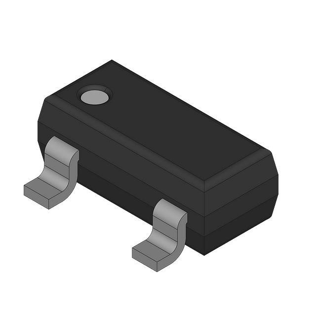
Figure 2. MMBT4401 Device Package
Ordering Information
Part Number
Marking
Package
Packing Method
2N4401BU
2N4401
TO-92 3L
Bulk
2N4401TF
2N4401
TO-92 3L
Tape and Reel
2N4401TFR
2N4401
TO-92 3L
Tape and Reel
2N4401TA
2N4401
TO-92 3L
Ammo
2N4401TAR
2N4401
TO-92 3L
Ammo
MMBT4401
2X
SOT-23 3L
Tape and Reel
© 2001 Semiconductor Components Industries, LLC.
September-2017, Rev. 2
Publication Order Number:
MMBT4401/D
�Stresses exceeding the absolute maximum ratings may damage the device. The device may not function or be operable above the recommended operating conditions and stressing the parts to these levels is not recommended. In addition, extended exposure to stresses above the recommended operating conditions may affect device reliability. The
absolute maximum ratings are stress ratings only. Values are at TA = 25°C unless otherwise noted.
Symbol
Parameter
Value
Unit
VCEO
Collector-Emitter Voltage
40
V
VCBO
Collector-Base Voltage
60
V
VEBO
Emitter-Base Voltage
6.0
V
600
mA
-55 to +150
°C
IC
TJ, TSTG
Collector Current - Continuous
Operating and Storage Junction Temperature Range
Notes:
1. These ratings are based on a maximum junction temperature of 150°C.
2. These are steady-state limits. ON Semiconductor should be consulted on applications involving pulsed or lowduty cycle operations.
Thermal Characteristics
Values are at TA = 25°C unless otherwise noted.
Symbol
PD
Max.
Parameter
Total Device Dissipation
Unit
2N4401(3)
MMBT4401(4)
625
350
mW
2.8
mW/°C
Derate Above 25°C
5.0
RθJC
Thermal Resistance, Junction to Case
83.3
RθJA
Thermal Resistance, Junction to Ambient
200
°C/W
357
°C/W
Notes:
3. PCB size: FR-4, 76 mm x 114 mm x 1.57 mm (3.0 inch x 4.5 inch x 0.062 inch) with minimum land pattern size.
4. Device mounted on FR-4 PCB 1.6 inch x 1.6 inch x 0.06 inch.
www.onsemi.com
2
2N4401 / MMBT4401 — NPN General-Purpose Amplifier
Absolute Maximum Ratings(1),(2)
�Values are at TA = 25°C unless otherwise noted.
Symbol
Parameter
Conditions
Min.
Max.
Unit
V(BR)CEO
Collector-Emitter Breakdown
Voltage(5)
IC = 1.0 mA, IB = 0
40
V
V(BR)CBO
Collector-Base Breakdown
Voltage
IC = 0.1 mA, IE = 0
60
V
V(BR)EBO
Emitter-Base Breakdown Voltage
IE = 0.1 mA, IC = 0
6.0
V
Base Cut-Off Current
VCE = 35 V, VEB = 0.4 V
Collector Cut-Off Current
VCE = 35 V, VEB = 0.4 V
IBL
ICEX
hFE
(5)
DC Current Gain
IC = 0.1 mA, VCE = 1.0 V
20
IC = 1.0 mA, VCE = 1.0 V
40
IC = 10 mA, VCE = 1.0 V
80
IC = 150 mA, VCE = 1.0 V
100
IC = 500 mA, VCE = 2.0 V
40
0.1
μA
0.1
μA
300
IC = 150 mA, IB = 15 mA
0.40
IC = 500 mA, IB = 50 mA
0.75
VCE(sat)
Collector-Emitter Saturation
Voltage(5)
VBE(sat)
Base-Emitter Saturation Voltage(5)
fT
Current Gain - Bandwidth Product
IC = 20 mA, VCE = 10 V,
f = 100 MHz
Ccb
Collector-Base Capacitance
VCB = 5.0 V, IE = 0,
f = 140 kHz
6.5
pF
Ceb
Emitter-Base Capacitance
VBE = 0.5 V, IC = 0,
f = 140 kHz
30
pF
hie
Input Impedance
IC = 1.0 mA, VCE = 10 V,
f = 1.0 kHz
1.0
15.0
kΩ
hre
Voltage Feedback Ratio
IC = 1.0 mA, VCE = 10 V,
f = 1.0 kHz
0.1
8.0
x10-4
hfe
Small-Signal Current Gain
IC = 1.0 mA, VCE = 10 V,
f = 1.0 kHz
40
500
hoe
Output Admittance
IC = 1.0 mA, VCE = 10 V,
f = 1.0 kHz
1.0
30
μmhos
15
ns
td
Delay Time
tr
Rise Time
ts
Storage Time
tf
Fall Time
IC = 150 mA, IB = 15 mA
0.75
IC = 500 mA, IB = 50 mA
VCC = 30 V, VEB = 2 V,
IC = 150 mA, IB1 = 15 mA
VCC = 30 V, IC = 150 mA,
IB1 = IB2 = 15 mA
Note:
5. Pulse test: pulse width ≤ 300 μs, duty cycle ≤ 2.0%.
www.onsemi.com
3
0.95
1.20
250
V
V
MHz
20
ns
225
ns
30
ns
2N4401 / MMBT4401 — NPN General-Purpose Amplifier
Electrical Characteristics
�400
125 °C
300
200
25 °C
100
- 40 °C
0
0.1
0.3
1
3
10
30
100
I C - COLLECTOR CURRENT (mA)
300
V BESAT - BASE-EMITTER VOLTAGE (V)
β = 10
- 40 °C
0.8
25 °C
125 °C
0.6
0.4
1
I
C
10
100
- COLLECTOR CURRENT (mA)
0.4
β = 10
0.3
25 °C
0.1
- 40 °C
1
10
100
I C - COLLECTOR CURRENT (mA)
500
500
1
VCE = 5V
0.8
- 40 °C
25 °C
0.6
125 °C
0.4
0.2
0.1
1
10
I C - COLLECTOR CURRENT (mA)
25
Figure 6. Base-Emitter On Voltage vs.
Collector Current
Figure 5. Base-Emitter Saturation Voltage
vs. Collector Current
500
100
V
CB
20
= 40V
CAPACITANCE (pF)
I CBO - COLLECTOR CURRENT (nA)
125 °C
0.2
Figure 4. Collector-Emitter Saturation Voltage vs.
Collector Current
Figure 3. Typical Pulsed Current Gain vs.
Collector Current
1
V CESAT - COLLECTOR-EMITTER VOLTAGE (V)
V CE = 5V
V BE(ON) - BASE-EMITTER ON VOLTAGE (V)
h FE - TYPICAL PULSED CURRENT GAIN
500
10
1
0.1
16
12
C
te
8
4
25
50
75
100
125
T A - AMBIENT TEMPERATURE (° C)
Figure 7. Collector Cut-Off Current vs.
Ambient Temperature
150
f = 1 MHz
0.1
C ob
1
10
REVERSE BIAS VOLTAGE (V)
100
Figure 8. Emitter Transition and Output Capacitance
vs. Reverse Bias Voltage
www.onsemi.com
4
2N4401 / MMBT4401 — NPN General-Purpose Amplifier
Typical Performance Characteristics
�400
I B1 = I B2 =
320
400
Ic
TIME (nS)
TIME (nS)
V cc = 25 V
240
160
240
tr
td
0.5
SOT-23
0.25
125
150
CHAR. RELATIVE TO VALUES AT TA = 25oC
Figure 11. Power Dissipation vs.
Ambient Temperature
2.4
V CE = 10 V
I C = 10 mA
2
h re
h ie
h fe
1.2
hoe
0.8
0.4
0
20
40
60
80
T A - AMBIENT TEMPERATURE ( o C)
1000
V CE = 10 V
T A = 25oC
6
hoe
4
h re
2
h fe
0
h ie
0
10
20
30
40
50
I C - COLLECTOR CURRENT (mA)
60
Figure 12. Common Emitter Characteristics
1.6
0
8
100
Figure 13. Common Emitter Characteristics
CHAR. RELATIVE TO VALUES AT VCE = 10V
PD - POWER DISSIPATION (W)
SOT-223
TO-92
50
75
100
o
TEMPERATURE ( C)
100
I C - COLLECTOR CURRENT (mA)
Figure 10. Switching Times vs.Collector Current
1
25
0
10
1000
CHAR. RELATIVE TO VALUES AT I C= 10mA
100
I C - COLLECTOR CURRENT (mA)
Figure 9. Turn-On and Turn-Off Times vs.
Collector Current
0
tf
80
t on
0
ts
160
t off
80
0.75
10
320
V cc = 25 V
0
10
Ic
I B1 = I B2 =
10
1.3
I C = 10 mA
T A = 25oC
1.25
1.2
h fe
1.15
h ie
1.1
1.05
1
h re
0.95
0.9
0.85
hoe
0.8
0.75
0
5
10
15
20
25
30
VCE - COLLECTOR VOLTAGE (V)
Figure 14. Common Emitter Characteristics
www.onsemi.com
5
35
2N4401 / MMBT4401 — NPN General-Purpose Amplifier
Typical Performance Characteristics (Continued)
�2N4401 / MMBT4401 — NPN General-Purpose Amplifier
Physical Dimensions
D
Figure 15. 3-Lead, TO-92, JEDEC TO-92 Compliant Straight Lead Configuration, Bulk Type
www.onsemi.com
6
�2N4401 / MMBT4401 — NPN General-Purpose Amplifier
Physical Dimensions (Continued)
Figure 16. 3-Lead, TO-92, Molded, 0.2 In Line Spacing Lead Form, Ammo, Tape and Reel Type
www.onsemi.com
7
�0.95
2.92±0.20
3
1.40
1.30+0.20
-0.15
1
2.20
2
0.60
0.37
(0.29)
0.95
0.20
1.00
A B
1.90
1.90
LAND PATTERN
RECOMMENDATION
SEE DETAIL A
1.20 MAX
0.10
0.00
(0.93)
0.10
C
C
2.40±0.30
NOTES: UNLESS OTHERWISE SPECIFIED
GAGE PLANE
0.23
0.08
0.25
0.20 MIN
(0.55)
SEATING
PLANE
A) REFERENCE JEDEC REGISTRATION
TO-236, VARIATION AB, ISSUE H.
B) ALL DIMENSIONS ARE IN MILLIMETERS.
C) DIMENSIONS ARE INCLUSIVE OF BURRS,
MOLD FLASH AND TIE BAR EXTRUSIONS.
D) DIMENSIONING AND TOLERANCING PER
ASME Y14.5M - 1994.
E) DRAWING FILE NAME: MA03DREV10
SCALE: 2X
Figure 17. 3-LEAD, SOT23, JEDEC TO-236, LOW PROFILE
www.onsemi.com
8
2N4401 / MMBT4401 — NPN General-Purpose Amplifier
Physical Dimensions (Continued)
�ON Semiconductor and
are trademarks of Semiconductor Components Industries, LLC dba ON Semiconductor or its subsidiaries in the United States and/or other countries.
ON Semiconductor owns the rights to a number of patents, trademarks, copyrights, trade secrets, and other intellectual property. A listing of ON Semiconductor’s product/patent
coverage may be accessed at www.onsemi.com/site/pdf/Patent−Marking.pdf. ON Semiconductor reserves the right to make changes without further notice to any products herein.
ON Semiconductor makes no warranty, representation or guarantee regarding the suitability of its products for any particular purpose, nor does ON Semiconductor assume any liability
arising out of the application or use of any product or circuit, and specifically disclaims any and all liability, including without limitation special, consequential or incidental damages.
Buyer is responsible for its products and applications using ON Semiconductor products, including compliance with all laws, regulations and safety requirements or standards,
regardless of any support or applications information provided by ON Semiconductor. “Typical” parameters which may be provided in ON Semiconductor data sheets and/or
specifications can and do vary in different applications and actual performance may vary over time. All operating parameters, including “Typicals” must be validated for each customer
application by customer’s technical experts. ON Semiconductor does not convey any license under its patent rights nor the rights of others. ON Semiconductor products are not
designed, intended, or authorized for use as a critical component in life support systems or any FDA Class 3 medical devices or medical devices with a same or similar classification
in a foreign jurisdiction or any devices intended for implantation in the human body. Should Buyer purchase or use ON Semiconductor products for any such unintended or unauthorized
application, Buyer shall indemnify and hold ON Semiconductor and its officers, employees, subsidiaries, affiliates, and distributors harmless against all claims, costs, damages, and
expenses, and reasonable attorney fees arising out of, directly or indirectly, any claim of personal injury or death associated with such unintended or unauthorized use, even if such
claim alleges that ON Semiconductor was negligent regarding the design or manufacture of the part. ON Semiconductor is an Equal Opportunity/Affirmative Action Employer. This
literature is subject to all applicable copyright laws and is not for resale in any manner.
PUBLICATION ORDERING INFORMATION
LITERATURE FULFILLMENT:
Literature Distribution Center for ON Semiconductor
19521 E. 32nd Pkwy, Aurora, Colorado 80011 USA
Phone: 303−675−2175 or 800−344−3860 Toll Free USA/Canada
Fax: 303−675−2176 or 800−344−3867 Toll Free USA/Canada
Email: orderlit@onsemi.com
❖
© Semiconductor Components Industries, LLC
N. American Technical Support: 800−282−9855 Toll Free
USA/Canada
Europe, Middle East and Africa Technical Support:
Phone: 421 33 790 2910
Japan Customer Focus Center
Phone: 81−3−5817−1050
ON Semiconductor Website: www.onsemi.com
Order Literature: http://www.onsemi.com/orderlit
For additional information, please contact your local
Sales Representative
www.onsemi.com
�