MMDL301T1G
Silicon Hot-Carrier Diodes
Schottky Barrier Diode
These devices are designed primarily for high−efficiency UHF and
VHF detector applications. They are readily adaptable to many other
fast switching RF and digital applications. They are supplied in an
inexpensive plastic package for low−cost, high−volume consumer
and industrial/commercial requirements. They are available in a
Surface Mount package.
Features
•
•
•
•
Extremely Low Minority Carrier Lifetime − 15 ps (Typ)
Very Low Capacitance − 1.5 pF (Max) @ VR = 15 V
Low Reverse Leakage − IR = 13 nAdc (Typ)
These Devices are Pb−Free, Halogen Free/BFR Free and are RoHS
Compliant
http://onsemi.com
30 VOLTS SILICON
HOT−CARRIER DETECTOR
AND SWITCHING DIODES
1
CATHODE
2
ANODE
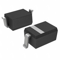
PLASTIC
SOD−323
CASE 477
STYLE 1
2
MAXIMUM RATINGS (TJ = 125°C unless otherwise noted)
Rating
Symbol
Value
Unit
VR
30
V
Symbol
Max
Unit
200
1.57
mW
mW/°C
Reverse Voltage
1
THERMAL CHARACTERISTICS
Characteristic
Total Device Dissipation FR−5 Board,
(Note 1) @TA = 25°C
Derate above 25°C
PD
Thermal Resistance, Junction−to−Ambient
RqJA
635
°C/W
Junction and Storage Temperature Range
TJ, Tstg
−55 to +150
°C
MARKING DIAGRAM
4T M G
G
Stresses exceeding Maximum Ratings may damage the device. Maximum
Ratings are stress ratings only. Functional operation above the Recommended
Operating Conditions is not implied. Extended exposure to stresses above the
Recommended Operating Conditions may affect device reliability.
1. FR−5 Minimum Pad
ELECTRICAL CHARACTERISTICS (TA = 25°C unless otherwise noted)
Characteristic
Symbol
Min
Typ
Max
Unit
V(BR)R
30
−
−
V
Total Capacitance
(VR = 15 V, f = 1.0 MHz) Figure 1
CT
−
0.9
1.5
pF
Reverse Leakage
(VR = 25 V) Figure 3
IR
−
13
200
nAdc
Forward Voltage
(IF = 1.0 mAdc) Figure 4
VF
−
0.38
0.45
Vdc
Forward Voltage
(IF = 10 mAdc) Figure 4
VF
−
0.52
0.6
Vdc
Reverse Breakdown Voltage
(IR = 10 mA)
© Semiconductor Components Industries, LLC, 2010
September, 2010− Rev. 2
1
4T
M
G
= Device Code
= Date Code*
= Pb−Free Package
(Note: Microdot may be in either location)
*Date Code orientation may vary depending
upon manufacturing location.
ORDERING INFORMATION
Device
Package
Shipping†
MMDL301T1G
SOD−323
(Pb−Free)
3000 / Tape & Reel
†For information on tape and reel specifications,
including part orientation and tape sizes, please
refer to our Tape and Reel Packaging Specifications
Brochure, BRD8011/D.
Publication Order Number:
MMDL301T1/D
�MMDL301T1G
TYPICAL ELECTRICAL CHARACTERISTICS
500
2.8
t , MINORITY CARRIER LIFETIME (ps)
C T, TOTAL CAPACITANCE (pF)
f = 1.0 MHz
2.4
2.0
1.6
1.2
0.8
0.4
400
KRAKAUER METHOD
300
200
100
0
0
0
3.0
6.0
9.0
12
15
18
21
VR, REVERSE VOLTAGE (VOLTS)
24
27
30
0
Figure 1. Total Capacitance
30
40
50
60
70
IF, FORWARD CURRENT (mA)
80
90
100
100
IF, FORWARD CURRENT (mA)
IR, REVERSE LEAKAGE (m A)
20
Figure 2. Minority Carrier Lifetime
10
TA = 100°C
1.0
75°C
0.1
25°C
0.01
0.001
10
10
TA = -�40°C
TA = 85°C
1.0
TA = 25°C
0.1
0
6.0
12
18
VR, REVERSE VOLTAGE (VOLTS)
24
30
0.2
Figure 3. Reverse Leakage
IF(PEAK)
0.4
0.6
0.8
VF, FORWARD VOLTAGE (VOLTS)
1.0
Figure 4. Forward Voltage
CAPACITIVE
CONDUCTION
IR(PEAK)
FORWARD
CONDUCTION
SINUSOIDAL
GENERATOR
BALLAST
NETWORK
(PADS)
STORAGE
CONDUCTION
PADS
DUT
Figure 5. Krakauer Method of Measuring Lifetime
http://onsemi.com
2
SAMPLING
OSCILLOSCOPE
(50 W INPUT)
1.2
�MECHANICAL CASE OUTLINE
PACKAGE DIMENSIONS
2
1
STYLE 1
SOD−323
CASE 477−02
ISSUE H
2
SCALE 4:1
NOTES:
1. DIMENSIONING AND TOLERANCING PER ANSI
Y14.5M, 1982.
2. CONTROLLING DIMENSION: MILLIMETERS.
3. LEAD THICKNESS SPECIFIED PER L/F DRAWING
WITH SOLDER PLATING.
4. DIMENSIONS A AND B DO NOT INCLUDE MOLD
FLASH, PROTRUSIONS OR GATE BURRS.
5. DIMENSION L IS MEASURED FROM END OF RADIUS.
HE
D
b
1
2
E
A3
A
C
NOTE 3
DATE 13 MAR 2007
1
STYLE 2
L
A1
NOTE 5
MILLIMETERS
DIM MIN
NOM MAX
A
0.80
0.90
1.00
A1 0.00
0.05
0.10
A3
0.15 REF
b
0.25
0.32
0.4
C 0.089
0.12 0.177
D
1.60
1.70
1.80
E
1.15
1.25
1.35
L
0.08
HE
2.30
2.50
2.70
INCHES
NOM MAX
0.035 0.040
0.002 0.004
0.006 REF
0.010 0.012 0.016
0.003 0.005 0.007
0.062 0.066 0.070
0.045 0.049 0.053
0.003
0.090 0.098 0.105
MIN
0.031
0.000
GENERIC
MARKING DIAGRAM*
SOLDERING FOOTPRINT*
XX M
0.63
0.025
STYLE 1
0.83
0.033
*This information is generic. Please refer to
device data sheet for actual part marking.
Pb−Free indicator, “G” or microdot “ G”,
may or may not be present.
2.85
0.112
*For additional information on our Pb−Free strategy and soldering
details, please download the ON Semiconductor Soldering and
Mounting Techniques Reference Manual, SOLDERRM/D.
DESCRIPTION:
98ASB17533C
SOD−323
STYLE 2
XX = Specific Device Code
M = Date Code
1.60
0.063
DOCUMENT NUMBER:
XX M
STYLE 1:
PIN 1. CATHODE (POLARITY BAND)
2. ANODE
STYLE 2:
NO POLARITY
Electronic versions are uncontrolled except when accessed directly from the Document Repository.
Printed versions are uncontrolled except when stamped “CONTROLLED COPY” in red.
PAGE 1 OF 1
ON Semiconductor and
are trademarks of Semiconductor Components Industries, LLC dba ON Semiconductor or its subsidiaries in the United States and/or other countries.
ON Semiconductor reserves the right to make changes without further notice to any products herein. ON Semiconductor makes no warranty, representation or guarantee regarding
the suitability of its products for any particular purpose, nor does ON Semiconductor assume any liability arising out of the application or use of any product or circuit, and specifically
disclaims any and all liability, including without limitation special, consequential or incidental damages. ON Semiconductor does not convey any license under its patent rights nor the
rights of others.
© Semiconductor Components Industries, LLC, 2019
www.onsemi.com
�onsemi,
, and other names, marks, and brands are registered and/or common law trademarks of Semiconductor Components Industries, LLC dba “onsemi” or its affiliates
and/or subsidiaries in the United States and/or other countries. onsemi owns the rights to a number of patents, trademarks, copyrights, trade secrets, and other intellectual property.
A listing of onsemi’s product/patent coverage may be accessed at www.onsemi.com/site/pdf/Patent−Marking.pdf. onsemi reserves the right to make changes at any time to any
products or information herein, without notice. The information herein is provided “as−is” and onsemi makes no warranty, representation or guarantee regarding the accuracy of the
information, product features, availability, functionality, or suitability of its products for any particular purpose, nor does onsemi assume any liability arising out of the application or use
of any product or circuit, and specifically disclaims any and all liability, including without limitation special, consequential or incidental damages. Buyer is responsible for its products
and applications using onsemi products, including compliance with all laws, regulations and safety requirements or standards, regardless of any support or applications information
provided by onsemi. “Typical” parameters which may be provided in onsemi data sheets and/or specifications can and do vary in different applications and actual performance may
vary over time. All operating parameters, including “Typicals” must be validated for each customer application by customer’s technical experts. onsemi does not convey any license
under any of its intellectual property rights nor the rights of others. onsemi products are not designed, intended, or authorized for use as a critical component in life support systems
or any FDA Class 3 medical devices or medical devices with a same or similar classification in a foreign jurisdiction or any devices intended for implantation in the human body. Should
Buyer purchase or use onsemi products for any such unintended or unauthorized application, Buyer shall indemnify and hold onsemi and its officers, employees, subsidiaries, affiliates,
and distributors harmless against all claims, costs, damages, and expenses, and reasonable attorney fees arising out of, directly or indirectly, any claim of personal injury or death
associated with such unintended or unauthorized use, even if such claim alleges that onsemi was negligent regarding the design or manufacture of the part. onsemi is an Equal
Opportunity/Affirmative Action Employer. This literature is subject to all applicable copyright laws and is not for resale in any manner.
PUBLICATION ORDERING INFORMATION
LITERATURE FULFILLMENT:
Email Requests to: orderlit@onsemi.com
onsemi Website: www.onsemi.com
◊
TECHNICAL SUPPORT
North American Technical Support:
Voice Mail: 1 800−282−9855 Toll Free USA/Canada
Phone: 011 421 33 790 2910
Europe, Middle East and Africa Technical Support:
Phone: 00421 33 790 2910
For additional information, please contact your local Sales Representative
�