MPS6521 (NPN) MPS6523 (PNP)
MPS6521 is a Preferred Device
Amplifier Transistors
Features
• Voltage and Current are Negative for PNP Transistors • Pb−Free Packages are Available*
MAXIMUM RATINGS
Rating Collector −Emitter Voltage MPS6521 MPS6523 Collector −Base Voltage MPS6521 MPS6523 Emitter −Base Voltage Collector Current − Continuous Total Device Dissipation @ TA = 25°C Derate above 25°C Total Device Dissipation @ TC = 25°C Derate above 25°C Operating and Storage Junction Temperature Range VEBO IC PD PD TJ, Tstg VCBO 40 − 4.0 100 625 5.0 1.5 12 −55 to +150 − 25 Vdc mAdc mW mW/°C W mW/°C °C
1 2 3
http://onsemi.com
COLLECTOR 3 COLLECTOR 3 2 BASE 1 EMITTER 1 EMITTER
Symbol VCEO
NPN 25 −
PNP − 25
Unit Vdc 2 BASE
Vdc
MARKING DIAGRAM
TO−92 CASE 29−11 STYLE 1
MPS 652x AYWW G G
THERMAL CHARACTERISTICS
Characteristic Thermal Resistance, Junction−to−Ambient (Printed Circuit Board Mounting) Thermal Resistance, Junction−to−Case Symbol RqJA RqJC Max 200 83.3 Unit °C/W °C/W
Stresses exceeding Maximum Ratings may damage the device. Maximum Ratings are stress ratings only. Functional operation above the Recommended Operating Conditions is not implied. Extended exposure to stresses above the Recommended Operating Conditions may affect device reliability.
MPS652x = Device Code x = 1 or 3 A = Assembly Location Y = Year WW = Work Week G = Pb−Free Package (Note: Microdot may be in either location)
ORDERING INFORMATION
Device MPS6521 MPS6521G MPS6521RLRA MPS6521RLRAG MPS6523 MPS6523G Package TO−92 TO−92 (Pb−Free) TO−92 TO−92 (Pb−Free) TO−92 TO−92 (Pb−Free) Shipping † 5000 Units/Box 5000 Units/Box 2000/Tape & Reel 2000/Tape & Reel 5000 Units/Box 5000 Units/Box
*For additional information on our Pb−Free strategy and soldering details, please download the ON Semiconductor Soldering and Mounting Techniques Reference Manual, SOLDERRM/D.
†For information on tape and reel specifications, including part orientation and tape sizes, please refer to our Tape and Reel Packaging Specifications Brochure, BRD8011/D.
Preferred devices are recommended choices for future use and best overall value.
© Semiconductor Components Industries, LLC, 2006
1
March, 2006 − Rev. 3
Publication Order Number: MPS6521/D
�MPS6521 (NPN)
MPS6523 (PNP)
ELECTRICAL CHARACTERISTICS (TA = 25°C unless otherwise noted)
Characteristic OFF CHARACTERISTICS Collector −Emitter Breakdown Voltage (IC = 0.5 mAdc, IB = 0) Emitter −Base Breakdown Voltage (IE = 10 mAdc, IC = 0) Collector Cutoff Current (VCB = 30 Vdc, IE = 0) (VCB = 20 Vdc, IE = 0) ON CHARACTERISTICS DC Current Gain (IC = 100 mAdc, VCE = 10 Vdc) (IC = 2.0 mAdc, VCE = 10 Vdc) (IC = 100 mAdc, VCE = 10 Vdc) (IC = 2.0 mAdc, VCE = 10 Vdc) Collector −Emitter Saturation Voltage (IC = 50 mAdc, IB = 5.0 mAdc) SMALL− SIGNAL CHARACTERISTICS Output Capacitance (VCB = 10 Vdc, IE = 0, f = 1.0 MHz) Noise Figure (IC = 10 mAdc, VCE = 5.0 Vdc, RS = 10 k W, Power Bandwidth = 15.7 kHz, 3.0 dB points @ 10 Hz and 10 kHz) Cobo NF − − 3.5 3.0 pF dB hFE MPS6521 MPS6521 MPS6523 MPS6523 VCE(sat) 150 300 150 300 − − 600 − 600 0.5 Vdc − MPS6521 MPS6523 V(BR)CEO V(BR)EBO ICBO − − 0.05 0.05 25 4.0 − − Vdc Vdc mAdc Symbol Min Max Unit
NPN MPS6521 EQUIVALENT SWITCHING TIME TEST CIRCUITS
+3.0 V 300 ns DUTY CYCLE = 2% −0.5 V
很抱歉,暂时无法提供与“MPS6521RLRA”相匹配的价格&库存,您可以联系我们找货
免费人工找货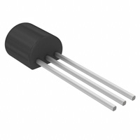


 工商网监
湘ICP备2023018690号
工商网监
湘ICP备2023018690号
