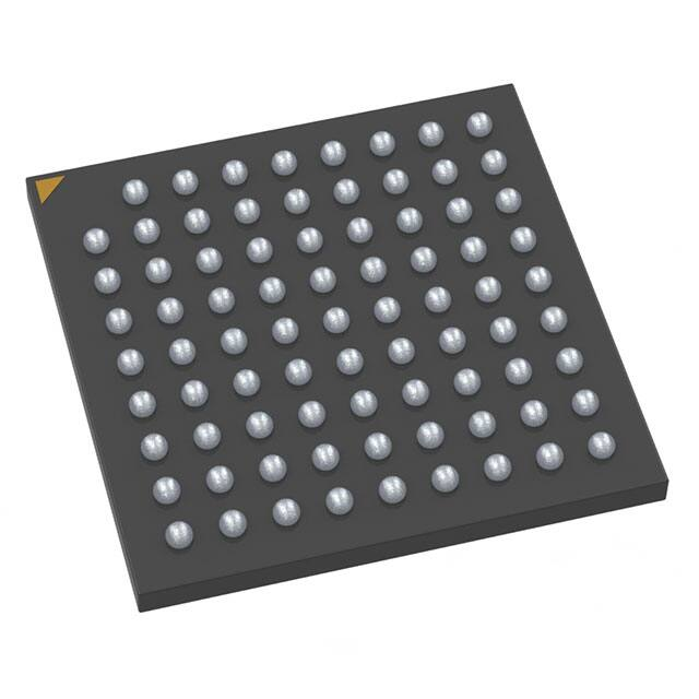
MT9V128
MT9V128 1/4-Inch Color
CMOS NTSC/PAL Digital
Image SOC with Distortion
Correction and Overlay
Processor
www.onsemi.com
Table 1. KEY PARAMETERS
Parameter
Typical Value
Pixel Size and Type
5.6 μm × 5.6 μm Active Pinnedphotodiode with
High−sensitivity Mode for Low−light Conditions
Sensor Format
680 (H) × 512 (V) (includes ±2.5% of Rows and
Columns for Lens Alignment)
NTSC Output
720 H × 480 V
PAL Output
720 H × 576 V
ORDERING INFORMATION
See detailed ordering and shipping information on page 4 of
this data sheet.
Imaging Area
Total Array Size:
3.584 mm x 2.688 mm
Optical Format
1/ −inch
4
Frame Rate
50/60 Fields/sec
Sensor Scan Mode
Progressive Scan
Color Filter Array
RGB Standard Bayer
Shutter Type
Electronic Rolling Shutter (ERS)
Automatic Functions
Exposure, White Balance, Black Level Offset
Correction, Flicker Avoidance, Color Saturation
Control, On−the−fly Defect Correction, Aperture
Correction
Programmable Controls
Exposure, White Balance, Horizontal and
Vertical Blanking, Color, Sharpness, Gamma
Correction, Lens Shading Correction, Horizontal
and Vertical Image Flip, Zoom, Windowing,
Sampling Rates, GPIO Control
Lens Distortion
Correction (Note 1)
IBGA63 9x9
CASE 503AL
Features (continued)
• Integrated Microcontroller for Flexibility
• On−chip Image Flow Processor Performs
Maximum Lens Distortion Supported Up to 25%
Flexible Algorithm that can be Calibrated for
many Wide−angle Lenses through Software
Tools Perspective Correction
•
•
•
•
•
• Low−power CMOS Image Sensor with Integrated Image Flow
•
•
•
• 1/4−inch Optical Format, VGA Resolution (640 (H) × 480 (V))
• ±2.5% Additional Columns and Rows to Compensate for Lens
•
•
Features
Processor (IFP) and Video Encoder
Alignment Tolerances
• Integrated Lens Distortion Correction
• Overlay Generator for Dynamic Bitmap Overlay
• Integrated Video Encoder for NTSC/PAL with Overlay Capability
and 10−bit I−DAC
© Semiconductor Components Industries, LLC, 2010
January, 2019 − Rev. 7
1
Sophisticated Processing, Such as Color
Recovery and Correction, Sharpening,
Gamma, Lens Shading Correction,
On−the−fly Defect Correction, Auto White
Balancing, and Auto Exposure
Auto Black Level Calibration
10−bit, On−chip Analog−to−digital
Converter (ADC)
Internal Master Clock Generated by
On−chip Phaselocked Loop (PLL)
Two−wire Serial Programming Interface
Interface to Low−cost Flash through SPI
Bus
High−level Host Command Interface
Stand Alone Operation Support
Comprehensive Tool Support for Overlay
Generation and Lens Correction Setup
Development System with DevWare
Overlay Generation and Compilation Tools
Applications
• Automotive Rearview Camera and Side
Mirror
• Blind Spot and Surround View
Publication Order Number:
MT9V128/D
�MT9V128
TABLE OF CONTENTS
Features . . . . . . . . . . . . . . . . . . . . . . . . . . . . . . . . . . . . . . . . . . . . . . . . . . . . . . . . . . . . . . . . . . . . . . . . . . . . . . . . . . . . . . . . . . . . . . . . 1
Applications . . . . . . . . . . . . . . . . . . . . . . . . . . . . . . . . . . . . . . . . . . . . . . . . . . . . . . . . . . . . . . . . . . . . . . . . . . . . . . . . . . . . . . . . . . . . . 1
Ordering Information . . . . . . . . . . . . . . . . . . . . . . . . . . . . . . . . . . . . . . . . . . . . . . . . . . . . . . . . . . . . . . . . . . . . . . . . . . . . . . . . . . . . . 4
New Features . . . . . . . . . . . . . . . . . . . . . . . . . . . . . . . . . . . . . . . . . . . . . . . . . . . . . . . . . . . . . . . . . . . . . . . . . . . . . . . . . . . . . . . . . . . 4
General Description . . . . . . . . . . . . . . . . . . . . . . . . . . . . . . . . . . . . . . . . . . . . . . . . . . . . . . . . . . . . . . . . . . . . . . . . . . . . . . . . . . . . . . 5
Architecture . . . . . . . . . . . . . . . . . . . . . . . . . . . . . . . . . . . . . . . . . . . . . . . . . . . . . . . . . . . . . . . . . . . . . . . . . . . . . . . . . . . . . . . . . . . . . 5
System Block Diagram . . . . . . . . . . . . . . . . . . . . . . . . . . . . . . . . . . . . . . . . . . . . . . . . . . . . . . . . . . . . . . . . . . . . . . . . . . . . . . . . . . . 6
Pin Descriptions and Assignments . . . . . . . . . . . . . . . . . . . . . . . . . . . . . . . . . . . . . . . . . . . . . . . . . . . . . . . . . . . . . . . . . . . . . . . . . 7
SOC Description . . . . . . . . . . . . . . . . . . . . . . . . . . . . . . . . . . . . . . . . . . . . . . . . . . . . . . . . . . . . . . . . . . . . . . . . . . . . . . . . . . . . . . . . 11
Sensor Pixel Array . . . . . . . . . . . . . . . . . . . . . . . . . . . . . . . . . . . . . . . . . . . . . . . . . . . . . . . . . . . . . . . . . . . . . . . . . . . . . . . . . . . . . . 13
Usage Modes . . . . . . . . . . . . . . . . . . . . . . . . . . . . . . . . . . . . . . . . . . . . . . . . . . . . . . . . . . . . . . . . . . . . . . . . . . . . . . . . . . . . . . . . . . 21
External Overlay . . . . . . . . . . . . . . . . . . . . . . . . . . . . . . . . . . . . . . . . . . . . . . . . . . . . . . . . . . . . . . . . . . . . . . . . . . . . . . . . . . . . . . . . 23
Multicamera Support . . . . . . . . . . . . . . . . . . . . . . . . . . . . . . . . . . . . . . . . . . . . . . . . . . . . . . . . . . . . . . . . . . . . . . . . . . . . . . . . . . . . 23
External Signal Processing . . . . . . . . . . . . . . . . . . . . . . . . . . . . . . . . . . . . . . . . . . . . . . . . . . . . . . . . . . . . . . . . . . . . . . . . . . . . . . . 24
Slave Two−Wire Serial Interface . . . . . . . . . . . . . . . . . . . . . . . . . . . . . . . . . . . . . . . . . . . . . . . . . . . . . . . . . . . . . . . . . . . . . . . . . . 31
Integrated Lens Distortion Correction . . . . . . . . . . . . . . . . . . . . . . . . . . . . . . . . . . . . . . . . . . . . . . . . . . . . . . . . . . . . . . . . . . . . . . 34
Overlay Capability . . . . . . . . . . . . . . . . . . . . . . . . . . . . . . . . . . . . . . . . . . . . . . . . . . . . . . . . . . . . . . . . . . . . . . . . . . . . . . . . . . . . . . 37
Serial Memory Partition . . . . . . . . . . . . . . . . . . . . . . . . . . . . . . . . . . . . . . . . . . . . . . . . . . . . . . . . . . . . . . . . . . . . . . . . . . . . . . . . . . 38
Overlay Adjustment . . . . . . . . . . . . . . . . . . . . . . . . . . . . . . . . . . . . . . . . . . . . . . . . . . . . . . . . . . . . . . . . . . . . . . . . . . . . . . . . . . . . . 39
Overlay Character Generator . . . . . . . . . . . . . . . . . . . . . . . . . . . . . . . . . . . . . . . . . . . . . . . . . . . . . . . . . . . . . . . . . . . . . . . . . . . . . 40
Modes and Timing . . . . . . . . . . . . . . . . . . . . . . . . . . . . . . . . . . . . . . . . . . . . . . . . . . . . . . . . . . . . . . . . . . . . . . . . . . . . . . . . . . . . . . 43
Electrical Specifications . . . . . . . . . . . . . . . . . . . . . . . . . . . . . . . . . . . . . . . . . . . . . . . . . . . . . . . . . . . . . . . . . . . . . . . . . . . . . . . . . . 54
Spectral Characteristics . . . . . . . . . . . . . . . . . . . . . . . . . . . . . . . . . . . . . . . . . . . . . . . . . . . . . . . . . . . . . . . . . . . . . . . . . . . . . . . . . 62
www.onsemi.com
2
�MT9V128
Table 2. KEY PARAMETERS (continued)
Parameter
Overlay Support (Note 1)
Typical Value
Utilizes SPI interface to load overlay data from external flash/EEPROM
memory with the following features:
− Overlay Size 360 x 480 pixel rendered into 720 x 480 pixel display format
− Up to four (4) overlays may be blended simultaneously
− Selectable readout: Rotating order user selected
− Dynamic scenes by loading pre−rendered frames from external memory
− Palette of 32 colors out of 64,000
− 8 colors per bitmap
− Blend factor dynamically programmable for smooth transitions
− Fast Update rate of up to 30 fps
− Every bitmap object has independent x/y position
− Statistic Engine to calibrate optical alignment
− Number Generator
External Overlay Processing Support
Digital input to on−chip NTSC encoder allows for external overlay,
processing by a DSP, or FPGA
Windowing
Programmable to any size
Max Analog Gain
0.5–16x
ADC
10−bit, on−chip
Output Interface
Analog composite video out, single−ended or differential; 8−, 10−bit parallel
digital output
Output Data Formats (Note 1)
Digital: Raw Bayer 8−,10−bit, CCIR656, 565RGB, 555RGB, 444RGB
Data Rate
Parallel: 27 MB/s
NTSC: 60 fields/sec
PAL: 50 fields/sec
Control Interface
Two−wire I/F for register interface plus high−level command exchange. SPI
port to interface to external memory to load overlay data, register settings,
or firmware extensions.
Input Clock for PLL
27 MHz
SPI Clock Frequencies
4.5 − 9.0 − 18 MHz, programmable
Supply Voltage
Analog: 2.8 V ±5%
Core: 1.8 V ±5%
IO: 2.8 V ±5%
Power Consumption
Full resolution at 60 fps: Flash Configuration
Mode
• A valid Flash device identifier is detected BUT the
Flash device DOES NOT contain valid configuration
records, then
♦ Enter Auto Configuration
The device supports an auto−configuration feature.
During system start−up, the device first detects whether an
SPI Flash device is attached to the MT9V128. If not, it will
then sample the state of a number of GPI inputs including
FRAME_VALID, LINE_VALID and DOUT_LSB0. For
more information, see Table 16, “GPIO Bit Descriptions”.
The state of these inputs then determines the configuration
of a number of subsystems of the device such as readout
mode, pedestal and video format, respectively.
The auto−configuration feature can be disabled by
grounding the SPI_DIN pin. The device samples the state of
this pin during the Flash device detection process. If no SPI
Flash device is detected (read device ID of 0x00 or 0xFF),
OR the SPI_DIN pin is grounded, then auto−configuration is
disabled.
Flash Configuration Mode
If a valid Flash is detected (by reading device ID other
than 0x00 or 0xFF) and the flash device contains valid
configuration records, then these configuration records are
processed.
If Flash is not present and:
• SPI_SDI == 0, then
♦
Enter Host Configuration
Host Configuration
♦
Enter Auto Configuration
This mode is entered if the SPI_DIN pin is grounded. The
SOC performs no configuration, and remains idle waiting
for configuration and instruction from the host.
• SPI_SDI != 0, then
www.onsemi.com
24
�MT9V128
Power Sequence
In power down, the sequence is reversed. The core voltage
(1.8 V) must be turned off before any 2.8 V. Refer to
Figure 55: “Power Down Sequence”, for details.
In power−up, the core voltage (1.8 V) must trail the IO
(2.8 V) by a positive number. All 2.8 V rails can be turned
on at the same time or follow the power−up sequence in
Figure 54: “Power Up Sequence”.
Power Up/RESET
Host
Configuration :
yes
Flash
Header?
no
yes
Disable Auto−Config
SPI _SDI = 0?
no
Disable Auto−Config
Parse Flash Content
Flash
Configuration:
Wait for Host
Command
Host
Configuration:
Auto Configuration:
FRAME_VALID,
LINE_VALID,
DOUT _LSB0
Wait for Host
Command
Wait for Host
Command
FRAME_VALID
0: Normal
1: Horizontal Mirror
LINE_VALID
0 No Pedestal
1: Pedestal
DOUT_LSB0
0: NTSC
1: PAL
Figure 22. Power−Up Sequence – Configuration Options Flow Chart
Supported SPI Devices
Table 14 lists supported Flash devices. Devices not
compatible will require a firmware patch. Contact
ON Semiconductor for additional support.
Table 14. SPI FLASH DEVICES
Type
Density
Manufacturer
Device
Speed (MHz)
Standard
Temp Range
(mF)
Supported
Flash
8 MB
Atmel
AT26DF081A
70
JEDEC/Device ID
–20 to +85
Yes
Flash
1 MB
ST
M25P10−AVMB3
50
–40 to +125
Yes
www.onsemi.com
25
�MT9V128
Supported SPI Commands
The SPI commands shown in Table 15 are supported by
the MT9V128.
Table 15. SPI COMMANDS SUPPORTED
Command
Value
Read Array
0x03
Block Erase
0xD8
Chip Erase
0xC7
Read Status
0x05
Write status
0x01
Byte Page Program
0x02
Write Enable
0x06
Write Disable
0x04
Read Manufacturer and Device ID
0x9F
(Fast) Read Array
0x0B
Table 16. GPIO BIT DESCRIPTIONS
GPI[2] (DOUT_LSB0)
GPI[1]
(FRAME_VALID)
GPI[0] (LINE_VALID)
Low (“0”)
NTSC
Normal
No pedestal
High (“1”)
PAL
Horizontal mirror
Pedestal
www.onsemi.com
26
�MT9V128
Host Command Interface
reported back. In general, registers shall not be accessed
with the exception of registers that are marked for “User
Access.”
Flash memory is also available to store commands for
later execution. Under DMA control, a command is written
into the SOC and executed.
For a complete spec on host commands, refer to the
MT9V128 Host Command Interface Specification.
ON Semiconductor’s sensors and SOCs contain
numerous registers that are accessed through a two−wire
interface with speeds up to 400 kHz.
The MT9V128, in addition to writing or reading straight
to/from registers or firmware variables, has a mechanism to
write higher level commands, the Host Command Interface
(HCI). Once a command has been written through the HCI,
it will be executed by on chip firmware and the results are
bit
Addr 0x40
15
1
0
14
0
Host Command to FW
Responsefrom FW
command register
door bell
bit
Addr 0xFC00
15
0
Parameter 0
cmd_handler_params_pool_0
`
Addr 0xFC02
cmd_handler_params_pool_1
`
cmd_handler_params_pool_2
Addr 0xFC04
`
Addr 0xFC06
cmd_handler_params_pool_3
```
cmd_handler_params_pool_4
Addr 0xFC08
`
cmd_handler_params_pool_5
Addr 0xFC0A
`
Addr0xFC0C
cmd_handler_params_pool_6
`
Addr 0xFC0E
Parameter 7
`
Figure 23. Interface Structure
www.onsemi.com
27
cmd_handler_params_pool_7
�MT9V128
Host Command Process Flow
Issue
Command
Wa it for a
response?
Host could insert an
optional delay here
Yes
Read Command
register
Host could insert an
optional delay here
No
Read Command
register
No
Doorbell
bit clear ?
Yes
At this point
Command Register
contains response code
Command has
parameters ?
Doorbell bit
clear?
Write parameters
to
Parameter Pool
No
Yes
Command
has response
parameters ?
Yes
No
No
No
Yes
Read response
parameters from
Parameter Pool
Write command
to
Command register
Done
Figure 24. Host
Command Process Flow
Command Flow
the command generated response parameters, the host can
now retrieve these from the parameters pool.
NOTE: The host must not write to the parameters pool,
nor issue another command, until the previous
command completes. This is true even if the
host does not care about the result of the
previous command. Therefore, the host must
always poll the command register to determine
the state of the doorbell bit, and ensure the bit is
cleared before issuing a command.
The host issues a command by writing (through a
two−wire interface bus) to the command register. All
commands are encoded with bit 15 set, which automatically
generates the host command (doorbell) interrupt to the
microprocessor.
Assuming initial conditions, the host first writes the
command parameters (if any) to the parameters pool (in the
command handler’s logical page), then writes the command
to command register. The interrupt handler then signals the
command handler task to process the command.
If the host wishes to determine the outcome of the
command, it must poll the command register waiting for the
doorbell bit to be cleared. This indicates that the firmware
completed processing the command. The contents of the
command register indicate the command’s result status. If
For a complete command list and further information
consult the Host Command Inter− face Specification.
An example of how (using DevWare) a command may be
initiated in the form of a “Preset” follows.
www.onsemi.com
28
�MT9V128
•
•
•
•
•
•
Set Parallel Mode − Normal (Overlay i656)
All DevWare presets supplied by ON Semiconductor poll
and test the doorbell bit after issuing the command.
Therefore there is no need to check if the doorbell bit is clear
before issuing the next command.
REG�=�0xFC00,�0x1000�//
CMD_HANDLER_PARAMS_POOL_0
REG= 0x0040, 0x8801 // issue command
//�POLL�COMMAND_REGISTER::DOORBELL =>�0x0
Overlay
Dewarp (or Lens Distortion Correction)
GPIO Host interface
Flash Manager Host
Patch Loader Interface
TX Manager
Following is a summary of the Host Interface commands.
The description gives a quick orientation. The “Type”
column shows if it is an asynchronous or synchronous
command. For a complete list of all commands including
parameters, consult the Host Command Interface
Specification document.
Summary of Host Commands
Table 17 through Table 23 show summaries of the host
commands. The commands are divided into the following
sections:
• System Manager
Table 17. SYSTEM MANAGER COMMANDS
System Manager Host Command
Value
Type
Description
Set State
0x8100
Asynchronous
Request the system enter a new state
Get State
0x8101
Synchronous
Get the current state of the system
Table 18. OVERLAY HOST COMMANDS
Overlay Host Command
Value
Type
Enable Overlay
0x8200
Synchronous
Enable or disable the overlay subsystem
Description
Get Overlay State
0x8201
Synchronous
Retrieve the state of the overlay subsystem
Set Calibration
0x8202
Synchronous
Set the calibration offset
Set Bitmap Property
0x8203
Synchronous
Set a property of a bitmap
Get Bitmap Property
0x8204
Synchronous
Get a property of a bitmap
Set String Property
0x8205
Synchronous
Set a property of a character string
Load Buffer
0x8206
Asynchronous
Load an overlay buffer with a bitmap (from Flash)
Load Status
0x8207
Synchronous
Retrieve status of an active load buffer operation
Write Buffer
0x8208
Synchronous
Write directly to an overlay buffer
Read Buffer
0x8209
Synchronous
Read directly from an overlay buffer
Enable Layer
0x820A
Synchronous
Enable or disable an overlay layer
Get Layer Status
0x820B
Synchronous
Retrieve the status of an overlay layer
Set String
0x820C
Synchronous
Set the character string
Load String
0x820E
Asynchronous
Load a character string (from Flash)
Table 19. DEWARP COMMANDS
Dewarp Host Command
Value
Type
Enable Dewarp
0x8300
Asynchronous
Enable or disable the dewarp subsystem
Get Dewarp State
0x8301
Synchronous
Retrieve the current state of the dewarp subsystem
0x8302
Asynchronous
Load a pair of dewarp configuration sets from SPI Flash into local
cache (and apply)
0x8303
Synchronous
Retrieve the status of a Load Config request
0x8304
Synchronous
Write a dewarp configuration set under Host control into local
cache
Load Config
Config Status
Write Config
Description
www.onsemi.com
29
�MT9V128
Table 19. DEWARP COMMANDS (continued)
Dewarp Host Command
Value
Type
Description
Apply Config
0x8305
Asynchronous
Apply a dewarp configuration set stored in local cache
Read Config
0x8306
Synchronous
Read a dewarp configuration set under Host control
Table 20. GPIO HOST COMMANDS
GPIO Host Command
Value
Type
Description
Set GPIO Property
0x8400
Synchronous
Set a property of one or more GPIO pins
Get GPIO Property
0x8401
Synchronous
Retrieve a property of a GPIO pin
Set GPO State
0x8402
Synchronous
Set the state of a GPO pin or pins
Get GPIO State
0x8403
Synchronous
Get the state of a GPI pin or pins
Set GPI Association
0x8404
Synchronous
Associate a GPI pin state with a Command Sequence stored in
SPI Flash
Table 21. FLASH MANAGER HOST COMMANDS
Flash Manager Host
Command
Value
Type
Description
Get Lock
0x8500
Asynchronous
Request the Flash Manager access lock
Lock Status
0x8501
Synchronous
Retrieve the status of the access lock request
Release Lock
0x8502
Synchronous
Release the Flash Manager access lock
Config
0x8503
Synchronous
Configure the Flash Manager and underlying SPI Flash subsystem
Read
0x8504
Asynchronous
Read data from the SPI Flash
Write
0x8505
Asynchronous
Write data to the SPI Flash
Erase Block
0x8506
Asynchronous
Erase a block of data from the SPI Flash
Erase Device
0x8507
Asynchronous
Erase the SPI Flash device
Query Device
0x8508
Asynchronous
Query device−specific information
Status
0x8509
Synchronous
Obtain status of current asynchronous operation
Table 22. SEQUENCER HOST COMMANDS
Sequencer Host Command
Value
Type
Set Encoding Mode
0x8603
Synchronous
Set the encoding mode
Enable Horizontal Flip
0x8604
Synchronous
Enable or disable horizontal flip
Set Flicker Frequency
0x8605
Synchronous
Set the flicker frequency
Refresh Mode
0x8606
Synchronous
Refresh the Sequencer mode/context
Description
Table 23. TX MANAGER HOST COMMANDS
TX Manager Host Command
Value
Type
Config DAC
0x8800
Synchronous
Configure the Video DAC
Set Parallel Mode
0x8801
Synchronous
Configure the Parallel output port
www.onsemi.com
30
Description
�MT9V128
SLAVE TWO−WIRE SERIAL INTERFACE
The two−wire serial interface bus enables read/write
access to control and status registers within the MT9V128.
This interface is designed to be compatible with the MIPI
Alliance Standard for Camera Serial Interface 2 (CSI−2) 1.0,
which uses the electrical characteristics and transfer
protocols of the two−wire serial interface specification.
The interface protocol uses a master/slave model in which
a master controls one or more slave devices. The sensor acts
as a slave device. The master generates a clock (SCLK) that
is an input to the sensor and used to synchronize transfers.
Data is transferred between the master and the slave on a
bidirectional signal (SDATA). SDATA is pulled up to VDD_IO
off−chip by a pull−up resistor in the range of 1.5 to 4.7 kΩ
resistor.
•
•
•
•
•
•
a start or restart condition
a slave address/data direction byte
a 16−bit register address
an acknowledge or a no−acknowledge bit
data bytes
a stop condition
The bus is idle when both SCLK and SDATA are HIGH.
Control of the bus is initiated with a start condition, and the
bus is released with a stop condition. Only the master can
generate the start and stop conditions.
The SADDR pin is used to select between two different
addresses in case of conflict with another device. If SADDR
is LOW, the slave address is 0x90; if SADDR is HIGH, the
slave address is 0xBA. See Table 24 below.
Protocol
Data transfers on the two−wire serial interface bus are
performed by a sequence of low− level protocol elements, as
follows:
Table 24. TWO−WIRE INTERFACE ID ADDRESS SWITCHING
SADDR
Two−Wire Interface Address ID
0
0x90
1
0xBA
Message Byte
Message bytes are used for sending register addresses and
register write data to the slave device and for retrieving
register read data. The protocol used is outside the scope of
the two−wire serial interface specification.
Start Condition
A start condition is defined as a HIGH−to−LOW
transition on SDATA while SCLK is HIGH. At the end of a
transfer, the master can generate a start condition without
previously generating a stop condition; this is known as a
“repeated start” or “restart” condition.
Acknowledge Bit
Each 8−bit data transfer is followed by an acknowledge bit
or a no−acknowledge bit in the SCLK clock period
following the data transfer. The transmitter (which is the
master when writing, or the slave when reading) releases
SDATA. The receiver indicates an acknowledge bit by
driving SDATA LOW. As for data transfers, SDATA can
change when SCLK is LOW and must be stable while SCLK
is HIGH.
Data Transfer
Data is transferred serially, 8 bits at a time, with the MSB
transmitted first. Each byte of data is followed by an
acknowledge bit or a no−acknowledge bit. This data transfer
mechanism is used for the slave address/data direction byte
and for message bytes.
One data bit is transferred during each SCLK clock
period. SDATA can change when SCLK is low and must be
stable while SCLK is HIGH.
No−Acknowledge Bit
The no−acknowledge bit is generated when the receiver
does not drive SDATA low during the SCLK clock period
following a data transfer. A no−acknowledge bit is used to
terminate a read sequence.
Slave Address/Data Direction Byte
Bits [7:1] of this byte represent the device slave address
and bit [0] indicates the data transfer direction. A “0” in bit
[0] indicates a write, and a “1” indicates a read. The default
slave addresses used by the MT9V128 are 0x90 (write
address) and 0x91 (read address). Alternate slave addresses
of 0xBA (write address) and 0xBB (read address) can be
selected by asserting the SADDR input signal.
Stop Condition
A stop condition is defined as a LOW−to−HIGH transition
on SDATA while SCLK is HIGH.
www.onsemi.com
31
�MT9V128
Typical Operation
sends an acknowledge bit after each sequence to indicate
that the byte has been received. The master stops writing by
generating a (re)start or stop condition. If the request was a
READ, the master sends the 8−bit write slave address/data
direction byte and 16−bit register address, just as in the write
request. The master then generates a (re)start condition and
the 8−bit read slave address/data direction byte, and clocks
out the register data, 8 bits at a time. The master generates
an acknowledge bit after each 8−bit transfer. The data
transfer is stopped when the master sends a no−acknowledge
bit.
A typical READ or WRITE sequence begins by the
master generating a start condition on the bus. After the start
condition, the master sends the 8−bit slave address/data
direction byte. The last bit indicates whether the request is
for a READ or a WRITE, where a “0” indicates a WRITE
and a “1” indicates a READ. If the address matches the
address of the slave device, the slave device acknowledges
receipt of the address by generating an acknowledge bit on
the bus.
If the request was a WRITE, the master then transfers the
16−bit register address to which a WRITE will take place.
This transfer takes place as two 8−bit sequences and the
slave sends an acknowledge bit after each sequence to
indicate that the byte has been received. The master will then
transfer the 16−bit data, as two 8−bit sequences and the slave
Single READ from Random Location
Figure 25 shows the typical READ cycle of the host to
MT9V128. The first two bytes sent by the host are an internal
16−bit register address. The following 2−byte READ cycle
sends the contents of the registers to host.
Previous Reg Address, N
S
Slave Address 0 A
Reg
Address[15:8]
A
Reg Address, M
Reg
Address[7:0]
A Sr
Slave Address
M+1
Read Data
Read Data
A
A
[15:8]
[7:0]
1 A
P
Slave to Master
S = Start Condition
P = Stop Condition
Sr = Restart Condition
A = Acknowledge
A = No−acknowledge
Master to Slave
Figure 25. Single READ from Random Location
Single READ from Current Location
Figure 26 shows the single READ cycle without writing
the address. The internal address will use the previous
address value written to the register.
Previous Reg Address, N
S
Slave Addres
1 A
Reg Address, N+1
Read Data Read Data
A
A P
[15:8]
[7:0]
S
Slave Address
1 A
N+2
Read Data
Read Data
A
A P
[15:8]
[7:0]
Figure 26. Single Read from Current Location
has been transferred, the master generates an acknowledge
bit and continues to perform byte reads until “L” bytes have
been read.
Sequential READ, Start from Random Location
This sequence (Figure 27) starts in the same way as the
single READ from current location (Figure 25). Instead of
generating a no−acknowledge bit after the first byte of data
Previous Reg Address, N
S
Slave Address
0A
M+1
Read Data
A
(15:8)
Read Data
(7:0)
Reg Address[15:8] A
M+2
Read Data
(15:8)
Reg Address, M
Reg Address[7:0]
M+3
Read Data
(7:0)
A Sr
Slave Address
M+L−2
Read Data
(15:8)
Read Data
(7:0)
1 A
Read Data
M+L−1
M+L
Read Data
(15:8)
Figure 27. Sequential READ, Start from Random Location
www.onsemi.com
32
M+1
Read Data
A
(7:0)
P
A
�MT9V128
has been transferred, the master generates an acknowledge
bit and continues to perform byte reads until “L” bytes have
been read.
Sequential READ, Start from Current Location
This sequence (Figure 28) starts in the same way as the
single READ from current location (Figure 26). Instead of
generating a no−acknowledge bit after the first byte of data
Previous Reg Address, N
S
Slave Address 1 A
Read Data
(15:8)
N+1
Read Data
(7:0)
Read Data
(15:8)
N+2
Read Data
(7:0)
N+L−1
Read Data
(7:0)
Read Data
(15:8)
N+L
Read Data
(7:0)
Read Data
(15:8)
A P
Figure 28. Sequential READ, Start from Current Loacation
of the internal registers with most−significant byte first. The
following 2 bytes indicate the 16−bit data.
Single WRITE to Random Location
Figure 29 shows the typical WRITE cycle from the host
to the MT9V128. The first 2 bytes indicate a 16−bit address
Previous Reg Address, N
S
Slave Address
0 A
Reg Address[15:8]
Reg Address, M
A
Reg Address[7:0]
M+1
A
A
Write Data
A
P
Figure 29. Single WRITE to Random Location
has been transferred, the master generates an acknowledge
bit and continues to perform byte writes until “L” bytes have
been written. The WRITE is terminated by the master
generating a stop condition.
Sequential WRITE, Start at Random Location
This sequence (Figure 30) starts in the same way as the
single WRITE to random location (Figure 29). Instead of
generating a no−acknowledge bit after the first byte of data
Previous Reg Address, N
S
Slave Address
0 A
M+1
Write Data
(15:8)
A
Reg Address[15:8]
Reg Address, M
A
M+2
Write Data
(7:0)
A
Write Data
(15:8)
A
Reg Address[7:0]
M+3
Write Data
(7:0)
A
Write Data
M+L−2
Write Data
(15:8)
A
A
Write Data
(7:0)
33
A
M+L−1
A
Figure 30. Sequential WRITE, Start at Random Location
www.onsemi.com
M+1
Write Data
(15:8)
A
Write Data
(7:0)
M+L
A
A
�MT9V128
INTEGRATED LENS DISTORTION CORRECTION
Integrated lens distortion correction eliminates the need
for an expensive DSP for image correction. Using software
tools, a flexible algorithm can be calibrated for many
wide−angle lenses.
Table 25. LENS CORRECTION FEATURES
Description
Value
References/Comments
HFOV
60° to180°
Aperture range
f#2.0 to f#4.0
Maximum lens distortion
25%
Maximum lens distortion as percentage of FOV
Maximum distortion after correction
1%
Maximum distortion after correction
Input resolution
640 x 480
Output resolution
720 x 240
NTSC mode
720 x 288
PAL mode
HFOV (horizontal field of view)
Aperture range
Progressive scan
Horizontal
±10%
Vertical
+10% to –25%
Lens Distortion Definition
barrel distortion percentage can be measured as the amount
a reference line is bent as a percentage of the image height.
For example, the lens used to capture the image below
demonstrates a barrel distortion of approximately
21 percent. The distortion of this lens is near the maximum
amount of distortion that must be corrected by
theMT9V128.
Automotive backup cameras typically feature a wide
FOV lens so that a single camera mounted above the center
of the rear bumper can present the driver with a view of all
potential obstacles immediately behind the full width of the
vehicle. Lenses with a wide field of view typically exhibit at
least a noticeable amount of barrel distortion.
Barrel distortion is caused by a reduction in object
magnification the further away from the optical axis. A
Image Height = 480 rows
Distortion = 100 rows
Barrel Distortion of 21% (100/480)
Figure 31. Barrel Distortion Definition
For the image to appear natural to the driver,
theMT9V128 corrects this barrel distortion and reprocesses
the image so that the resulting distortion is less than one
percent.
www.onsemi.com
34
�MT9V128
Lens Distortion Correction
In addition, with barrel distortion one can adjust the
perspective view to enhance the visibility by virtually
elevating the point of viewing objects.
Distortion correction is the ability to digitally correct the
lens barrel distortion and to provide a natural view of
objects.
1
2
3
4
NOTES:
1. This image shows the original image with the targeted field of view (FOV), which is programmable, after correction.
2. The image is corrected.
3. The image is cropped to its largest usable rectangle.
4. The image is finally cropped and scaled up to NTSC output format.
Figure 32.
illustrated in Figure 33. The vertical perspective adjustment
may be employed temporarily to assist with parking
conditions, or it may be enabled permanently by loading
new parameters.
Perspective View
A backup camera has to be able to virtually adjust the
vertical perspective as if the camera were placed
immediately behind the vehicle pointed directly down, as
Perspective
Adjustment
Angle
Figure 33. Vertical Perspective Adjustment
In the transition between different settings, one or two
black frames may be inserted temporarily, resulting in a
slight flicker.
www.onsemi.com
35
�MT9V128
Starting with the captured distorted image, the conversion
process sequence is shown in Figure 34. The configuration
data created by the lens distortion emulator are then
transferred into the memory compile tool with DevWare.
Conversion Sequence
In the transition between different settings, one or two
black frames may be inserted temporarily, resulting in a
slight flicker.
1
2
3
NOTES:
1. A distorted NTSC output image may be taken by the MT9V128.
2. Distortion−corrected image created with ON Semiconductor’s lens distortion emulator program.
3. Perspective view adjustment also using ON Semiconductor’s lens distortion emulator program.
Figure 34. Conversion Sequence
www.onsemi.com
36
�MT9V128
OVERLAY CAPABILITY
Figure 35 highlights the graphical overlay data flow of the
MT9V128. The images are separated to fit into 2 KB blocks
of memory after compression.
• Up to four overlays may be blended simultaneously
• Overlay size 360 x 480 pixels rendered into a display
area of 720 x 480 pixels
• Selectable readout: rotating order is user programmable
• Dynamic movement through predefined overlay images
• Palette of 32 colors out of 64,000 with eight colors per
bitmap
• Blend factors may be changed dynamically to achieve
smooth transitions
The host commands allow a bitmap to be written
piecemeal to a memory buffer through the I2C, and through
the DMA direct from SPI Flash memory. Multiple encoding
passes may be required to fit an image into a 2 KB block of
memory; alternatively, the image can be divided into two or
more blocks to make the image fit. Every graphic image may
be positioned in an x/y direction and overlap with other
graphic images.
Overlay buffers: 2 KB each
Flash
Bitmaps −compressed
NOTE:
Decompress
Blend and Overlay
Off−screen
buffer
These images are not actually rendered, but show conceptual objects and object blending.
Figure 35. Overlay Data Flow
www.onsemi.com
37
�MT9V128
SERIAL MEMORY PARTITION
The contents of the Flash/EEPROM memory partition
logically into three blocks (see Figure 36):
• Memory for overlay data and descriptors
• Memory for register settings, which may be loaded at
boot−up
Flash
Partitioning
Flash
Partitioning
• Firmware extensions or software patches; in addition to
the on−chip firmware, extensions reside in this block of
memory
These blocks are not necessarily contiguous.
Fixed
−size
Fixed
Size
Overlays –−RLE
Overlays
RLE
Fixed−size
Size
Fixed
Overlays
Overlays –− RLE
12−byte
12Byte Header
Header
Overlay
Data Data
Overlay
RLE Encoded
RLE Encoded
Data
Data
2 KB
2kByte
Lens Correctio
Shading
Lens
Correction
Parameter
Parameter
Alternate
AlternateReg.
Setting
Register
Setting
NOTE:
For a complete description of memory organization, refer to the MT9V128 SPI Flash Contents
Encoding Specification.
Figure 36. Memory Partitioning
External Memory Speed Requirement
For a 2 KB block of overlay to be transferred within a
frame time to achieve maximum update rate, the serial
memory has to be a certain speed.
Table 26. TRANSFER TIME ESTIMATE
Frame Time
SPI Clock
Transfer Time to 2 KB
33.3 ms
4.5 MHz
1 ms
www.onsemi.com
38
�MT9V128
OVERLAY ADJUSTMENT
To ensure a correct position of the overlay to compensate
for assembly deviation, the overlay can be adjusted with
assistance from the overlay statistics engine:
• The overlay statistics engine supports a windowed
8−bin luma histogram, either row− wise (vertical) or
column−wise (horizontal)
• The example calibration statistics firmware patch can
be used to perform an automatic
successive−approximation search of a cross−hair target
within the scene
• On the first frame, the firmware performs a coarse
horizontal search, followed by a coarse vertical search
in the second frame
• In subsequent frames, the firmware reduces the
region−of−interest of the search to the histogram bins
•
•
containing the greatest accumulator values, thereby
refining the search
The resultant X, Y location of the cross−hair target can
be used to assign a calibration value of offset selected
overlay graphic image positions within the output
image
The calibration statistics patch also supports a manual
mode, which allows the host to access the raw
accumulator values directly
NOTE: For the overlay calibration feature to work, load
the appropriate patch. See Statistics Engine
document.
Figure 37. Overlay Calibration
The position of the target will be used to determine the
calibration value that shifts the X,Y position of adjustable
overlay graphics.
Unlike the lens distortion correction and perspective
correction, the overlay calibration is intended to be applied
on a device by device basis “in system,” which means after
the camera has been installed. ON Semiconductor provides
basic programming scripts that may reside in the SPI Flash
memory to assist in this effort.
www.onsemi.com
39
�MT9V128
OVERLAY CHARACTER GENERATOR
In addition to the four overlay layers, a fifth layer exists
for a character generator overlay string.
There are a total of:
• 16 alphanumeric characters available
• 22 characters maximum per line
• 16 x 32 pixels with 1−bit color depth
Any update to the character generator string requires the
string to be passed in its entirety with the Host Command.
Character strings have their own control properties aside
from the Overlay bitmap properties.
BT 656
Overlay
Layer3
Register Bus
Layer2
User Registers
Data Bus
DM A/C PU
Layer1
Layer0
Tim ing control
Number
Generator
BT 656
Figure 38. Internal Block Diagram Overlay
www.onsemi.com
40
ROM
�MT9V128
Character Generator
All the characters are 1−bit depth color and are sharing the
same YCbCr look up table.
The character generator can be seen as the fifth top layer,
but instead of getting the source from RLE data in the
memory buffers, it has a predefined 16 characters stored in
ROM.
ROM 15
0x00 0
0x02 0
0
0x04
0
0x06
0
0x08
0
0x0a
0
0x0c
0
0x0e
0
0x10
0
0x12
0
0x14
0
0x16
0
0x18
0
0x1a
0
0x1c
0
0x1e
0
0x20
0
0x22
0
0x24
0
0x26
0
0x28
0
0x2a
0
0x2c
0
0x2e
0
0x30
0
0x32
0
0x34
0
0x36
0
0x38
0x3a 0
0x3c 0
0x3e 0
14
0
0
0
0
0
0
0
0
0
0
1
1
1
1
1
1
1
1
1
1
0
0
0
0
0
0
0
0
0
0
0
0
13
0
0
0
0
0
0
0
1
1
1
1
1
1
1
1
1
1
1
1
1
1
1
1
1
0
0
0
0
0
0
0
0
12
0
0
0
0
0
1
1
1
1
1
1
1
1
1
1
1
1
1
1
1
1
1
1
1
1
1
0
0
0
0
0
0
11
0
0
0
0
1
1
1
1
1
1
1
0
0
0
0
0
0
0
0
0
1
1
1
1
1
1
1
0
0
0
0
0
10
0
0
0
1
1
1
1
1
0
0
0
0
0
0
0
0
0
0
0
0
0
0
0
1
1
1
1
1
0
0
0
0
9
0
0
1
1
1
1
0
0
0
0
0
0
0
0
0
0
0
0
0
0
0
0
0
0
0
1
1
1
1
0
0
0
8
0
0
1
1
1
0
0
0
0
0
0
0
0
0
0
0
0
0
0
0
0
0
0
0
0
0
1
1
1
0
0
0
7
0
0
1
1
1
0
0
0
0
0
0
0
0
0
0
0
0
0
0
0
0
0
0
0
0
0
1
1
1
0
0
0
6
0
0
1
1
1
1
0
0
0
0
0
0
0
0
0
0
0
0
0
0
0
0
0
0
0
1
1
1
1
0
0
0
5
0
0
0
1
1
1
1
0
0
0
0
0
0
0
0
0
0
0
0
0
0
0
0
0
1
1
1
1
0
0
0
0
4
0
0
0
0
1
1
1
1
1
1
0
0
0
0
0
0
0
0
0
0
0
1
1
1
1
1
1
0
0
0
0
0
3
0
0
0
0
0
1
1
1
1
1
1
1
1
1
1
1
1
1
1
1
1
1
1
1
1
1
0
0
0
0
0
0
2
0
0
0
0
0
0
1
1
1
1
1
1
1
1
1
1
1
1
1
1
1
1
1
1
0
0
0
0
0
0
0
0
1
0
0
0
0
0
0
0
0
0
1
1
1
1
1
1
1
1
1
1
1
1
1
0
0
0
0
0
0
0
0
0
0
0
0
0
0
0
0
0
0
0
0
0
0
0
0
0
0
0
0
0
0
0
0
0
0
0
0
0
0
0
0
0
0
0
…
Figure 39. Example of Character Descriptor 0 Stored in ROM
It can show a row of up to 22 characters of 16 x 32 pixels
resolution (32 x 32 pixels when blended with the BT 656
data).
www.onsemi.com
41
�MT9V128
Character Generator Details
Table 27 shows the characters that can be generated.
Table 27. CHARACTER GENERATOR DETAILS
Item
Quantity
Description
16−bit character
22
Coder for one of these characters: 0, 1, 2, 3, 4, 5, 6, 7, 8, 9, /, (space), :, –, (comma), (period)
1 bpp color
1
Depth of the bit map is 1 bpp
Full Character Set for Overlay
It is the responsibility of the user to set up proper values
in the character positioning to fit them in the same row (that
is one of the reasons that 22 is the maximum number of
characters).
NOTE: No error is generated if the character row
overruns the horizontal or vertical limits of the
frame.
0x0
0x4
0x8
0xC
0x1
0x5
0x9
0xD
0x2
0x6
0xA
0xE
0x3
0x7
0xB
0xF
Figure 40 shows all of the characters that can be generated
by the MT9V128.
Figure 40. Full Character Set for Overlay
www.onsemi.com
42
�MT9V128
MODES AND TIMING
This section provides an overview of the typical usage
modes and related timing information for the MT9V128.
PAL
The PAL format is supported with 576 active image rows.
NTSC or PAL with External Image Processing
The on−chip video encoder and DAC can be used with
external data stream input (DIN[7:0] port). Correct NTSC or
PAL formatted CCIR656 data is required for correct
composite video output.
The on−chip overlay may be put on top of the overlay
generated by the external overlay generator.
Composite Video Output
The external pin DOUT_LSB0 can be used to configure the
device for default NTSC or PAL operation. This and other
video configuration settings are available as register settings
accessible through the serial interface.
NTSC
Both differential and single−ended connections of the full
NTSC format are supported. The differential connection
that uses two output lines is used for low noise or long
distance applications. The single−ended connection is used
for PCB tracks and screened cable where noise is not a
concern. The NTSC format has three black lines at the
bottom of each image for padding (which most LCDs do not
display).
Single−Ended and Differential Composite Output
The composite output can be operated in a single−ended
or differential mode by simply changing the external resistor
configuration. For single−ended termination, see Figure 41.
The differential schematic is shown in Figure 42.
VDD
Chip
Boundary
75 W
Single −Ended
L0
L1
L2
L =1uH
L = 2.2 mH
75 WTerminated Receiver
Single −ended
e.g. PCB Track
75 W
e.g. 75 W COAX
Single−ended
L = 1 mH
C0
C1
C = 330 pF
C = 330 pF
Typical Values for LC
Figure 41. Single−Ended Termination
Figure 42. Differential Connection—Grounded Termination
www.onsemi.com
43
R1 = 75 W
i =IPLUS
75 W
i = IMINUS
�MT9V128
Parallel Output (DOUT)
Figure 43 shows the data that is output on the parallel port
for CCIR656. Both NTSC and PAL formats are displayed.
The blue values in Figure 43 represent NTSC (525/60). The
red values represent PAL (625/50).
The DOUT[7:0] port supports both progressive and
Interlaced mode. Progressive mode (with FV and LV signal)
include raw bayer(8 or 10 bit), YCbCr, RGB. Interlaced
mode is CCIR656 compliant.
Start of digital lin e
Start of digital active line
CO−SITED
SAV CODE
BLANKING
EAV CODE
F
0
0
X
8
1
8
1
8
1
F
0
0
X
C
F
0
0
Y
0
0
0
0
0
0
F
0
0
Y
B
268
280
4
4
Y
C
R
Next line
CO−SITED
Y
C
B
C
Y
R
Y
C
R
Y
F
F
1440
1440
4
4
1716
1728
Figure 43. CCIR656 8−Bit Parallel Interface Format for 525/60 (625/50) Video Systems
Figure 44 shows detailed vertical blanking information
for NTSC timing. See Table 28 for data on field, vertical
blanking, EAV, and SAV states.
Line 4
Line 1 (V = 1)
Field 1
(F = 0)
Odd
Blanking
Line 20 (V = 0)
Field 1 Active Video
266
Line 264 (V = 1)
Field 2
(F = 1)
Even
Blanking
Line 283 (V = 0)
Field 2 Active Video
Line 525 (V = 0)
H=1
EAV
H =0
SAV
Figure 44. Typical CCIR656 Vertical Blanking Intervals for 525/60 Video System
Table 28. FIELD, VERTICAL BLANKING, EAV, AND SAV STATES 525/60 VIDEO SYSTEM
Line Number
F
V
H (EAV)
H (SAV)
1–3
1
1
1
0
4–9
0
1
1
0
20–263
0
0
1
0
264–265
0
1
1
0
266–282
1
1
1
0
283–525
1
0
1
0
www.onsemi.com
44
Digital
video
stream
�MT9V128
Figure 45 shows detailed vertical blanking information
for PAL timing. See Table 29 for data on field, vertical
blanking, EAV, and SAV states.
Blanking
Field 1
(F = 0)
Odd
Line 1 (V = 1)
Line 23 (V = 0)
Field 1 Active Video
Blanking
Line 311 (V = 1)
Line 336 (V = 0)
Field 2
(F = 1)
Even
Field 2 Active Video
Line 624 (V = 1)
Blanking
H=1
EAV
Line 625 (V = 1)
H=0
SAV
Figure 45. Typical CCIR656 Vertical Blanking Intervals for 625/50 Video System
Table 29. FIELD, VERTICAL BLANKING, EAV, AND SAV STATES FOR 625/50 VIDEO SYSTEM
Line Number
F
V
H (EAV)
H (SAV)
1–22
0
1
1
0
23–310
0
0
1
0
311–312
0
1
1
0
313–335
1
1
1
0
336–623
1
0
1
0
624–625
1
1
1
0
www.onsemi.com
45
�MT9V128
Parallel Input (DIN)
shows the timing of the data−in (DIN[7:0]) signals. Table 30
describes timing values for the parallel input waveform.
Both mode 0 and mode 1 wave− forms are supported.
The data−in port allows external CCIR656 data to be
multiplexed into the NTSC or PAL output data. Figure 46
th
ts
DIN[7:0]
D0
D2
D1
D3
D4
D5
D3
D4
D5
DIN_CLK
t
th
ts
DIN[7:0]
MODE 0
DIN_CLK
D0
D2
D1
DIN_CLK
t
MODE 1
DIN_CLK
Figure 46. Parallel Input Data Timing Waveform Using DIN_CLK
Table 30. PARALLEL INPUT DATA TIMING VALUES USING DIN_CLK
Name
Conditions
Min
Typical
Max
Parameter
tDIN_CLK
Max ±100 ppm
–
37
–
DIN_CLK Period
ts
8
–
18.5
DIN Setup Time
th
8
–
18.5
DIN Hold Time
4. Setup and hold times are measured with respect to the rising or falling edge of DIN_CLK, which can be programmed by R0x0016[13].
Reset and Clocks
When the MT9V128 operates in sensor stand−alone
mode, the image flow pipeline clocks can be shut off to
conserve power.
The sensor core is a master in the system. The sensor core
frame rate defines the overall image flow pipeline frame
rate. Horizontal blanking and vertical blanking are
influenced by the sensor configuration, and are also a
function of certain image flow pipeline functions. The
relationship of the primary clocks is depicted in Figure 47.
The image flow pipeline typically generates up to 16 bits
per pixel−for example, YCbCr or 565RGB−but has only an
8−bit port through which to communicate this pixel data.
To generate NTSC or PAL format images, the sensor core
requires a 27 MHz clock.
Reset
Power−up reset is asserted or de−asserted with the
RESET_BAR pin, which is active LOW. In the reset state,
all control registers are set to default values. See “Device
Configuration” for more details on Auto, Host, and Flash
configurations.
Soft reset is asserted or de−asserted by the two−wire serial
interface program. In soft− reset mode, the two−wire serial
interface and the register bus are still running. All control
registers are reset using default values.
Clocks
The MT9V128 has three primary clocks:
• A master clock coming from the EXTCLK signal
• In default mode, a pixel clock (PIXCLK) running at 2 ×
EXTCLK. In raw Bayer bypass mode, PIXCLK runs at
the same frequency as EXTCLK.
• DIN_CLK that is associated with the parallel DIN port.
www.onsemi.com
46
�MT9V128
Sensor
Master Clock
EXTCLK
Sensor Core
Sensor
Pixel Clock
10 bits/pixel
1 pixel/clock
DIN_CLK
Colorpipe
16 bits/pixel
1 pixel/clock
Output Interface
16 bits/pixel (TYP)
0.5 pixel/clock
Figure 47. Primary Clock Relationships
• FRAME_SYNC
• TRST_N
Floating Inputs
•
•
The following MT9V128 pins cannot be floated:
DIN_CLK (tie to GND if not used)
SDATA–This pin is bidirectional and should not be
floated
Output Data Ordering
Table 31. OUTPUT DATA ORDERING IN DOUT RGB MODE
Mode
(Swap Disabled)
565RGB
555RGB
444xRGB
x444RGB
Byte
D7
D6
D5
D4
D3
D2
D1
D0
First
R7
R6
R5
R4
R3
G7
G6
G5
Second
G4
G3
G2
B7
B6
B5
B4
B3
First
0
R7
R6
R5
R4
R3
G7
G6
Second
G5
G4
G3
B7
B6
B5
B4
B3
First
R7
R6
R5
R4
G7
G6
G5
G4
Second
B7
B6
B5
B4
0
0
0
0
First
0
0
0
0
R7
R6
R5
R4
Second
G7
G6
G5
G4
B7
B6
B5
B4
5. PIXCLK is 54 MHz when EXTCLK is 27 MHz.
Table 32. OUTPUT DATA ORDERING IN SENSOR STAND−ALONE MODE
Mode
D7
D6
D5
D4
D3
D2
D1
D0
DOUT_LSB1
DOUT_LSB0
10−bit Output
B9
B8
B7
B6
B5
B4
B3
B2
B1
B0
6. PIXCLK is 27 MHz when EXTCLK is 27 MHz.
www.onsemi.com
47
�MT9V128
I/O Circuitry
Figure 48 illustrates typical circuitry used for each input,
output, or I/O pad.
VDD_IO
Input Pad
Pad
Receiver
GND
V DD_IO
SPI_SDI and RESET_BAR
Input Pad
Pad
Receiver
GND
V DD_IO
Receiver
I/O Pad
Pad
Slew
Rate
Control
GND
V DD_IO
SCLK and XTAL_IN
Input Pad
Receiver
Pad
GND
Pad
XTAL
Output Pad
VDD_IO
GND
NOTE:
All I/O circuitry shown above is for reference only. The actual implementation may be different.
Figure 48. Typical I/O Equivalent Circuits
www.onsemi.com
48
�MT9V128
NTSC Block
VDD_DAC
Pad
DAC_REF
ESD
Pad
DAC_POS
Pad
DAC_NEG
ESD
Resistor
4.7 kW/2.35 kW
ESD
GND
NOTE:
All I/O circuitry shown above is for reference only. The actual implementation may be different.
Figure 49. NTSC Block
Figure 50. Serial Interface
I/O Timing
the rising edge of PIXCLK. The timing diagram is shown in
Figure 51.
As an option, the polarity of the PIXCLK can be inverted
from the default by programming R0x0016[14].
Digital Output
By default, the MT9V128 launches pixel data, FV, and LV
synchronously with the falling edge of PIXCLK. The
expectation is that the user captures data, FV, and LV using
t extclk_period
Input
EXTCLK
Output
PIXC LK
t dout_ho
t pixclkf_dout
Output
DOUT[7:0]
t dout_su
t fvlv_ho
t pixclkf_fvlv
Output FRAME_VALID
LINE_VALID
t fvlv_su
Figure 51. Digital Output I/O Timing
www.onsemi.com
49
�MT9V128
Table 33. PARALLEL DIGITAL OUTPUT I/O TIMING
fEXTCLK
= 27 MHz; VDD = 1.8 V; VDD_IO = 2.8 V; VAA = 2.8 V; VAA_PIX = 2.8 V; VDD_PLL = 2.8 V; VDD_DAC = 2.8 V; Default slew rate
Signal
Parameter
Conditions
Min
Typ
Max
Unit
EXTCLK
fextclk
max ±100 ppm
PIXCLK1
DATA[7:0]
FV/LV
–
27
–
MHz
textclk_period
–
37
–
ns
Duty cycle
45
50
55
%
fpixclk
–
27
–
MHz
tpixclk_period
–
37
–
ns
Duty cycle
45
50
55
%
tpixclkf_dout
–2
0
2
ns
tdout_su
8
–
18.5
ns
tdout_ho
8
–
18.5
ns
tpixclkf_fvlv
–2
0
2
ns
tfvlv_su
8
–
18.5
ns
tfvlv_ho
8
–
18.5
ns
7. PIXCLK can be inverted from the default by programming R0x0016[14].
Slew Rate
Table 34. SLEW RATE FOR PIXCLK AND DOUT
fEXTCLK
= 27 MHz; VDD = 1.8 V; VDD_IO = 2.8 V; VAA = 2.8 V; VAA_PIX = 2.8 V; VDD_PLL = 2.8 V; VDD_DAC = 2.8 V; T = 25°C;
CLOAD = 40 pF
PIXCLK
R0x30 [10:8]
DOUT[7:0]
Typical Rise Time Typical Fall Time
R0x30 [2:0]
Typical Rise Time Typical Fall Time
Unit
000
6.5
6.3
000
6.5
6.3
ns
001
4.8
4.6
001
4.8
4.6
ns
010
3.9
3.8
010
3.9
3.8
ns
011
3.7
3.7
011
3.7
3.7
ns
100
3.6
3.6
100
3.6
3.6
ns
101
3.5
3.5
101
3.5
3.5
ns
110
3.4
3.4
110
3.4
3.4
ns
111
3.3
3.3
111
3.3
3.3
ns
90%
10%
PIXCLK
t fall
t rise
90%
D OUT
10%
t rise
Figure 52. Slew Rate Timing
www.onsemi.com
50
t fall
�MT9V128
with respect to DOUT_LSB0, LV, and FV are shown in
Figure 53 and Table 35. These signals are sampled once by
the on−chip firmware, which yields a long tHold time.
Configuration Timing
During start−up, the DOUT_LSB0, LV and FV are
sampled. Setup and hold timing for the RESET_BAR signal
RESET_BAR
tSETUP
D OUT _LSB0
FRAME_VALID
LINE_VALID
tHOLD
Valid Data
Figure 53. Configuration Timing
Table 35. CONFIGURATION TIMING
Signal
DOUT_LSB0, FRAME_VALID, LINE_VALID
VDD_PLL
VDD_DAC (2.8)
Parameter
Min
Typ
Max
Unit
tSETUP
0
μs
tHOLD
50
μs
t0
VAA_PIX
VAA (2.8)
t1
VDD_IO (2.8)
t2
VDD (1.8)
tx
EXTCLK
RESET_BAR
t4
t5
Internal
(NTSC/PAL)
Initialization
Patch Config
SPI or Host
t3
Hard Reset
Streaming
NOTES:
8. RESET_BAR may not exceed VDD_IO + 0.3 V.
9. The 2.8 V plane (VAA, VAA_PIX, VDD_PLL, VDD_DAC, VDD_IO) must remain at a higher voltage
than the 1.8 V core voltage at all times.
Figure 54. Power Up Sequence
Table 36. POWER UP SEQUENCE
Definition
Symbol
Minimum
Typical
Maximum
Unit
VDD_PLL to VAA/VAA_PIX
t0
0
–
–
mS
VAA/VAA_PIX to VDD_IO
t1
0
–
–
mS
VDD_IO to VDD
t2
0
–
–
mS
Xtal settle time
tx
–
30 (Note 10)
–
mS
www.onsemi.com
51
�MT9V128
Table 36. POWER UP SEQUENCE (continued)
Definition
Symbol
Minimum
Typical
Maximum
Unit
Hard Reset
t3
10 (Note 11)
–
–
Clock cycle
Internal Initialization
t4
50
–
–
mS
Patch Load (SPI or I2C)
t5
–
400 (Note 12)
–
mS
10. Xtal settling time is component−dependent (Xtal, Oscillator, etc) and usually takes about 10 mS~100 mS.
11. Hard reset time is the minimum time required after power rails are settled. Ten clock cycles are required for the sensor itself, assuming all
power rails are settled. In a circuit where Hard reset is performed by the RC circuit, then the RC time must include the all power rail settle
time and Xtal.
12. This is required to load necessary patches via Flash mode (SPI) or Host mode (two−wire serial interface). Loading time varies depending
on the number of patches and bus speed.
VDD(1.8)
t0
VDD_IO (2.8)
t1
VAA _PIX
VAA (2.8)
t2
VDD _PLL
VDD_DAC (2.8)
EXTCLK
t3
Power Down until next Power Up Cycle
Figure 55. Power Down Sequence
Table 37. POWER DOWN SEQUENCE
Definition
Symbol
Minimum
Typical
Maximum
Unit
VDD to VDD_IO
t0
0
–
–
μS
VDD_IO to VAA/VAA_PIX
t1
0
–
–
μS
VAA/VAA_PIX to VDD_PLL/DAC
t2
0
–
–
μS
Power Down until Next Power Up Time
t3
100 (Note 13)
–
–
ms
13. t3 is required between power down and next power up time, all decoupling caps from regulators must completely discharged before next
power up.
tFRAME_SYNC
FRAME_SYNC
tFRMSYNH_FVH
FRAME_VALID
LINE_VALID
Figure 56. FRAME_SYNC to FRAME_VALID/LINE_VALID
www.onsemi.com
52
�MT9V128
Table 38. FRAME_SYNC TO FRAME_VALID/LINE_VALID PARAMETERS
Parameter
Name
Conditions
Min
Typ
Max
Unit
FRAME_SYNC to FV/LV
tFRMSYNC_FVH
Auto Config mode
4
–
–
ms
tFRAME_SYNC
tFRAMESYNC
30
ms
RESET_BAR
t
RSTH_CSL
SPI_CS_N
Figure 57. Reset to SPI Access Delay
RESET_BAR
t
RSTH_ SDATAL
SDATA
Figure 58. Reset to Serial Access Delay
RESET_BAR
VIDEO
First Frame
Overlay from
Flash
tRSTH_FVL
AE/AWB settled
tRSTH_OVL
tRSTH_AEAWB
Figure 59. Reset to AE/AWB Image
Table 39. RESET_BAR DELAY PARAMETERS
Parameter
Name
Conditions
Power up delay 2.8 V to 1.8 V
Min
Typ
Max
Unit
0.1
–
–
ms
RESET_BAR HIGH to SPI_CS_N LOW
tRSTH_CSL
18
–
–
ms
RESET_BAR HIGH to SDATA LOW
tRSTH_SDATAL
1.8
–
–
ms
RESET_BAR HIGH to FRAME_VALID
tRSTH_FVL
235
–
–
ms
RESET_BAR HIGH to first Overlay
tRSTH_OVL
235
–
–
ms
RESET_BAR HIGH to AE/AWB settled
tRSTH_AEAWB
–
400
–
ms
www.onsemi.com
53
�MT9V128
ELECTRICAL SPECIFICATIONS
t CS_SCLK
SPI_CS_N
SPI_SCLK
SPI_SDI
tSCLK_SDO
t su
SPI_SDO
Figure 60. SPI Output Timing
Table 40. SPI DATA SETUP AND HOLD TIMING
Parameter
Description
Min
Typ
Max
Units
fSPI_SCLK
SPI_SCLK Frequency
1.6875
4.5
18
MHz
tsu
Setup time
–
–
110
ns
tSCLK_SDO
Hold time
110
ns
tCS_SCLK
Delay from falling edge of SPI_CS_N to
rising edge of SPI_SCLK
–
ns
–
230
Table 41. ABSOLUTE MAXIMUM RATINGS
Rating
Symbol
Parameter
Min
Max
Unit
VDD
Digital power (1.8 V)
−0.3
2.4
V
VDD_IO
I/O power (2.8 V)
−0.3
4
V
VAA
VAA Analog power (2.8 V)
−0.3
4
V
VAA_PIX
Pixel array power (2.8 V)
−0.3
4
V
VDD_PLL
PLL power (2.8 V)
−0.3
4
V
VDD_DAC
DAC power (2.8 V)
−0.3
4
V
VIN
DC Input Voltage
−0.3
VDD_IO+0.3
V
VOUT
DC Output Voltage
−0.3
VDD_IO+0.3
V
TSTG
Storage temperature
−50
150
°C
Stresses exceeding those listed in the Maximum Ratings table may damage the device. If any of these limits are exceeded, device functionality
should not be assumed, damage may occur and reliability may be affected.
Table 42. ELECTRICAL CHARACTERISTICS AND OPERATING CONDITIONS
Parameter (Note 14)
Condition
Min
Typ
Max
Unit
Core digital voltage (VDD)
–
1.7
1.8
1.9
V
IO digital voltage (VDD_IO)
–
2.66
2.8
2.94
V
Video DAC voltage (VDD_DAC)
–
2.66
2.8
2.94
V
PLL Voltage (VDD_PLL)
–
2.66
2.8
2.94
V
Analog voltage (VAA)
–
2.66
2.8
2.94
V
Pixel supply voltage (VAA_PIX)
–
2.66
2.8
2.94
V
Leakage current
EXTCLK: HIGH or LOW
10
μA
www.onsemi.com
54
�MT9V128
Table 42. ELECTRICAL CHARACTERISTICS AND OPERATING CONDITIONS (continued)
Parameter (Note 14)
Condition
Min
Imager operating temperature (Note 15)
–
Functional operating temperature (Note 16)
Storage temperature
–
Typ
Max
Unit
–40
+105
°C
–40
+85
°C
–50
+150
°C
Product parametric performance is indicated in the Electrical Characteristics for the listed test conditions, unless otherwise noted. Product
performance may not be indicated by the Electrical Characteristics if operated under different conditions.
14. VAA and VAA_PIX must all be at the same potential to avoid excessive current draw. Care must be taken to avoid excessive noise injection
in the analog supplies if all three supplies are tied together.
15. The imager operates in this temperature range, but image quality may degrade if it operates beyond the functional operating temperature
range.
16. Image quality is not guaranteed at temperatures equal to or greater than this range.
Table 43. VIDEO DAC ELECTRICAL CHARACTERISTICS–SINGLE−ENDED MODE
fEXTCLK
= 27 MHz; VDD = 1.8 V; VDD_IO = 2.8 V; VAA = 2.8 V; VAA_PIX = 2.8 V; VDD_PLL = 2.8 V; VDD_DAC = 2.8 V
Min
Typ
Max
Unit
Resolution
–
10
−
bits
DNL
–
0.2
0.4
bits
INL
–
0.7
3.5
bits
Output pad (DAC_POS)
–
75
−
Ω
Unused output (DAC_NEG)
–
0
−
Ω
Single−ended mode, code 000h
–
.02
−
V
Single−ended mode, code 3FFh
–
1.30
−
V
Single−ended mode, code 000h
–
0.26
−
mA
Single−ended mode, code 3FFh
–
17.33
−
mA
Supply current
Estimate
–
−
25.0
mA
DAC_REF
DAC Reference
–
1.15 +/−0.2
−
V
R DAC_REF
DAC Reference
–
4.7
−
KΩ
Parameter
Output local load
Output voltage
Output current
Condition
Table 44. VIDEO DAC ELECTRICAL CHARACTERISTICS–DIFFERENTIAL MODE
fEXTCLK
= 27 MHz; VDD = 1.8 V; VDD_IO = 2.8 V; VAA = 2.8 V; VAA_PIX = 2.8 V; VDD_PLL = 2.8 V; VDD_DAC = 2.8 V
Min
Typ
Max
Unit
DNL
–
0.2
0.25
Bits
INL
–
0.8
2.5
Bits
Parameter
Condition
Output local load
Differential mode per pad
(DAC_POS and DAC_NEG)
–
37.5
–
Ω
Output voltage
Differential mode, code 000h, pad dacp
–
.02
–
V
Differential mode, code 000h, pad dacn
–
1.30
–
V
Differential mode, code 3FFh, pad dacp
–
1.30
–
V
Differential mode, code 3FFH, pad dacn
–
.02
–
V
Differential mode, code 000h, pad dacp
–
.53
–
mA
Differential mode, code 000h, pad dacn
–
34.7
–
mA
Differential mode, code 3FFh, pad dacp
–
34.7
–
mA
Differential mode, code 3FFH, pad dacn
–
.53
–
mA
–
0.65
–
V
–
–
50
mA
Output current
Differential output, midlevel
Supply current
Estimate
www.onsemi.com
55
�MT9V128
Table 44. VIDEO DAC ELECTRICAL CHARACTERISTICS–DIFFERENTIAL MODE (continued)
fEXTCLK
= 27 MHz; VDD = 1.8 V; VDD_IO = 2.8 V; VAA = 2.8 V; VAA_PIX = 2.8 V; VDD_PLL = 2.8 V; VDD_DAC = 2.8 V
Parameter
Condition
Min
Typ
Max
Unit
DAC_REF
DAC Reference
–
1.15 +/−0.2
V
R DAC_REF
DAC Reference
2.35
KΩ
Table 45. DIGITAL I/O PARAMETERS TA = Ambient = 25°C; All supplies at 2.8 V
Signal
Parameter
All Outputs
Definitions
Condition
Min
Typ
Max
Unit
1
–
30
pF
2.8 V, 30 pF load
–
–
–
V/ns
2.8 V, 5 pF load
–
–
–
V/ns
Load capacitance
Output signal slew
VOH
Output high voltage
–
VDD_IO
–
V
VOL
Output low voltage
–0.3
–
–
V
IOH
Output high current
VDD = 2.8 V,
VOH = 2.4 V
–
–
8
mA
IOL
Output low current
VDD = 2.8 V,
VOL = 0.4V
–
–
8
mA
VIH
Input high voltage
VDD = 2.8 V
0.7 × VDD_IO
–
VDD_IO + 0.3
V
VIL
Input low voltage
VDD = 2.8 V
–0.3
–
0.3 × VDD_IO
V
IIN
Input leakage current
–2
–
2
μA
Signal CAP
Input signal
capacitance
–
3.5
–
pF
All Inputs
17. All inputs are protected and may be active when All supplies (2.8 V and 1.8 V) are turned off.
Power Consumption, Operating Mode
Table 46. POWER CONSUMPTION – CONDITION 1
fEXTCLK
= 27 MHz; VDD = 1.8 V; VDD _IO = 2.8 V; VAA =2.8 V; VAA_PIX = 2.8 V; VDD _PLL = 2.8 V; VDD_DAC = 2.8 V
Power Plane
Supply
VDD
1.8
VDD_IO
2.8
VAA
Condition 1
Typ Power
Max Power
Unit
140.4
162
mW
4.2
8.4
mW
2.8
89.6
112
mW
VAA_PIX
2.8
1.96
5.04
mW
VDD_DAC
2.8
39.2
44.8
mW
VDD_PLL
2.8
13.44
16.8
mW
288.8
349.04
mW
Parallel off
Single 75 (Note 18)
Total
18. Analog output uses single−ended mode: DAC_Pos = 75 Ω, DAC_Neg = open, parallel output is disabled.
Table 47. POWER CONSUMPTION – CONDITION 2
fEXTCLK
= 27 MHz; VDD = 1.8 V; VDD_IO = 2.8 V; VAA =2.8 V; VAA_PIX = 2.8 V; VDD_PLL = 2.8 V; VDD_DAC = 2.8 V
Power Plane
Supply
Condition 2
Typ Power
Max Power
Unit
140.4
162
mW
42
50.4
mW
VDD
1.8
VDD_IO
2.8
VAA
2.8
89.6
112
mW
VAA_PIX
2.8
1.96
5.04
mW
VDD_DAC
2.8
39.2
44.8
mW
Parallel on
Single 75 (Note 19)
www.onsemi.com
56
�MT9V128
Table 47. POWER CONSUMPTION – CONDITION 2 (continued)
fEXTCLK
= 27 MHz; VDD = 1.8 V; VDD_IO = 2.8 V; VAA =2.8 V; VAA_PIX = 2.8 V; VDD_PLL = 2.8 V; VDD_DAC = 2.8 V
Power Plane
Supply
VDD_PLL
2.8
Condition 2
Typ Power
Max Power
Unit
13.44
16.8
mW
326.6
391.04
mW
Total
19. Analog output uses single−ended mode: DAC_Pos = 75 Ω, DAC_Neg = open, parallel output is enabled.
NTSC Signal Parameters
Table 48. NTSC SIGNAL PARAMETERS
fEXTCLK
= 27 MHz; VDD = 1.8 V; VDD_IO = 2.8 V; VAA = 2.8 V; VAA_PIX = 2.8 V; VDD_PLL = 2.8 V; VDD_DAC = 2.8 V
Parameter
Conditions
Min
Typ
Max
Units
Notes
Line Frequency
15734.25
15734.27
15734.28
Hz
Field Frequency
59.94
59.94
59.94
Hz
Sync Rise Time
148
148
148
ns
Sync Fall Time
148
148
148
ns
Sync Width
4.74
4.74
4.74
μs
Sync Level
38
40
42
IRE
21, 23
Burst Level
38
40
42
IRE
21, 23
Sync to Setup
(with pedestal off)
9.44
9.44
9.44
μs
Sync to Burst Start
5.33
5.33
5.33
μs
Front Porch
1.33
1.33
1.33
μs
Black Level
7.5
IRE
20, 21, 23
White Level
100
IRE
20, 21, 22, 23
20. Black and white levels are referenced to the blanking level.
21. NTSC convention standardized by the IRE (1 IRE = 7.14 mV).
22. Encoder contrast setting R0x011 = R0x001 = 0.4.
23. DAC ref = 2.35 kΩ, load = 37.5 Ω.
www.onsemi.com
57
�MT9V128
A
D
E
C
B
J
F
K
G
H
H
Figure 61. Video Timing
Table 49. VIDEO TIMING
Signal
NTSC 27 MHz
PAL 27 MHz
Units
A
H Period
1716
1728
Clocks
B
Hsync to burst
144
153
Clocks
C
burst
63
66
Clocks
D
Hsync to Signal
255
279
Clocks
E
Video Signal
1423
1413
Clocks
F
Front
36
39
Clocks
G
Hsync Period
128
128
Clocks
H
Sync rising/falling edge
4
4
Clocks
J
Back overscan (BOS)
9
14
Clocks
K
Front overscan (FOS)
8
13
Clocks
www.onsemi.com
58
�MT9V128
L
I
J
K
K
Figure 62. Equivalent Pulse
Table 50. EQUIVALENT PULSE
I
Signal
NTSC 27 MHz
PAL 27 MHz
Units
H/2 Period
858
864
Clocks
J
Pulse width
64
64
Clocks
K
Pulse rising/falling edge
4
4
Clocks
L
Signal to pulse
38
41
Clocks
www.onsemi.com
59
�MT9V128
M
O
N
P
P
Figure 63. V Pulse
Table 51. V PULSE
Signal
NTSC 27 MHz
PAL 27 MHz
Units
M
H/2 Period
858
864
Clocks
N
Pulse width
730
736
Clocks
O
V pulse interval
128
128
Clocks
P
Pulse rising/falling edge
4
4
Clocks
Two−Wire Serial Bus Timing
Figure 64 and Table 52 describe the timing for the
two−wire serial interface.
SDATA
t LOW
tf
tr
t SU;DAT
tf
t HD;STA
t BUF
tr
SCLK
S
t HD;STA
t HD;DAT
t HIGH
t SU;STA
Sr
Figure 64. Two−Wire Serial Bus Timing Parameters
www.onsemi.com
60
t
SU;STO
P
S
�MT9V128
Table 52. TWO−WIRE SERIAL BUS CHARACTERISTICS
fEXTCLK
= 27 MHz; VDD = 1.8 V; VDD_IO = 2.8 V; VAA = 2.8 V; VAA_PIX = 2.8 V; VDD_PLL = 2.8 V; VDD_DAC = 2.8 V; TA = 25°C
Standard−Mode
Fast−Mode
Symbol
Min
Max
Min
Max
Unit
fSCL
0
100
0
400
KHz
tHD;STA
4.0
−
0.6
−
μS
LOW period of the SCLK clock
tLOW
4.7
−
1.3
−
μS
HIGH period of the SCLK clock
tHIGH
4.0
−
0.6
−
μS
Set−up time for a repeated START condition
tSU;STA
4.7
−
0.6
−
μS
Data hold time:
tHD;DAT
04
3.45
(Note 28)
0
(Note 29)
0.9
(Note 28)
μS
Data set−up time
tSU;DAT
250
−
100
(Note 29)
−
nS
Rise time of both SDATA and SCLK signals
tr
−
1000
20 + 0.1Cb
(Note 30)
300
nS
Fall time of both SDATA and SCLK signals
tf
−
300
20 + 0.1Cb
(Note 30)
300
nS
tSU;STO
4.0
−
0.6
−
μS
tBUF
4.7
−
1.3
−
μS
Parameter
SCLK Clock Frequency
Hold time (repeated) START condition
After this period, the first clock pulse is generated
Set−up time for STOP condition
Bus free time between a STOP and START condition
Capacitive load for each bus line
Serial interface input pin capacitance
SDATA max load capacitance
SDATA pull−up resistor
Cb
−
400
−
400
pF
CIN_SI
−
3.3
−
3.3
pF
CLOAD_SD
−
30
−
30
pF
RSD
1.5
4.7
1.5
4.7
KΩ
I2C
24. This table is based on
standard (v2.1 January 2000). Philips Semiconductor.
25. Two−wire control is I2C−compatible.
26. All values referred to VIHmin = 0.9 VDD and VILmax = 0.1 VDD levels. Sensor EXCLK = 27 MHz.
27. A device must internally provide a hold time of at least 300 ns for the SDATA signal to bridge the undefined region of the falling edge of SCLK.
28. The maximum tHD;DAT has only to be met if the device does not stretch the LOW period (tLOW) of the SCLK signal.
29. A Fast−mode I2C−bus device can be used in a Standard−mode I2C−bus system, but the requirement tSU;DAT 250 ns must then be met. This
will automatically be the case if the device does not stretch the LOW period of the SCLK signal. If such a device does stretch the LOW period
of the SCLK signal, it must output the next data bit to the SDATA line tr max + tSU;DAT = 1000 + 250 = 1250 ns (according to the Standard−mode
I2C−bus specification) before the SCLK line is released.
30. Cb = total capacitance of one bus line in pF.
www.onsemi.com
61
�MT9V128
SPECTRAL CHARACTERISTICS
Figure 65. Quantum Efficiency
www.onsemi.com
62
�MECHANICAL CASE OUTLINE
PACKAGE DIMENSIONS
IBGA63 9x9
CASE 503AL
ISSUE O
DATE 30 DEC 2014
DOCUMENT NUMBER:
STATUS:
98AON93398F
ON SEMICONDUCTOR STANDARD
REFERENCE:
© Semiconductor Components Industries, LLC, 2002
October, DESCRIPTION:
2002 − Rev. 0
IBGA63 9X9
http://onsemi.com
1
Electronic versions are uncontrolled except when
accessed directly from the Document Repository. Printed
versions are uncontrolled except when stamped
“CONTROLLED COPY” in red.
Case Outline Number:
PAGE 1 OFXXX
2
�DOCUMENT NUMBER:
98AON93398F
PAGE 2 OF 2
ISSUE
REVISION
DATE
O
RELEASED FOR PRODUCTION FROM APTINA POD# SOC356 TO ON SEMICONDUCTOR. REQ. BY D. TRUHITTE.
30 DEC 2014
ON Semiconductor and
are registered trademarks of Semiconductor Components Industries, LLC (SCILLC). SCILLC reserves the right to make changes without further notice
to any products herein. SCILLC makes no warranty, representation or guarantee regarding the suitability of its products for any particular purpose, nor does SCILLC assume any liability
arising out of the application or use of any product or circuit, and specifically disclaims any and all liability, including without limitation special, consequential or incidental damages.
“Typical” parameters which may be provided in SCILLC data sheets and/or specifications can and do vary in different applications and actual performance may vary over time. All
operating parameters, including “Typicals” must be validated for each customer application by customer’s technical experts. SCILLC does not convey any license under its patent rights
nor the rights of others. SCILLC products are not designed, intended, or authorized for use as components in systems intended for surgical implant into the body, or other applications
intended to support or sustain life, or for any other application in which the failure of the SCILLC product could create a situation where personal injury or death may occur. Should
Buyer purchase or use SCILLC products for any such unintended or unauthorized application, Buyer shall indemnify and hold SCILLC and its officers, employees, subsidiaries, affiliates,
and distributors harmless against all claims, costs, damages, and expenses, and reasonable attorney fees arising out of, directly or indirectly, any claim of personal injury or death
associated with such unintended or unauthorized use, even if such claim alleges that SCILLC was negligent regarding the design or manufacture of the part. SCILLC is an Equal
Opportunity/Affirmative Action Employer. This literature is subject to all applicable copyright laws and is not for resale in any manner.
© Semiconductor Components Industries, LLC, 2014
December, 2014 − Rev. O
Case Outline Number:
503AL
�ON Semiconductor and
are trademarks of Semiconductor Components Industries, LLC dba ON Semiconductor or its subsidiaries in the United States and/or other countries.
ON Semiconductor owns the rights to a number of patents, trademarks, copyrights, trade secrets, and other intellectual property. A listing of ON Semiconductor’s product/patent
coverage may be accessed at www.onsemi.com/site/pdf/Patent−Marking.pdf. ON Semiconductor reserves the right to make changes without further notice to any products herein.
ON Semiconductor makes no warranty, representation or guarantee regarding the suitability of its products for any particular purpose, nor does ON Semiconductor assume any liability
arising out of the application or use of any product or circuit, and specifically disclaims any and all liability, including without limitation special, consequential or incidental damages.
Buyer is responsible for its products and applications using ON Semiconductor products, including compliance with all laws, regulations and safety requirements or standards,
regardless of any support or applications information provided by ON Semiconductor. “Typical” parameters which may be provided in ON Semiconductor data sheets and/or
specifications can and do vary in different applications and actual performance may vary over time. All operating parameters, including “Typicals” must be validated for each customer
application by customer’s technical experts. ON Semiconductor does not convey any license under its patent rights nor the rights of others. ON Semiconductor products are not
designed, intended, or authorized for use as a critical component in life support systems or any FDA Class 3 medical devices or medical devices with a same or similar classification
in a foreign jurisdiction or any devices intended for implantation in the human body. Should Buyer purchase or use ON Semiconductor products for any such unintended or unauthorized
application, Buyer shall indemnify and hold ON Semiconductor and its officers, employees, subsidiaries, affiliates, and distributors harmless against all claims, costs, damages, and
expenses, and reasonable attorney fees arising out of, directly or indirectly, any claim of personal injury or death associated with such unintended or unauthorized use, even if such
claim alleges that ON Semiconductor was negligent regarding the design or manufacture of the part. ON Semiconductor is an Equal Opportunity/Affirmative Action Employer. This
literature is subject to all applicable copyright laws and is not for resale in any manner.
PUBLICATION ORDERING INFORMATION
LITERATURE FULFILLMENT:
Literature Distribution Center for ON Semiconductor
19521 E. 32nd Pkwy, Aurora, Colorado 80011 USA
Phone: 303−675−2175 or 800−344−3860 Toll Free USA/Canada
Fax: 303−675−2176 or 800−344−3867 Toll Free USA/Canada
Email: orderlit@onsemi.com
◊
N. American Technical Support: 800−282−9855 Toll Free
USA/Canada
Europe, Middle East and Africa Technical Support:
Phone: 421 33 790 2910
ON Semiconductor Website: www.onsemi.com
Order Literature: http://www.onsemi.com/orderlit
For additional information, please contact your local
Sales Representative
�