MUN5211T1G Series Bias Resistor Transistor
NPN Silicon Surface Mount Transistor with Monolithic Bias Resistor Network
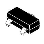
This new series of digital transistors is designed to replace a single device and its external resistor bias network. The BRT (Bias Resistor Transistor) contains a single transistor with a monolithic bias network consisting of two resistors; a series base resistor and a base-emitter resistor. The BRT eliminates these individual components by integrating them into a single device. The use of a BRT can reduce both system cost and board space. The device is housed in the SC-70/SOT-323 package which is designed for low power surface mount applications.
Features http://onsemi.com
NPN SILICON BIAS RESISTOR TRANSISTORS
PIN 3 COLLECTOR (OUTPUT) PIN 2 EMITTER (GROUND)
Simplifies Circuit Design Reduces Board Space Reduces Component Count The SC-70/SOT-323 package can be soldered using wave or reflow. The modified gull-winged leads absorb thermal stress during soldering eliminating the possibility of damage to the die. Available in 8 mm embossed tape and reel. Use the Device Number to order the 7 inch/3000 unit reel. These Devices are Pb--Free, Halogen Free/BFR Free and are RoHS Compliant
MAXIMUM RATINGS (TA = 25C unless otherwise noted)
Rating Collector--Base Voltage Collector--Emitter Voltage Collector Current Symbol VCBO VCEO IC Value 50 50 100 Unit Vdc Vdc mAdc
PIN 1 BASE (INPUT)
R1 R2
3 1
2
SC-70/SOT-323 CASE 419 STYLE 3
MARKING DIAGRAM
THERMAL CHARACTERISTICS
Characteristic Total Device Dissipation TA = 25C Derate above 25C Thermal Resistance, Junction--to--Ambient Thermal Resistance, Junction--to--Lead Junction and Storage Temperature Range Symbol PD Max 202 (Note 1) 310 (Note 2) 1.6 (Note 1) 2.5 (Note 2) 618 (Note 1) 403 (Note 2) 280 (Note 1) 332 (Note 2) -- 55 to +150 Unit mW mW/C C/W C/W C
8x M G G
RθJA RθJL TJ, Tstg
8x = Device Code M = Date Code* G = Pb--Free Package (Note: Microdot may be in either location) *Date Code orientation may vary depending upon manufacturing location.
ORDERING INFORMATION
See detailed ordering and shipping information in the package dimensions section on page 2 of this data sheet.
Stresses exceeding Maximum Ratings may damage the device. Maximum Ratings are stress ratings only. Functional operation above the Recommended Operating Conditions is not implied. Extended exposure to stresses above the Recommended Operating Conditions may affect device reliability. 1. FR--4 @ Minimum Pad. 2. FR--4 @ 1.0 x 1.0 inch Pad.
DEVICE MARKING INFORMATION
See specific marking information in the device marking table on page 2 of this data sheet.
Semiconductor Components Industries, LLC, 2010
October, 2010 - Rev. 9 -
1
Publication Order Number: MUN5211T1/D
�MUN5211T1G Series
DEVICE MARKING AND RESISTOR VALUES
Device MUN5211T1G MUN5212T1G MUN5213T1G MUN5214T1G MUN5215T1G MUN5216T1G (Note 3) MUN5230T1G MUN5231T1G (Note 3) MUN5232T1G MUN5233T1G MUN5234T1G (Note 3) MUN5235T1G MUN5236T1G (Note 3) MUN5237T1G (Note 3) Package SC--70/SOT--323 (Pb--Free) SC--70/SOT--323 (Pb--Free) SC--70/SOT--323 (Pb--Free) SC--70/SOT--323 (Pb--Free) SC--70/SOT--323 (Pb--Free) SC--70/SOT--323 (Pb--Free) SC--70/SOT--323 (Pb--Free) SC--70/SOT--323 (Pb--Free) SC--70/SOT--323 (Pb--Free) SC--70/SOT--323 (Pb--Free) SC--70/SOT--323 (Pb--Free) SC--70/SOT--323 (Pb--Free) SC--70/SOT--323 (Pb--Free) SC--70/SOT--323 (Pb--Free) Marking 8A 8B 8C 8D 8E 8F 8G 8H 8J 8K 8L 8M 8N 8P R1 (K) 10 22 47 10 10 4.7 1.0 2.2 4.7 4.7 22 2.2 100 47 R2 (K) 10 22 47 47 1.0 2.2 4.7 47 47 47 100 22 Shipping† 3000 / Tape & Reel 3000 / Tape & Reel 3000 / Tape & Reel 3000 / Tape & Reel 3000 / Tape & Reel 3000 / Tape & Reel 3000 / Tape & Reel 3000 / Tape & Reel 3000 / Tape & Reel 3000 / Tape & Reel 3000 / Tape & Reel 3000 / Tape & Reel 3000 / Tape & Reel 3000 / Tape & Reel
†For information on tape and reel specifications, including part orientation and tape sizes, please refer to our Tape and Reel Packaging Specifications Brochure, BRD8011/D. 3. New devices. Updated curves to follow in subsequent data sheets.
http://onsemi.com
2
�MUN5211T1G Series
ELECTRICAL CHARACTERISTICS (TA = 25C unless otherwise noted)
Characteristic OFF CHARACTERISTICS Collector--Base Cutoff Current (VCB = 50 V, IE = 0) Collector--Emitter Cutoff Current (VCE = 50 V, IB = 0) Emitter--Base Cutoff Current (VEB = 6.0 V, IC = 0) MUN5211T1G MUN5212T1G MUN5213T1G MUN5214T1G MUN5215T1G MUN5216T1G MUN5230T1G MUN5231T1G MUN5232T1G MUN5233T1G MUN5234T1G MUN5235T1G MUN5236T1G MUN5237T1G ICBO ICEO IEBO ----------------50 50 ------------------100 500 0.5 0.2 0.1 0.2 0.9 1.9 4.3 2.3 1.5 0.18 0.13 0.2 0.05 0.13 --nAdc nAdc mAdc Symbol Min Typ Max Unit
Collector--Base Breakdown Voltage (IC = 10 mA, IE = 0) Collector--Emitter Breakdown Voltage (Note 4) (IC = 2.0 mA, IB = 0) ON CHARACTERISTICS (Note 4) DC Current Gain (VCE = 10 V, IC = 5.0 mA) MUN5211T1G MUN5212T1G MUN5213T1G MUN5214T1G MUN5215T1G MUN5216T1G MUN5230T1G MUN5231T1G MUN5232T1G MUN5233T1G MUN5234T1G MUN5235T1G MUN5236T1G MUN5237T1G MUN5211T1G MUN5212T1G MUN5213T1G MUN5214T1G MUN5236T1G MUN5230T1G MUN5231T1G MUN5237T1G MUN5215T1G MUN5216T1G MUN5232T1G MUN5233T1G MUN5234T1G MUN5235T1G
V(BR)CBO V(BR)CEO
Vdc Vdc
hFE
35 60 80 80 160 160 3.0 8.0 15 80 80 80 80 80 ---------------
60 100 140 140 350 350 5.0 15 30 200 150 140 150 140 ---------------
--------------0.25 0.25 0.25 0.25 0.25 0.25 0.25 0.25 0.25 0.25 0.25 0.25 0.25 0.25 Vdc
Collector--Emitter Saturation Voltage (IC = 10 mA, IB = 0.3 mA)
VCE(sat)
(IC = 10 mA, IB = 5 mA) (IC = 10 mA, IB = 1 mA)
4. Pulse Test: Pulse Width < 300 ms, Duty Cycle < 2.0%
http://onsemi.com
3
�MUN5211T1G Series
ELECTRICAL CHARACTERISTICS (TA = 25C unless otherwise noted) (Continued)
Characteristic ON CHARACTERISTICS (Note 5) (Continued) Output Voltage (on) (VCC = 5.0 V, VB = 2.5 V, RL = 1.0 kΩ) MUN5211T1G MUN5212T1G MUN5214T1G MUN5215T1G MUN5216T1G MUN5230T1G MUN5231T1G MUN5232T1G MUN5233T1G MUN5234T1G MUN5235T1G MUN5213T1G MUN5236T1G MUN5237T1G MUN5211T1G MUN5212T1G MUN5213T1G MUN5214T1G MUN5234T1G MUN5235T1G MUN5230T1G MUN5215T1G MUN5216T1G MUN5231T1G MUN5232T1G MUN5233T1G MUN5236T1G MUN5237T1G MUN5211T1G MUN5212T1G MUN5213T1G MUN5214T1G MUN5215T1G MUN5216T1G MUN5230T1G MUN5231T1G MUN5232T1G MUN5233T1G MUN5234T1G MUN5235T1G MUN5236T1G MUN5237T1G MUN5211T1G MUN5212T1G MUN5213T1G MUN5214T1G MUN5215T1G MUN5216T1G MUN5230T1G MUN5231T1G MUN5232T1G MUN5233T1G MUN5234T1G MUN5235T1G MUN5236T1G MUN5237T1G VOL --------------4.9 4.9 4.9 4.9 4.9 4.9 4.9 4.9 4.9 4.9 4.9 4.9 4.9 4.9 7.0 15.4 32.9 7.0 7.0 3.3 0.7 1.5 3.3 3.3 15.4 1.54 70 32.9 0.8 0.8 0.8 0.17 --0.8 0.8 0.8 0.055 0.38 0.038 0.8 1.7 ----------------------------10 22 47 10 10 4.7 1.0 2.2 4.7 4.7 22 2.2 100 47 1.0 1.0 1.0 0.21 --1.0 1.0 1.0 0.1 0.47 0.047 1.0 2.1 0.2 0.2 0.2 0.2 0.2 0.2 0.2 0.2 0.2 0.2 0.2 0.2 0.2 0.2 --------------13 28.6 61.1 13 13 6.1 1.3 2.9 6.1 6.1 28.6 2.86 130 61.1 1.2 1.2 1.2 0.25 --1.2 1.2 1.2 0.185 0.56 0.056 1.2 2.6 Vdc Symbol Min Typ Max Unit
(VCC = 5.0 V, VB = 3.5 V, RL = 1.0 kΩ) (VCC = 5.0 V, VB = 5.5 V, RL = 1.0 kΩ) (VCC = 5.0 V, VB = 4.0 V, RL = 1.0 kΩ) Output Voltage (off) (VCC = 5.0 V, VB = 0.5 V, RL = 1.0 kΩ)
VOH
Vdc
(VCC = 5.0 V, VB = 0.05 V, RL = 1.0 kΩ) (VCC = 5.0 V, VB = 0.25 V, RL = 1.0 kΩ)
Input Resistor
R1
kΩ
Resistor Ratio
R1/R2
5. Pulse Test: Pulse Width < 300 ms, Duty Cycle < 2.0%
http://onsemi.com
4
�MUN5211T1G Series
350 PD, POWER DISSIPATION (mW) 300 250 200 150 100 50 0 -- 50 RθJA = 403C/W 0 50 100 TA, AMBIENT TEMPERATURE (C) 150
Figure 1. Derating Curve
http://onsemi.com
5
�MUN5211T1G Series
TYPICAL ELECTRICAL CHARACTERISTICS - MUN5211T1G VCE(sat) , MAXIMUM COLLECTOR VOLTAGE (VOLTS) 1 IC/IB = 10 TA = --25C 25C 0.1 75C 1000 hFE , DC CURRENT GAIN (NORMALIZED) VCE = 10 V TA = 75C 25C --25C
100
0.01
0.001
0
20 40 IC, COLLECTOR CURRENT (mA)
50
10
1
10 IC, COLLECTOR CURRENT (mA)
100
Figure 2. VCE(sat) versus IC
Figure 3. DC Current Gain
4 f = 1 MHz IE = 0 V TA = 25C
100 75C IC, COLLECTOR CURRENT (mA) 10 1 0.1
25C TA = --25C
C ob , CAPACITANCE (pF)
3
2
1
0.01 VO = 5 V 0 1 2 3 4 5 6 7 Vin, INPUT VOLTAGE (VOLTS) 8 9 10
0
0
10 20 30 40 VR, REVERSE BIAS VOLTAGE (VOLTS)
50
0.001
Figure 4. Output Capacitance
Figure 5. Output Current versus Input Voltage
10 VO = 0.2 V V in , INPUT VOLTAGE (VOLTS) TA = --25C 25C 75C 1
0.1
0
10
40 20 30 IC, COLLECTOR CURRENT (mA)
50
Figure 6. Input Voltage versus Output Current
http://onsemi.com
6
�MUN5211T1G Series
TYPICAL ELECTRICAL CHARACTERISTICS - MUN5212T1G VCE(sat) , MAXIMUM COLLECTOR VOLTAGE (VOLTS) 1 IC/IB = 10 TA = --25C 25C 75C 1000 hFE , DC CURRENT GAIN (NORMALIZED)
VCE = 10 V TA = 75C 25C --25C
0.1
100
0.01
0.001
0
20 IC, COLLECTOR CURRENT (mA)
40
50
10
1
10 IC, COLLECTOR CURRENT (mA)
100
Figure 7. VCE(sat) versus IC
Figure 8. DC Current Gain
4 f = 1 MHz IE = 0 V TA = 25C
100 IC, COLLECTOR CURRENT (mA) 10 1 0.1 0.01
75C
25C TA = --25C
C ob , CAPACITANCE (pF)
3
2
1
VO = 5 V 0 0 10 20 30 40 VR, REVERSE BIAS VOLTAGE (VOLTS) 50 0.001 0 2 4 6 Vin, INPUT VOLTAGE (VOLTS) 8 10
Figure 9. Output Capacitance
Figure 10. Output Current versus Input Voltage
100 VO = 0.2 V V in , INPUT VOLTAGE (VOLTS) TA = --25C 10 75C 25C
1
0.1
0
10
20
30
40
50
IC, COLLECTOR CURRENT (mA)
Figure 11. Input Voltage versus Output Current
http://onsemi.com
7
�MUN5211T1G Series
TYPICAL ELECTRICAL CHARACTERISTICS - MUN5213T1G VCE(sat) , MAXIMUM COLLECTOR VOLTAGE (VOLTS) 10 IC/IB = 10 1000 hFE , DC CURRENT GAIN (NORMALIZED)
VCE = 10 V TA = 75C 25C --25C
1 TA = --25C 0.1 25C 75C
100
0.01
0
20 40 IC, COLLECTOR CURRENT (mA)
50
10
1
10 IC, COLLECTOR CURRENT (mA)
100
Figure 12. VCE(sat) versus IC
Figure 13. DC Current Gain
1 0.8 C ob , CAPACITANCE (pF)
IC, COLLECTOR CURRENT (mA)
f = 1 MHz IE = 0 V TA = 25C
100 75C 10 1 0.1 0.01
25C TA = --25C
0.6 0.4 0.2 0
VO = 5 V 0 2 4 6 Vin, INPUT VOLTAGE (VOLTS) 8 10
0
10 20 30 40 VR, REVERSE BIAS VOLTAGE (VOLTS)
50
0.001
Figure 14. Output Capacitance
Figure 15. Output Current versus Input Voltage
100 VO = 0.2 V V in , INPUT VOLTAGE (VOLTS) TA = --25C 10 25C 75C
1
0.1
0
10
20
30
40
50
IC, COLLECTOR CURRENT (mA)
Figure 16. Input Voltage versus Output Current
http://onsemi.com
8
�MUN5211T1G Series
TYPICAL ELECTRICAL CHARACTERISTICS - MUN5214T1G VCE(sat) , MAXIMUM COLLECTOR VOLTAGE (VOLTS) 1 TA = --25C 25C 75C hFE , DC CURRENT GAIN (NORMALIZED) IC/IB = 10 300 250 200 150 100 50 0 1 2 4 6 8 10 15 20 40 50 60 70 80 IC, COLLECTOR CURRENT (mA) 90 100 VCE = 10 TA = 75C 25C --25C
0.1
0.01
0.001
0
20 40 60 IC, COLLECTOR CURRENT (mA)
80
Figure 17. VCE(sat) versus IC
Figure 18. DC Current Gain
4 3.5 Cob , CAPACITANCE (pF) 3 2.5 2 1.5 1 0.5 0 0 2 4 6 8 10 15 20 25 30 35 VR, REVERSE BIAS VOLTAGE (VOLTS) 40 45 50 f = 1 MHz lE = 0 V TA = 25C
100 TA = 75C IC, COLLECTOR CURRENT (mA) 25C
--25C 10
VO = 5 V 1 0 2 4 6 Vin, INPUT VOLTAGE (VOLTS) 8 10
Figure 19. Output Capacitance
Figure 20. Output Current versus Input Voltage
10 VO = 0.2 V V in , INPUT VOLTAGE (VOLTS) TA = --25C 25C 75C
1
0.1
0
10
20 30 IC, COLLECTOR CURRENT (mA)
40
50
Figure 21. Input Voltage versus Output Current http://onsemi.com
9
�MUN5211T1G Series
TYPICAL ELECTRICAL CHARACTERISTICS — MUN5215T1G
VCE(sat), COLLECTOR VOLTAGE (VOLTS) 1 IC/IB = 10 hFE, DC CURRENT GAIN 75C --25C 0.01 TA = --25C 25C 1000 75C VCE = 10 V
0.1 25C
100
10
0.001
0
20 40 30 10 IC, COLLECTOR CURRENT (mA)
50
1
1
10 IC, COLLECTOR CURRENT (mA)
100
Figure 22. VCE(sat) versus IC
Figure 23. DC Current Gain
4.5 4 Cob, CAPACITANCE (pF) 3.5 3 2.5 2 1.5 1 0.5 0 0 5 10 15 20 25 30 35 40 45 VR, REVERSE BIAS VOLTAGE (VOLTS) 50 f = 1 MHz IE = 0 V TA = 25C IC, COLLECTOR CURRENT (mA)
100 75C 10 1 0.1 0.01 TA = --25C 25C
VO = 5 V 0 1 2 3 4 5 6 7 8 Vin, INPUT VOLTAGE (VOLTS) 9 10
0.001
Figure 24. Output Capacitance
Figure 25. Output Current versus Input Voltage
10 Vin, INPUT VOLTAGE (VOLTS)
TA = --25C 1 75C 25C
VO = 0.2 V 0.1 0 40 10 20 30 IC, COLLECTOR CURRENT (mA) 50
Figure 26. Input Voltage versus Output Current
http://onsemi.com
10
�MUN5211T1G Series
TYPICAL ELECTRICAL CHARACTERISTICS — MUN5230T1G
VCE(sat), COLLECTOR VOLTAGE (VOLTS) 1 IC/IB = 10 75C --25C hFE, DC CURRENT GAIN 100
0.1 25C
10
75C 25C TA = --25C VCE = 10 V
0.01
0.001
0
10 20 40 30 IC, COLLECTOR CURRENT (mA)
50
1
1
10 IC, COLLECTOR CURRENT (mA)
100
Figure 27. VCE(sat) versus IC
Figure 28. DC Current Gain
4.5 f = 1 MHz IE = 0 V TA = 25C IC, COLLECTOR CURRENT (mA) 4 Cob, CAPACITANCE (pF) 3.5 3 2.5 2 1.5 1 0.5 0 0 5 10 15 20 25 30 35 40 45 VR, REVERSE BIAS VOLTAGE (VOLTS) 50
100 10 1 0.1 0.01
75C 25C
TA = --25C
VO = 5 V 0 1 2 3 4 5 6 7 8 Vin, INPUT VOLTAGE (VOLTS) 9 10
0.001
Figure 29. Output Capacitance
Figure 30. Output Current versus Input Voltage
10 Vin, INPUT VOLTAGE (VOLTS)
TA = --25C 1 75C
25C
VO = 0.2 V 0.1 0 40 10 20 30 IC, COLLECTOR CURRENT (mA) 50
Figure 31. Input Voltage versus Output Current
http://onsemi.com
11
�MUN5211T1G Series
TYPICAL ELECTRICAL CHARACTERISTICS — MUN5232T1G
VCE(sat), COLLECTOR VOLTAGE (VOLTS) 1 IC/IB = 10 hFE, DC CURRENT GAIN 75C --25C 0.01 75C 1000 VCE = 10 V
0.1 25C
100
10
TA = --25C
25C
0.001
0
10 20 40 30 IC, COLLECTOR CURRENT (mA)
50
1
1
10 IC, COLLECTOR CURRENT (mA)
100
Figure 32. VCE(sat) versus IC
Figure 33. DC Current Gain
6 5 4 3 2 1 0 f = 1 MHz IE = 0 V TA = 25C IC, COLLECTOR CURRENT (mA)
100 10 1 0.1 0.01 TA = --25C 75C 25C
Cob, CAPACITANCE (pF)
VO = 5 V 0 1 2 3 4 5 6 7 8 Vin, INPUT VOLTAGE (VOLTS) 9 10
0
5
10 15 20 25 30 35 40 45 VR, REVERSE BIAS VOLTAGE (VOLTS)
50
0.001
Figure 34. Output Capacitance
Figure 35. Output Current versus Input Voltage
10 Vin, INPUT VOLTAGE (VOLTS)
TA = --25C 1
75C
25C
VO = 0.2 V 0.1 0 40 10 20 30 IC, COLLECTOR CURRENT (mA) 50
Figure 36. Input Voltage versus Output Current
http://onsemi.com
12
�MUN5211T1G Series
TYPICAL ELECTRICAL CHARACTERISTICS — MUN5233T1G
VCE(sat), COLLECTOR VOLTAGE (VOLTS) 1 IC/IB = 10 hFE, DC CURRENT GAIN 1000 VCE = 10 V 75C 100 TA = --25C
0.1 --25C 0.01
75C
25C
25C
10
0.001
0
5
10 15 25 20 IC, COLLECTOR CURRENT (mA)
30
1
1
10 IC, COLLECTOR CURRENT (mA)
100
Figure 37. VCE(sat) versus IC
Figure 38. DC Current Gain
4 3.5 Cob, CAPACITANCE (pF) 3 2.5 2 1.5 1 0.5 0 0 5 10 15 20 25 30 35 40 45 VR, REVERSE BIAS VOLTAGE (VOLTS) 50 f = 1 MHz IE = 0 V TA = 25C IC, COLLECTOR CURRENT (mA)
100 10 1
75C 25C
TA = --25C 0.1 0.01
VO = 5 V 0 1 2 3 4 5 6 7 8 Vin, INPUT VOLTAGE (VOLTS) 9 10
0.001
Figure 39. Output Capacitance
Figure 40. Output Current versus Input Voltage
10 Vin, INPUT VOLTAGE (VOLTS)
TA = --25C 1 75C 25C VO = 0.2 V 0.1 0 20 5 10 15 IC, COLLECTOR CURRENT (mA) 25
Figure 41. Input Voltage versus Output Current
http://onsemi.com
13
�MUN5211T1G Series
TYPICAL ELECTRICAL CHARACTERISTICS — MUN5235T1G
VCE(sat), COLLECTOR VOLTAGE (VOLTS) 1 IC/IB = 10 75C --25C 0.01 hFE, DC CURRENT GAIN 1000 75C 100 VCE = 10 V
0.1 25C
TA = --25C
25C
10
0.001
0
10 20 40 30 IC, COLLECTOR CURRENT (mA)
50
1
1
10 IC, COLLECTOR CURRENT (mA)
100
Figure 42. VCE(sat) versus IC
Figure 43. DC Current Gain
4.5 f = 1 MHz IE = 0 V TA = 25C IC, COLLECTOR CURRENT (mA) 4 Cob, CAPACITANCE (pF) 3.5 3 2.5 2 1.5 1 0.5 0 0 5 10 15 20 25 30 35 40 45 VR, REVERSE BIAS VOLTAGE (VOLTS) 50
100 10 1 0.1 0.01
25C 75C
TA = --25C
VO = 5 V 0 1 2 3 4 5 6 7 8 Vin, INPUT VOLTAGE (VOLTS) 9 10
0.001
Figure 44. Output Capacitance
Figure 45. Output Current versus Input Voltage
10 Vin, INPUT VOLTAGE (VOLTS) 75C
1
25C
TA = --25C
VO = 0.2 V 0.1 0 40 10 20 30 IC, COLLECTOR CURRENT (mA) 50
Figure 46. Input Voltage versus Output Current
http://onsemi.com
14
�MUN5211T1G Series
TYPICAL APPLICATIONS FOR NPN BRTs
+12 V
ISOLATED LOAD
FROM mP OR OTHER LOGIC
Figure 47. Level Shifter: Connects 12 or 24 Volt Circuits to Logic
+12 V
VCC
OUT IN LOAD
Figure 48. Open Collector Inverter: Inverts the Input Signal
Figure 49. Inexpensive, Unregulated Current Source
http://onsemi.com
15
�MUN5211T1G Series
PACKAGE DIMENSIONS
SC-70 (SOT-323) CASE 419--04 ISSUE N
D e1
NOTES: 1. DIMENSIONING AND TOLERANCING PER ANSI Y14.5M, 1982. 2. CONTROLLING DIMENSION: INCH. DIM A A1 A2 b c D E e e1 L HE MIN 0.80 0.00 0.30 0.10 1.80 1.15 1.20 0.20 2.00 MILLIMETERS NOM MAX 0.90 1.00 0.05 0.10 0.70 REF 0.35 0.40 0.18 0.25 2.10 2.20 1.24 1.35 1.30 1.40 0.65 BSC 0.38 0.56 2.10 2.40 MIN 0.032 0.000 0.012 0.004 0.071 0.045 0.047 0.008 0.079 INCHES NOM 0.035 0.002 0.028 REF 0.014 0.007 0.083 0.049 0.051 0.026 BSC 0.015 0.083 MAX 0.040 0.004 0.016 0.010 0.087 0.053 0.055 0.022 0.095
3
HE
1 2
E
b e
A 0.05 (0.002) A1
A2 L
c
STYLE 3: PIN 1. BASE 2. EMITTER 3. COLLECTOR
SOLDERING FOOTPRINT*
0.65 0.025 0.65 0.025
1.9 0.075 0.9 0.035 0.7 0.028
SCALE 10:1
mm inches
*For additional information on our Pb--Free strategy and soldering details, please download the ON Semiconductor Soldering and Mounting Techniques Reference Manual, SOLDERRM/D.
ON Semiconductor and are registered trademarks of Semiconductor Components Industries, LLC (SCILLC). SCILLC reserves the right to make changes without further notice to any products herein. SCILLC makes no warranty, representation or guarantee regarding the suitability of its products for any particular purpose, nor does SCILLC assume any liability arising out of the application or use of any product or circuit, and specifically disclaims any and all liability, including without limitation special, consequential or incidental damages. “Typical” parameters which may be provided in SCILLC data sheets and/or specifications can and do vary in different applications and actual performance may vary over time. All operating parameters, including “Typicals” must be validated for each customer application by customer’s technical experts. SCILLC does not convey any license under its patent rights nor the rights of others. SCILLC products are not designed, intended, or authorized for use as components in systems intended for surgical implant into the body, or other applications intended to support or sustain life, or for any other application in which the failure of the SCILLC product could create a situation where personal injury or death may occur. Should Buyer purchase or use SCILLC products for any such unintended or unauthorized application, Buyer shall indemnify and hold SCILLC and its officers, employees, subsidiaries, affiliates, and distributors harmless against all claims, costs, damages, and expenses, and reasonable attorney fees arising out of, directly or indirectly, any claim of personal injury or death associated with such unintended or unauthorized use, even if such claim alleges that SCILLC was negligent regarding the design or manufacture of the part. SCILLC is an Equal Opportunity/Affirmative Action Employer. This literature is subject to all applicable copyright laws and is not for resale in any manner.
PUBLICATION ORDERING INFORMATION
LITERATURE FULFILLMENT: Literature Distribution Center for ON Semiconductor P.O. Box 5163, Denver, Colorado 80217 USA Phone: 303--675--2175 or 800--344--3860 Toll Free USA/Canada Fax: 303--675--2176 or 800--344--3867 Toll Free USA/Canada Email: orderlit@onsemi.com N. American Technical Support: 800--282--9855 Toll Free USA/Canada Europe, Middle East and Africa Technical Support: Phone: 421 33 790 2910 Japan Customer Focus Center Phone: 81--3--5773--3850 ON Semiconductor Website: www.onsemi.com Order Literature: http://www.onsemi.com/orderlit For additional information, please contact your local Sales Representative
http://onsemi.com
16
MUN5211T1/D
�