MUR2100E
Preferred Device
Switch-mode
Power Rectifier
Ultrafast “E” Series with High Reverse
Energy Capability
These state−of−the−art devices are designed for use in switching
power supplies, inverters and as free wheeling diodes.
Features
• 20 mjoules Avalanche Energy Guaranteed
• Excellent Protection Against Voltage Transients in Switching
•
•
•
•
•
•
http://onsemi.com
ULTRAFAST RECTIFIER
2.0 AMPERES, 1000 VOLTS
Inductive Load Circuits
Ultrafast 75 Nanosecond Recovery Time
175°C Operating Junction Temperature
Low Forward Voltage
Low Leakage Current
High Temperature Glass Passivated Junction
These are Pb−Free Devices*
Mechanical Characteristics:
• Case: Epoxy, Molded
• Weight: 0.4 Gram (Approximately)
• Finish: All External Surfaces Corrosion Resistant and Terminal
•
•
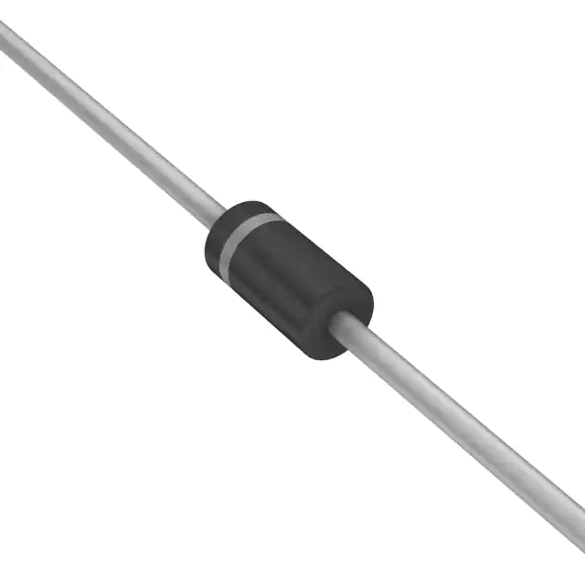
PLASTIC
AXIAL LEAD
CASE 59
Leads are Readily Solderable
Lead Temperature for Soldering Purposes:
260°C Max for 10 Seconds
Polarity: Cathode Indicated by Polarity Band
MARKING DIAGRAM
MAXIMUM RATINGS
Rating
Symbol
Value
Unit
Peak Repetitive Reverse Voltage
Working Peak Reverse Voltage
DC Blocking Voltage
VRRM
VRWM
VR
1000
V
Average Rectified Forward Current (Note 1)
IF(AV)
2.0 @
TA = 35°C
A
Non-Repetitive Peak Surge Current
(Surge applied at rated load conditions,
halfwave, single phase, 60 Hz)
IFSM
35
A
TJ, Tstg
−65 to
+175
°C
Symbol
Value
Unit
RqJA
(Note 3)
°C/W
Operating Junction Temperature and
Storage Temperature Range
Maximum Thermal Resistance,
Junction−to−Ambient
Stresses exceeding Maximum Ratings may damage the device. Maximum
Ratings are stress ratings only. Functional operation above the Recommended
Operating Conditions is not implied. Extended exposure to stresses above the
Recommended Operating Conditions may affect device reliability.
1. Pulse Test: Pulse Width = 300 ms, Duty Cycle ≤ 2.0%.
*For additional information on our Pb−Free strategy and soldering details, please
download the ON Semiconductor Soldering and Mounting Techniques
Reference Manual, SOLDERRM/D.
© Semiconductor Components Industries, LLC, 2006
July, 2006 − Rev. 6
A
= Assembly Location
Y
= Year
WW = Work Week
G
= Pb−Free Package
(Note: Microdot may be in either location)
ORDERING INFORMATION
Package
Shipping†
MUR2100E
Axial Lead**
1000 Units/Bag
MUR2100EG
Axial Lead**
1000 Units/Bag
MUR2100ERL
Axial Lead**
5000/Tape & Reel
MUR2100ERLG
Axial Lead**
5000/Tape & Reel
Device
THERMAL CHARACTERISTICS
Characteristic
A
MUR2100E
YYWW G
G
1
†For information on tape and reel specifications,
including part orientation and tape sizes, please
refer to our Tape and Reel Packaging Specifications
Brochure, BRD8011/D.
**This package is inherently Pb−Free.
Preferred devices are recommended choices for future use
and best overall value.
Publication Order Number:
MUR2100E/D
�MUR2100E
ELECTRICAL CHARACTERISTICS
Characteristic
Symbol
Value
Unit
Maximum Instantaneous Forward Voltage (Note 2)
(IF = 2.0 A, TJ = 150°C)
(IF = 2.0 A, TJ = 25°C)
VF
Maximum Instantaneous Reverse Current (Note 2)
(Rated dc Voltage, TJ = 100°C)
(Rated dc Voltage, TJ = 25°C)
iR
Maximum Reverse Recovery Time
(IF = 1.0 A, di/dt = 50 A/ms)
(IF = 0.5 A, IR = 1.0 A, IREC = 0.25 A)
trr
Maximum Forward Recovery Time
(IF = 1.0 A, di/dt = 100 A/ms, IREC to 1.0 V)
tfr
75
ns
WAVAL
10
mJ
Controlled Avalanche Energy (See Test Circuit in Figure 6)
2. Pulse Test: Pulse Width = 300 ms, Duty Cycle ≤ 2.0%.
IF, INSTANTANEOUS FORWARD
CURRENT (A)
10
VF @ 175°C
150°C
1.0
100°C
25°C
0.1
0.0
0.5
1.0
1.5
2.0
2.5
3.0
3.5
VF, INSTANTANEOUS VOLTAGE (V)
Figure 1. Maximum Forward Voltage
IF, INSTANTANEOUS FORWARD
CURRENT (A)
10
VF @ 175°C
100°C
150°C
1.0
25°C
0.1
0.0
0.5
1.0
1.5
2.0
2.5
3.0
VF, INSTANTANEOUS VOLTAGE (V)
Figure 2. Typical Forward Voltage
http://onsemi.com
2
3.5
1.75
2.20
600
10
100
75
V
mA
ns
�MUR2100E
1.0E−01
1.0E−01
IR, REVERSE CURRENT (A)
IR, REVERSE CURRENT (A)
VR @ 175°C
1.0E−02
1.0E−03 150°C
100°C
1.0E−04
1.0E−05
25°C
1.0E−06
1.0E−07
1.0E−02
1.0E−03
150°C
1.0E−05
100°C
1.0E−06
1.0E−07
1.0E−08
1.0E−08
0
200
400
600
800
VR @ 175°C
1.0E−04
1000
25°C
0
3.0
2.5
DC
1.5
SQUARE WAVE
0.5
0
50
100
150
200
PF(AV), AVERAGE POWER DISSIPATION (A)
3.5
2
SQUARE WAVE
0
0
0.5
40
1
1.5
2
IF(AV), AVERAGE FORWARD CURRENT (A)
Figure 6. Power Dissipation
10
20
DC
1
100
0
1000
3
Figure 5. Current Derating
1
800
4
TA, AMBIENT TEMPERATURE (°C)
C, CAPACITANCE (pF)
IF(AV), AVERAGE FORWARD CURRENT (A)
4.0
0
600
Figure 4. Typical Reverse Current
Figure 3. Maximum Reverse Current
1.0
400
VR, REVERSE VOLTAGE (V)
VR, REVERSE VOLTAGE (V)
2.0
200
60
80
100 120 140 160 180 200
VR, REVERSE VOLTAGE (V)
Figure 7. Typical Capacitance
http://onsemi.com
3
2.5
�MUR2100E
NOTE 3. − AMBIENT MOUNTING DATA
Data shown for thermal resistance, junction−to−ambient
(RqJA) for the mountings shown is to be used as typical
guideline values for preliminary engineering or in case the
tie point temperature cannot be measured.
TYPICAL VALUES FOR RqJA IN STILL AIR
Mounting
Method
1
2
RqJA
Lead Length, L
1/4
1/2
1/8
52
65
72
67
80
87
Units
°C/W
°C/W
50
°C/W
3
MOUNTING METHOD 1
L
L
ÉÉÉÉÉÉÉÉÉÉÉ
MOUNTING METHOD 2
ÉÉÉÉÉÉÉÉÉÉÉÉ
ÉÉÉÉÉÉÉÉÉÉÉÉ
L
L
Vector Pin Mounting
ÉÉ
ÉÉ
ÉÉ
ÉÉ
ÉÉ
ÉÉ
ÉÉ
ÉÉ
MOUNTING METHOD 3
L = 3/8 ″
Board Ground Plane
P.C. Board with
1−1/2 ″ X 1−1/2 ″ Copper Surface
SWITCHMODE is a trademark of Semiconductor Components Industries, LLC.
http://onsemi.com
4
�MECHANICAL CASE OUTLINE
PACKAGE DIMENSIONS
AXIAL LEAD
CASE 59−10
ISSUE U
DATE 15 FEB 2005
B
K
STYLE 1
NOTES:
1. DIMENSIONING AND TOLERANCING PER ANSI
Y14.5M, 1982.
2. CONTROLLING DIMENSION: INCH.
3. ALL RULES AND NOTES ASSOCIATED WITH
JEDEC DO−41 OUTLINE SHALL APPLY
4. POLARITY DENOTED BY CATHODE BAND.
5. LEAD DIAMETER NOT CONTROLLED WITHIN F
DIMENSION.
D
STYLE 2
F
A
SCALE 1:1
POLARITY INDICATOR
OPTIONAL AS NEEDED
(SEE STYLES)
F
K
DIM
A
B
D
F
K
INCHES
MIN
MAX
0.161 0.205
0.079 0.106
0.028 0.034
−−− 0.050
1.000
−−−
MILLIMETERS
MIN
MAX
4.10
5.20
2.00
2.70
0.71
0.86
−−−
1.27
25.40
−−−
GENERIC
MARKING DIAGRAM*
STYLE 1:
PIN 1. CATHODE (POLARITY BAND)
2. ANODE
STYLE 2:
NO POLARITY
A
xxx
xxx
YYWW
STYLE 1
xxx
A
YY
WW
A
xxx
xxx
YYWW
STYLE 2
= Specific Device Code
= Assembly Location
= Year
= Work Week
*This information is generic. Please refer to
device data sheet for actual part marking.
Pb−Free indicator, “G” or microdot “ G”,
may or may not be present.
DOCUMENT NUMBER:
DESCRIPTION:
98ASB42045B
AXIAL LEAD
Electronic versions are uncontrolled except when accessed directly from the Document Repository.
Printed versions are uncontrolled except when stamped “CONTROLLED COPY” in red.
PAGE 1 OF 1
ON Semiconductor and
are trademarks of Semiconductor Components Industries, LLC dba ON Semiconductor or its subsidiaries in the United States and/or other countries.
ON Semiconductor reserves the right to make changes without further notice to any products herein. ON Semiconductor makes no warranty, representation or guarantee regarding
the suitability of its products for any particular purpose, nor does ON Semiconductor assume any liability arising out of the application or use of any product or circuit, and specifically
disclaims any and all liability, including without limitation special, consequential or incidental damages. ON Semiconductor does not convey any license under its patent rights nor the
rights of others.
© Semiconductor Components Industries, LLC, 2019
www.onsemi.com
�onsemi,
, and other names, marks, and brands are registered and/or common law trademarks of Semiconductor Components Industries, LLC dba “onsemi” or its affiliates
and/or subsidiaries in the United States and/or other countries. onsemi owns the rights to a number of patents, trademarks, copyrights, trade secrets, and other intellectual property.
A listing of onsemi’s product/patent coverage may be accessed at www.onsemi.com/site/pdf/Patent−Marking.pdf. onsemi reserves the right to make changes at any time to any
products or information herein, without notice. The information herein is provided “as−is” and onsemi makes no warranty, representation or guarantee regarding the accuracy of the
information, product features, availability, functionality, or suitability of its products for any particular purpose, nor does onsemi assume any liability arising out of the application or use
of any product or circuit, and specifically disclaims any and all liability, including without limitation special, consequential or incidental damages. Buyer is responsible for its products
and applications using onsemi products, including compliance with all laws, regulations and safety requirements or standards, regardless of any support or applications information
provided by onsemi. “Typical” parameters which may be provided in onsemi data sheets and/or specifications can and do vary in different applications and actual performance may
vary over time. All operating parameters, including “Typicals” must be validated for each customer application by customer’s technical experts. onsemi does not convey any license
under any of its intellectual property rights nor the rights of others. onsemi products are not designed, intended, or authorized for use as a critical component in life support systems
or any FDA Class 3 medical devices or medical devices with a same or similar classification in a foreign jurisdiction or any devices intended for implantation in the human body. Should
Buyer purchase or use onsemi products for any such unintended or unauthorized application, Buyer shall indemnify and hold onsemi and its officers, employees, subsidiaries, affiliates,
and distributors harmless against all claims, costs, damages, and expenses, and reasonable attorney fees arising out of, directly or indirectly, any claim of personal injury or death
associated with such unintended or unauthorized use, even if such claim alleges that onsemi was negligent regarding the design or manufacture of the part. onsemi is an Equal
Opportunity/Affirmative Action Employer. This literature is subject to all applicable copyright laws and is not for resale in any manner.
PUBLICATION ORDERING INFORMATION
LITERATURE FULFILLMENT:
Email Requests to: orderlit@onsemi.com
onsemi Website: www.onsemi.com
◊
TECHNICAL SUPPORT
North American Technical Support:
Voice Mail: 1 800−282−9855 Toll Free USA/Canada
Phone: 011 421 33 790 2910
Europe, Middle East and Africa Technical Support:
Phone: 00421 33 790 2910
For additional information, please contact your local Sales Representative
�