Switch-mode
Power Rectifier
MUR550APFG,
MURD550PFG,
MUR550PFG,
MURF550PFG,
NRVUD550PFT4G,
NRVUD550PFT4G-VF01
www.onsemi.com
ULTRAFAST RECTIFIER
5.0 AMPERES, 520 VOLTS
MARKING DIAGRAMS
These state−of−the−art devices are designed for power factor
correction in discontinuous and critical conduction mode.
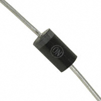
AXIAL LEAD
CASE 267
STYLE 1
Features
•
•
•
•
•
•
•
520 V Rating Meets 80% Derating Requirements of Major OEMs
Low Forward Voltage Drop
Low Leakage
Ultrafast 95 Nanosecond Recovery Time
Reduces Forward Conduction Loss
NRVUD Prefix for Automotive and Other Applications Requiring
Unique Site and Control Change Requirements; AEC−Q101
Qualified and PPAP Capable
These Devices are Pb−Free, Halogen Free/BFR Free and are RoHS
Compliant
A
MUR
550APF
YYWW G
G
DPAK
CASE 369C
STYLE 8
4
1 2
AYWW
U
550G
1
3
4
3
Pin 1: No Connect
Applications
4
• DCM PFC Designs
• Switching Power Supplies
• Power Inverters
TO−220AC
CASE 221B
STYLE 1
AY WWG
MUR550PF
KA
1
Mechanical Characteristics:
• Case: Epoxy, Molded
• Epoxy Meets UL 94 V−0 @ 0.125 in
• Weight: MUR550APFG: 1.1 Gram (Approximately)
•
•
4
3
1
3
MURD550PFG, NRVUD550PFT4G,
NRVUD550PFT4G−VF01: 0.4 Gram
(Approximately)
MUR550PFG, MURF550PFG: 1.9 Gram
(Approximately)
Finish: All External Surfaces Corrosion Resistant and Terminal
Leads are Readily Solderable
Lead and Mounting Surface Temperature for Soldering Purposes:
260°C Max. for 10 Seconds
4
TO−220FP
CASE 221E
STYLE 1
1
4
1
3
A
YY, Y
WW
G or G
KA
3
AYWWG
MURF550PF
KA
= Assembly Location*
= Year
= Work Week
= Pb−Free Package
= Diode Polarity
*The Assembly Location Code (A) is front side
optional. In cases where the Assembly Location is
stamped in the package bottom (molding ejecter
pin), the front side assembly code may be blank.
(Note: Microdot may be in either location)
© Semiconductor Components Industries, LLC, 2012
August, 2020 − Rev. 11
1
Publication Order Number:
MUR550/D
�MUR550APFG, MURD550PFG, MUR550PFG, MURF550PFG, NRVUD550PFT4G,
ORDERING INFORMATION
Device
Shipping†
Package
MUR550APFG
Axial
500 Units/Bag
MUR550APFRLG
Axial
1,500 Tape & Reel
MURD550PFT4G
DPAK
(Pb−Free)
2,500 Tape & Reel
NRVUD550PFT4G*
DPAK
(Pb−Free)
2,500 Tape & Reel
NRVUD550PFT4G−VF01*
DPAK
(Pb−Free)
50 Units / Rail
MUR550PFG
TO−220AC
(Pb−Free)
50 Units / Rail
MURF550PFG
TO−220FP
(Pb−Free)
50 Units / Rail
†For information on tape and reel specifications, including part orientation and tape sizes, please refer to our Tape and Reel Packaging
Specification Brochure, BRD8011/D.
*NRVUD Prefix for Automotive and Other Applications Requiring Unique Site and Control Change Requirements; AEC−Q101 Qualified and
PPAP Capable.
MAXIMUM RATINGS
Rating
Peak Repetitive Reverse Voltage
Working Peak Reverse Voltage
DC Blocking Voltage
Average Rectified Forward Current
(Rated VR) TC = 65°C
(Rated VR) TC = 160°C
MUR550APFG, NRVUD550PFT4G−VF01
MURD550PFG, NRVUD550PFT4G,
MUR550PFG, MURF550PFG
Non−Repetitive Peak Surge Current
(Surge Applied at Rated Load Conditions Halfwave, 60 Hz)
MUR550APFG
NRVUD550PFT4G, NRVUD550PFT4G−VF01, MURD550PFG
MUR550PFG, MURF550PFG
Operating Junction Temperature Range
Symbol
Value
Unit
VRRM
VRWM
VR
520
V
IF(AV)
IFSM
5.0
5.0
85
75
100
A
A
TJ
−65 to +175
°C
Storage Temperature Range
Tstg
−65 to +175
°C
ESD Ratings:
ESD
> 400
> 8000
V
Machine Model = C
Human Body Model = 3B
Stresses exceeding those listed in the Maximum Ratings table may damage the device. If any of these limits are exceeded, device functionality
should not be assumed, damage may occur and reliability may be affected.
THERMAL CHARACTERISTICS
Characteristic
Symbol
Thermal Resistance, Junction−to−Case (Note 1)
MURD550PG, MUR550PFG, NRVUD550PFT4G, NRVUD550PFT4G−VF01
MURF550PFG
RqJC
Thermal Resistance, Junction−to−Ambient
RqJA
MUR550APFG
NRVUD550PFT4G, NRVUD550PFT4G−VF01, MURD550PFG (Note 3),
MURF550PFG
1. Rating applies when surface mounted on the minimum pad sizes recommended.
2. See Note 2, Ambient Mounting Data.
3. 1 inch square pad size on FR4 board.
www.onsemi.com
2
Value
2.8
5.75
Note 2
62
75
Unit
°C/W
°C/W
�MUR550APFG, MURD550PFG, MUR550PFG, MURF550PFG, NRVUD550PFT4G,
ELECTRICAL CHARACTERISTICS
Characteristic
Symbol
Maximum Instantaneous Forward Voltage Drop (Note 4)
(IF = 5.0 A, TJ = 25°C)
(IF = 5.0 A, TJ = 150°C)
VF
Maximum Instantaneous Reverse Current (Note 4)
(VR = 520 V, TJ = 25°C)
(VR = 520 V, TJ = 150°C)
IR
Maximum Reverse Recovery Time (IF = 1.0 A, di/dt = 50 A/ms, VR = 30 V, TJ = 25°C)
trr
Value
1.15
0.98
5.0
400
95
Unit
V
mA
ns
Product parametric performance is indicated in the Electrical Characteristics for the listed test conditions, unless otherwise noted. Product
performance may not be indicated by the Electrical Characteristics if operated under different conditions.
4. Pulse Test: Pulse Width = 300 ms, Duty Cycle ≤ 2.0%.
www.onsemi.com
3
�MUR550APFG, MURD550PFG, MUR550PFG, MURF550PFG, NRVUD550PFT4G,
NOTE 2 — AMBIENT MOUNTING DATA
Data shown for thermal resistance junction−to−ambient
(RqJA) for the mountings shown is to be used as typical
guideline values for preliminary engineering or in case the
tie point temperature cannot be measured.
TYPICAL VALUES FOR RqJA IN STILL AIR
Mounting
Method
1
2
RqJA
Lead Length, L (IN)
1/8
1/4
1/2
3/4
55
50
51
53
63
58
59
61
Units
°C/W
°C/W
28
°C/W
3
MOUNTING METHOD 1
P.C. Board Where Available Copper
Surface area is small.
L
L
ÉÉÉÉÉÉÉÉÉÉÉ
ÉÉÉÉÉÉÉÉÉÉÉ
MOUNTING METHOD 2
Vector Push−In Terminals T−28
L
L
ÉÉÉÉÉÉÉÉÉÉÉÉ
MOUNTING METHOD 3
P.C. Board with
1−1/2 ″ x 1−1/2 ″ Copper Surface
ÉÉ
ÉÉ
ÉÉ
ÉÉ
ÉÉ
ÉÉ
ÉÉ
ÉÉ
L = 1/2 ″
Board Ground Plane
www.onsemi.com
4
�IF, INSTANTANEOUS FORWARD CURRENT (AMPS)
iF, INSTANTANEOUS FORWARD CURRENT (AMPS)
MUR550APFG, MURD550PFG, MUR550PFG, MURF550PFG, NRVUD550PFT4G,
100
100
10
150°C
1.0
0.1
125°C
0.2
0
25°C
0.4
0.6
0.8
1.0
1.4
1.2
1.6
vF, INSTANTANEOUS FORWARD VOLTAGE (VOLTS)
10
150°C
1.0
0.1
125°C
0
0.2
0.4
1.4
1.2
1.6
IR, MAXIMUM REVERSE CURRENT (AMPS)
1.0E−3
IR, REVERSE CURRENT (AMPS)
1.0E−4
150°C
1.0E−4
150°C
125°C
1.0E−5
1.0E−5
125°C
1.0E−6
1.0E−6
1.0E−7
1.0E−7
25°C
1.0E−8
0
100
200
25°C
1.0E−8
500
400
300
1.0E−9
0
100
200
300
500
400
VR, REVERSE VOLTAGE (VOLTS)
VR, REVERSE VOLTAGE (VOLTS)
Figure 3. Typical Reverse Current
Figure 4. Maximum Reverse Current
10
10
PFO, AVERAGE POWER DISSIPATION
(WATTS)
IF, AVERAGE FORWARD CURRENT (AMPS)
1.0
0.8
Figure 2. Maximum Forward Voltage
1.0E−3
dc
SQUARE WAVE
5
0
100
0.6
VF, MAXIMUM INSTANTANEOUS FORWARD VOLTAGE
(VOLTS)
Figure 1. Typical Forward Voltage
1.0E−9
25°C
110
120
130
140
150
160
170
180
9
8
SQUARE
WAVE
7
6
dc
5
4
3
2
1
0
0
1
2
3
4
5
6
7
8
9
TC, CASE TEMPERATURE (°C)
IO, AVERAGE FORWARD CURRENT (AMPS)
Figure 5. Current Derating
Figure 6. Forward Power Dissipation
www.onsemi.com
5
10
�MUR550APFG, MURD550PFG, MUR550PFG, MURF550PFG, NRVUD550PFT4G,
C, CAPACITANCE (pF)
100
25°C
10
1
0
50
100
200
150
VR, REVERSE VOLTAGE (VOLTS)
R(t), TRANSIENT THERMAL RESISTANCE
Figure 7. Capacitance
100
10
0.5
0.2
0.1
0.05
1
0.01
P(pk)
t1
0.1
t2
Single Pulse
0.01
0.000001
0.00001
DUTY CYCLE, D = t1/t2
0.0001
0.001
0.1
0.01
1.0
100
10
1000
t, TIME (s)
R(t), TRANSIENT THERMAL RESISTANCE
Figure 8. Thermal Response for MUR550APFG
10
0.5
1
0.1
0.2
0.1
0.05
0.01
P(pk)
t1
Single Pulse
t2
DUTY CYCLE, D = t1/t2
0.01
0.000001
0.00001
0.0001
0.001
0.01
0.1
1.0
10
100
t, TIME (s)
Figure 9. Thermal Response for MURD550PFG, NRVUD550PFT4G, NRVUD550PFT4G−VF01
www.onsemi.com
6
1000
�R(t), TRANSIENT THERMAL RESISTANCE
MUR550APFG, MURD550PFG, MUR550PFG, MURF550PFG, NRVUD550PFT4G,
10
0.5
1
0.2
0.1
0.05
0.1
0.01
P(pk)
t1
Single Pulse
t2
DUTY CYCLE, D = t1/t2
0.01
0.000001
0.00001
0.0001
0.001
0.01
1.0
0.1
10
100
1000
t, TIME (s)
Figure 10. Thermal Response for MUR550PFG
r(t), TRANSIENT THERMAL RESPONSE
(NORMALIZED) (°C/W)
10
D = 0.5
1.0
0.1
0.2
0.1
0.05
0.02
P(pk)
0.01
SINGLE PULSE
0.01
t1
t2
DUTY CYCLE, D = t1/t2
0.001
0.000001
0.00001
0.0001
0.001
0.01
t, TIME (s)
0.1
1.0
ZqJC(t) = r(t) RqJC
RqJC = 1.6°C/W MAX
D CURVES APPLY FOR POWER
PULSE TRAIN SHOWN
READ TIME AT t1
TJ(pk) - TC = P(pk) ZqJC(t)
10
100
1000
Figure 11. Thermal Response, (MURF550PFG) Junction−to−Case (RqJC)
r(t), TRANSIENT THERMAL RESPONSE
(NORMALIZED) (°C/W)
100
10
D = 0.5
0.2
0.1
0.05
0.02
1.0
0.01
P(pk)
0.1
0.01
0.001
0.000001
t1
SINGLE PULSE
0.00001
t2
DUTY CYCLE, D = t1/t2
0.0001
0.001
0.01
t, TIME (s)
0.1
1.0
ZqJC(t) = r(t) RqJC
RqJC = 1.6°C/W MAX
D CURVES APPLY FOR POWER
PULSE TRAIN SHOWN
READ TIME AT t1
TJ(pk) - TC = P(pk) ZqJC(t)
10
Figure 12. Thermal Response, (MURF550PFG) Junction−to−Ambient (RqJA)
www.onsemi.com
7
100
1000
�MECHANICAL CASE OUTLINE
PACKAGE DIMENSIONS
TO-220 FULLPAK, 2-LEAD
CASE 221E-01
ISSUE A
DATE 21 JAN 2008
SEATING
PLANE
-T-B-
F
NOTES:
1. DIMENSIONING AND TOLERANCING PER ANSI
Y14.5M, 1982.
2. CONTROLLING DIMENSION: INCH.
C
S
SCALE 1:1
Q
U
A
1 2 3
H
-Y-
K
G
N
L
J
R
D 2 PL
0.25 (0.010)
M
B
M
DIM
A
B
C
D
F
G
H
J
K
L
N
Q
R
S
U
INCHES
MIN
MAX
0.617
0.633
0.392
0.408
0.177
0.193
0.024
0.039
0.121
0.129
0.100 BSC
0.117
0.133
0.018
0.025
0.499
0.562
0.045
0.060
0.200 BSC
0.122
0.138
0.101
0.117
0.092
0.108
0.255
0.271
MILLIMETERS
MIN
MAX
15.67
16.07
9.96
10.36
4.50
4.90
0.60
1.00
3.08
3.28
2.54 BSC
2.98
3.38
0.45
0.64
12.68
14.27
1.14
1.52
5.08 BSC
3.10
3.50
2.56
2.96
2.34
2.74
6.48
6.88
STYLE 1:
PIN 1. CATHODE
2. N/A
3. ANODE
Y
GENERIC
MARKING DIAGRAM*
AYWWG
xxxxxxxxxx
KA
Rectifier
A
Y
WW
G
xxxxxx
KA
= Assembly Location
= Year
= Work Week
= Pb-Free Package
= Device Code
= Polarity Designator
*This information is generic. Please refer to
device data sheet for actual part marking.
Pb-Free indicator, “G” or microdot “ G”,
may or may not be present.
DOCUMENT NUMBER:
STATUS:
98ASB42851B
ON SEMICONDUCTOR STANDARD
NEW STANDARD:
©� Semiconductor Components Industries, LLC, 2002
October, DESCRIPTION:
2002 - Rev. 0
http://onsemi.com
TO-220 FULLPAK, 2-LEAD 1
Electronic versions are uncontrolled except when
accessed directly from the Document Repository. Printed
versions are uncontrolled except when stamped
“CONTROLLED COPY” in red.
Case Outline Number:
PAGE 1 OFXXX
2
�DOCUMENT NUMBER:
98ASB42851B
PAGE 2 OF 2
ISSUE
A
REVISION
ADDED 2-LEAD TO PACKAGE DESCRIPTION. UPDATED MIN & MAX VALUES
FOR SEVERAL DIMENSIONS. ADDED MARKING DIAGRAM. REQ. BY M.
SCHAGER.
DATE
21 JAN 2008
ON Semiconductor and
are registered trademarks of Semiconductor Components Industries, LLC (SCILLC). SCILLC reserves the right to make changes without further notice
to any products herein. SCILLC makes no warranty, representation or guarantee regarding the suitability of its products for any particular purpose, nor does SCILLC assume any liability
arising out of the application or use of any product or circuit, and specifically disclaims any and all liability, including without limitation special, consequential or incidental damages.
“Typical” parameters which may be provided in SCILLC data sheets and/or specifications can and do vary in different applications and actual performance may vary over time. All
operating parameters, including “Typicals” must be validated for each customer application by customer's technical experts. SCILLC does not convey any license under its patent rights
nor the rights of others. SCILLC products are not designed, intended, or authorized for use as components in systems intended for surgical implant into the body, or other applications
intended to support or sustain life, or for any other application in which the failure of the SCILLC product could create a situation where personal injury or death may occur. Should
Buyer purchase or use SCILLC products for any such unintended or unauthorized application, Buyer shall indemnify and hold SCILLC and its officers, employees, subsidiaries, affiliates,
and distributors harmless against all claims, costs, damages, and expenses, and reasonable attorney fees arising out of, directly or indirectly, any claim of personal injury or death
associated with such unintended or unauthorized use, even if such claim alleges that SCILLC was negligent regarding the design or manufacture of the part. SCILLC is an Equal
Opportunity/Affirmative Action Employer. This literature is subject to all applicable copyright laws and is not for resale in any manner.
©� Semiconductor Components Industries, LLC, 2008
January, 2008 - Rev. 01A
Case Outline Number:
221E
�MECHANICAL CASE OUTLINE
PACKAGE DIMENSIONS
TO−220, 2−LEAD
CASE 221B−04
ISSUE F
NOTES:
1. DIMENSIONING AND TOLERANCING PER ANSI
Y14.5M, 1982.
2. CONTROLLING DIMENSION: INCH.
C
B
Q
SCALE 1:1
F
S
T
DIM
A
B
C
D
F
G
H
J
K
L
Q
R
S
T
U
4
A
1
U
3
H
K
L
R
D
J
G
STYLE 1:
PIN 1.
2.
3.
4.
DOCUMENT NUMBER:
DESCRIPTION:
98ASB42149B
TO−220, 2−LEAD
CATHODE
N/A
ANODE
CATHODE
DATE 12 APR 2013
STYLE 2:
PIN 1.
2.
3.
4.
INCHES
MIN
MAX
0.595
0.620
0.380
0.405
0.160
0.190
0.025
0.039
0.142
0.161
0.190
0.210
0.110
0.130
0.014
0.025
0.500
0.562
0.045
0.060
0.100
0.120
0.080
0.110
0.045
0.055
0.235
0.255
0.000
0.050
MILLIMETERS
MIN
MAX
15.11
15.75
9.65
10.29
4.06
4.82
0.64
1.00
3.61
4.09
4.83
5.33
2.79
3.30
0.36
0.64
12.70
14.27
1.14
1.52
2.54
3.04
2.04
2.79
1.14
1.39
5.97
6.48
0.000
1.27
ANODE
N/A
CATHODE
ANODE
Electronic versions are uncontrolled except when accessed directly from the Document Repository.
Printed versions are uncontrolled except when stamped “CONTROLLED COPY” in red.
PAGE 1 OF 1
ON Semiconductor and
are trademarks of Semiconductor Components Industries, LLC dba ON Semiconductor or its subsidiaries in the United States and/or other countries.
ON Semiconductor reserves the right to make changes without further notice to any products herein. ON Semiconductor makes no warranty, representation or guarantee regarding
the suitability of its products for any particular purpose, nor does ON Semiconductor assume any liability arising out of the application or use of any product or circuit, and specifically
disclaims any and all liability, including without limitation special, consequential or incidental damages. ON Semiconductor does not convey any license under its patent rights nor the
rights of others.
© Semiconductor Components Industries, LLC, 2019
www.onsemi.com
�MECHANICAL CASE OUTLINE
PACKAGE DIMENSIONS
AXIAL LEAD
CASE 267−05
ISSUE G
DATE 06/06/2000
SCALE 1:1
K
D
NOTES:
1. DIMENSIONS AND TOLERANCING PER ANSI
Y14.5M, 1982.
2. CONTROLLING DIMENSION: INCH.
3. 267-04 OBSOLETE, NEW STANDARD 267-05.
A
1
2
B
K
STYLE 1:
PIN 1. CATHODE (POLARITY BAND)
2. ANODE
DOCUMENT NUMBER:
DESCRIPTION:
DIM
A
B
D
K
98ASB42170B
AXIAL LEAD
INCHES
MIN
MAX
0.287
0.374
0.189
0.209
0.047
0.051
1.000
---
MILLIMETERS
MIN
MAX
7.30
9.50
4.80
5.30
1.20
1.30
25.40
---
STYLE 2:
NO POLARITY
Electronic versions are uncontrolled except when accessed directly from the Document Repository.
Printed versions are uncontrolled except when stamped “CONTROLLED COPY” in red.
PAGE 1 OF 1
ON Semiconductor and
are trademarks of Semiconductor Components Industries, LLC dba ON Semiconductor or its subsidiaries in the United States and/or other countries.
ON Semiconductor reserves the right to make changes without further notice to any products herein. ON Semiconductor makes no warranty, representation or guarantee regarding
the suitability of its products for any particular purpose, nor does ON Semiconductor assume any liability arising out of the application or use of any product or circuit, and specifically
disclaims any and all liability, including without limitation special, consequential or incidental damages. ON Semiconductor does not convey any license under its patent rights nor the
rights of others.
© Semiconductor Components Industries, LLC, 2019
www.onsemi.com
�MECHANICAL CASE OUTLINE
PACKAGE DIMENSIONS
DPAK (SINGLE GAUGE)
CASE 369C
ISSUE F
4
1 2
DATE 21 JUL 2015
3
SCALE 1:1
A
E
b3
C
A
B
c2
4
L3
Z
D
1
L4
2
3
NOTE 7
b2
e
c
SIDE VIEW
b
0.005 (0.13)
TOP VIEW
H
DETAIL A
M
BOTTOM VIEW
C
Z
H
L2
GAUGE
PLANE
C
L
L1
DETAIL A
Z
SEATING
PLANE
BOTTOM VIEW
A1
ALTERNATE
CONSTRUCTIONS
ROTATED 905 CW
STYLE 1:
PIN 1. BASE
2. COLLECTOR
3. EMITTER
4. COLLECTOR
STYLE 6:
PIN 1. MT1
2. MT2
3. GATE
4. MT2
STYLE 2:
PIN 1. GATE
2. DRAIN
3. SOURCE
4. DRAIN
STYLE 7:
PIN 1. GATE
2. COLLECTOR
3. EMITTER
4. COLLECTOR
STYLE 3:
PIN 1. ANODE
2. CATHODE
3. ANODE
4. CATHODE
STYLE 8:
PIN 1. N/C
2. CATHODE
3. ANODE
4. CATHODE
STYLE 4:
PIN 1. CATHODE
2. ANODE
3. GATE
4. ANODE
STYLE 9:
STYLE 10:
PIN 1. ANODE
PIN 1. CATHODE
2. CATHODE
2. ANODE
3. RESISTOR ADJUST
3. CATHODE
4. CATHODE
4. ANODE
SOLDERING FOOTPRINT*
6.20
0.244
2.58
0.102
5.80
0.228
INCHES
MIN
MAX
0.086 0.094
0.000 0.005
0.025 0.035
0.028 0.045
0.180 0.215
0.018 0.024
0.018 0.024
0.235 0.245
0.250 0.265
0.090 BSC
0.370 0.410
0.055 0.070
0.114 REF
0.020 BSC
0.035 0.050
−−− 0.040
0.155
−−−
MILLIMETERS
MIN
MAX
2.18
2.38
0.00
0.13
0.63
0.89
0.72
1.14
4.57
5.46
0.46
0.61
0.46
0.61
5.97
6.22
6.35
6.73
2.29 BSC
9.40 10.41
1.40
1.78
2.90 REF
0.51 BSC
0.89
1.27
−−−
1.01
3.93
−−−
GENERIC
MARKING DIAGRAM*
XXXXXXG
ALYWW
AYWW
XXX
XXXXXG
IC
Discrete
= Device Code
= Assembly Location
= Wafer Lot
= Year
= Work Week
= Pb−Free Package
*This information is generic. Please refer to
device data sheet for actual part marking.
Pb−Free indicator, “G” or microdot “G”, may
or may not be present. Some products may
not follow the Generic Marking.
6.17
0.243
SCALE 3:1
DIM
A
A1
b
b2
b3
c
c2
D
E
e
H
L
L1
L2
L3
L4
Z
XXXXXX
A
L
Y
WW
G
3.00
0.118
1.60
0.063
STYLE 5:
PIN 1. GATE
2. ANODE
3. CATHODE
4. ANODE
NOTES:
1. DIMENSIONING AND TOLERANCING PER ASME
Y14.5M, 1994.
2. CONTROLLING DIMENSION: INCHES.
3. THERMAL PAD CONTOUR OPTIONAL WITHIN DIMENSIONS b3, L3 and Z.
4. DIMENSIONS D AND E DO NOT INCLUDE MOLD
FLASH, PROTRUSIONS, OR BURRS. MOLD
FLASH, PROTRUSIONS, OR GATE BURRS SHALL
NOT EXCEED 0.006 INCHES PER SIDE.
5. DIMENSIONS D AND E ARE DETERMINED AT THE
OUTERMOST EXTREMES OF THE PLASTIC BODY.
6. DATUMS A AND B ARE DETERMINED AT DATUM
PLANE H.
7. OPTIONAL MOLD FEATURE.
mm Ǔ
ǒinches
*For additional information on our Pb−Free strategy and soldering
details, please download the ON Semiconductor Soldering and
Mounting Techniques Reference Manual, SOLDERRM/D.
DOCUMENT NUMBER:
DESCRIPTION:
98AON10527D
DPAK (SINGLE GAUGE)
Electronic versions are uncontrolled except when accessed directly from the Document Repository.
Printed versions are uncontrolled except when stamped “CONTROLLED COPY” in red.
PAGE 1 OF 1
onsemi and
are trademarks of Semiconductor Components Industries, LLC dba onsemi or its subsidiaries in the United States and/or other countries. onsemi reserves
the right to make changes without further notice to any products herein. onsemi makes no warranty, representation or guarantee regarding the suitability of its products for any particular
purpose, nor does onsemi assume any liability arising out of the application or use of any product or circuit, and specifically disclaims any and all liability, including without limitation
special, consequential or incidental damages. onsemi does not convey any license under its patent rights nor the rights of others.
© Semiconductor Components Industries, LLC, 2018
www.onsemi.com
�onsemi,
, and other names, marks, and brands are registered and/or common law trademarks of Semiconductor Components Industries, LLC dba “onsemi” or its affiliates
and/or subsidiaries in the United States and/or other countries. onsemi owns the rights to a number of patents, trademarks, copyrights, trade secrets, and other intellectual property.
A listing of onsemi’s product/patent coverage may be accessed at www.onsemi.com/site/pdf/Patent−Marking.pdf. onsemi reserves the right to make changes at any time to any
products or information herein, without notice. The information herein is provided “as−is” and onsemi makes no warranty, representation or guarantee regarding the accuracy of the
information, product features, availability, functionality, or suitability of its products for any particular purpose, nor does onsemi assume any liability arising out of the application or use
of any product or circuit, and specifically disclaims any and all liability, including without limitation special, consequential or incidental damages. Buyer is responsible for its products
and applications using onsemi products, including compliance with all laws, regulations and safety requirements or standards, regardless of any support or applications information
provided by onsemi. “Typical” parameters which may be provided in onsemi data sheets and/or specifications can and do vary in different applications and actual performance may
vary over time. All operating parameters, including “Typicals” must be validated for each customer application by customer’s technical experts. onsemi does not convey any license
under any of its intellectual property rights nor the rights of others. onsemi products are not designed, intended, or authorized for use as a critical component in life support systems
or any FDA Class 3 medical devices or medical devices with a same or similar classification in a foreign jurisdiction or any devices intended for implantation in the human body. Should
Buyer purchase or use onsemi products for any such unintended or unauthorized application, Buyer shall indemnify and hold onsemi and its officers, employees, subsidiaries, affiliates,
and distributors harmless against all claims, costs, damages, and expenses, and reasonable attorney fees arising out of, directly or indirectly, any claim of personal injury or death
associated with such unintended or unauthorized use, even if such claim alleges that onsemi was negligent regarding the design or manufacture of the part. onsemi is an Equal
Opportunity/Affirmative Action Employer. This literature is subject to all applicable copyright laws and is not for resale in any manner.
PUBLICATION ORDERING INFORMATION
LITERATURE FULFILLMENT:
Email Requests to: orderlit@onsemi.com
onsemi Website: www.onsemi.com
◊
TECHNICAL SUPPORT
North American Technical Support:
Voice Mail: 1 800−282−9855 Toll Free USA/Canada
Phone: 011 421 33 790 2910
Europe, Middle East and Africa Technical Support:
Phone: 00421 33 790 2910
For additional information, please contact your local Sales Representative
�