N57L5125
Product Preview
32‐tap Digital
Potentiometers (POTs)
with 2‐wire Interface
www.onsemi.com
Description
N57L5125 linear-taper digital POTs perform the same function as a
mechanical potentiometer or a variable resistor. This device consists
of a fixed resistor and a wiper contact with 32-tap points that are
digitally controlled through a 2-wire up/down serial interface.
The N57L5125 is configured as a potentiometer. Three resistance
values are available: 10 kW, 50 kW and 100 kW. All devices are
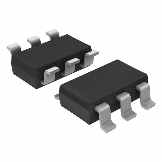
available in a space-saving 6-pin SOT−23 package.
Features
•
•
•
•
•
•
•
•
0.3 mA Ultra-low Standby Current
Single-supply Operation: 2.7 V to 5.5 V
Glitchless Switching between Resistor Taps
Power-on Reset to Midscale
2-wire Up/Down Serial Interface
Resistance Values: 10 kW, 50 kW and 100 kW
Low Wiper Resistance: 80 W
These Devices are Pb-Free, Halogen Free/BFR Free and are RoHS
Compliant
Applications
•
•
•
•
•
MARKING
DIAGRAM
SOT−23
TB SUFFIX
CASE 527AJ
1
XXX
= Specific Device Code
M
= Date Code
G
= Pb−Free Package
(Note: Microdot may be in either location)
PIN CONNECTIONS
SOT−23
VDD 1
6 H
GND 2
5 W
U/D 3
LCD Screen Adjustment
Volume Control
Mechanical Potentiometer Replacement
Gain Adjustment
Line Impedance Matching
XXX MG
G
N57L5125
4 CS
(Top View)
ORDERING INFORMATION
See detailed ordering and shipping information in the package
dimensions section on page 7 of this data sheet.
This document contains information on a product under development. ON Semiconductor
reserves the right to change or discontinue this product without notice.
© Semiconductor Components Industries, LLC, 2016
August, 2016 − Rev. P0
1
Publication Order Number:
N57L5125/D
�N57L5125
H
VDD
U/D
32−POSITION
DECODER
CS
UP−DOWN
COUNTER
GND
W
GND
Figure 1. Functional Diagram
Table 1. PIN DESCRIPTIONS
Pin Number
Pin
Name
Description
1
VDD
Power Supply
2
GND
Ground
3
U/D
Up/Down Control Input. With CS low, a low-to-high transition increments or decrements the wiper
position.
4
CS
Chip Select Input. A high-to-low CS transition determines the mode: increment if U/D is high, or
decrement if U/D is low.
5
W
Wiper Terminal of Resistor
6
H
High Terminal of Resistor
Table 2. ABSOLUTE MAXIMUM RATINGS
Parameters
Ratings
Units
−0.3 to +6
V
−0.3 to (VDD + 0.3)
V
Input and Output Latch−Up Immunity
±200
mA
Maximum Continuous Current into H, L and W
100 kW
50 kW
10 kW
±0.6
±1.3
±1.3
Continuous Power Dissipation (TA = +70°C)
6-pin SC−70 (Note 1)
245
VDD to GND
All Other Pins to GND
mA
mW
Operating Temperature Range
Junction Temperature
Storage Temperature Range
Soldering Temperature (soldering, 10 sec)
−40 to +85
°C
+150
°C
−65 to +150
°C
+300
°C
Stresses exceeding those listed in the Maximum Ratings table may damage the device. If any of these limits are exceeded, device functionality
should not be assumed, damage may occur and reliability may be affected.
1. Derate 3.1 mW/°C above TA = +70°C
www.onsemi.com
2
�N57L5125
Table 3. ELECTRICAL CHARACTERISTICS
(VDD = 2.7 V to 5.5 V, VH = VDD, VL = 0, TA = −40°C to +85°C. Typical values are at VDD = 2.7 V, TA = 25°C, unless otherwise noted.)
Parameter
Symbol
Conditions
Min
Typ
Max
Units
DC PERFORMANCE
Resolution
32
End-to-End Resistance (−00)
80
100
120
End-to-End Resistance (−50)
40
50
60
End-to-End Resistance (−10)
8
10
12
30
300
End-to-End Resistance Tempco
TCR
Ratiometric Resistance Tempco
Taps
5
kW
ppm/°C
ppm/°C
Integral Nonlinearity
INL
±0.5
LSB
Differential Nonlinearity
DNL
±0.5
LSB
±0.1
Full-Scale Error
Zero-Scale Error
Wiper Resistance
RW
80
LSB
1
LSB
200
W
DIGITAL INPUTS
Input High Voltage
VIH
Input Low Voltage
VIL
0.7 x VDD
V
0.3 x VDD
V
TIMING CHARACTERISTICS (Figures 5, 6)
U/D Mode to CS Setup
tCU
25
ns
CS to U/D Step Setup
tCI
50
ns
CS to U/D Step Hold
tIC
25
ns
U/D Step Low Period
tIL
25
ns
U/D Step High Period
tIH
25
ns
Up/Down Toggle Rate (Note 2)
fTOGGLE
Output Settling Time (Note 3)
tSETTLE
1
MHz
100 kW variable resistor
configuration, CL = 10 pF
1
ms
100 kW potentiometer
configuration, CL = 10 pF
0.25
POWER SUPPLY
Supply Voltage
VDD
Active Supply Current (Note 4)
IDD
Standby Supply Current (Note 5)
ISB
2.7
VDD = +5 V
0.3
5.5
V
35
mA
1
mA
Product parametric performance is indicated in the Electrical Characteristics for the listed test conditions, unless otherwise noted. Product
performance may not be indicated by the Electrical Characteristics if operated under different conditions.
2. Up/Down Toggle Rate: fTOGGLE = 1 / tSETTLE
3. Typical settling times are dependent on end-to-end resistance.
4. Supply current measureed while changing wiper tap, fTOGGLE = 500 kHz.
5. Supply current measureed while wiper position is fixed.
www.onsemi.com
3
�N57L5125
TYPICAL OPERATING CHARACTERISTICS
(TA = 25°C, unless otherwise noted.)
0.45
120
0.40
VDD = 5.5 V
0.35
100 k
CURRENT (mA)
RESISTANCE (kW)
100
80
60
50 k
40
0.30
VDD = 2.7 V
0.25
0.20
0.15
0.10
20
10 k
0.05
0
1 3
5
7
0
−50
9 11 13 15 17 19 21 23 25 27 29 31
0
50
100
TAP POSITION
TEMPERATURE (°C)
Figure 2. W-to-GND Resistance vs. Tap
Position
Figure 3. Supply Current vs. Temperature
U/D
2 V/div
WIPER
OUTPUT
100 mV/div
200 ns/div
Figure 4. Tap-to-Tap Switching Transient
www.onsemi.com
4
150
�N57L5125
FUNCTIONAL DESCRIPTION
the mode is set, the device will remain in that mode until CS
goes high again. A low-to-high transition at the U/D pin will
increment or decrement the wiper position depending on the
current mode (Figures 5 and 6).
When the CS input transitions to high (serial interface
inactive), the value of the counter is stored and the wiper
position is maintained.
Note that when the wiper reaches the maximum (or
minimum) tap position, the wiper will not wrap around to the
minimum (or maximum) position.
The N57L5125 consists of a fixed resistor and a wiper
contact with 32−tap points that are digitally controlled
through a 2-wire up/down serial interface. Three end-to-end
resistance values are available: 10 kW, 50 kW and 100 kW.
The N57L5125 is designed to operate as a potentiometer.
In this configuration, the low terminal of the resistor array
is connected to ground (pin 2).
Digital Interface Operation
The devices have two modes of operation when the serial
interface is active: increment and decrement mode. The
serial interface is only active when CS is low.
The CS and U/D inputs control the position of the wiper
along the resistor array. When CS transitions from high to
low, the part will go into increment mode if U/D input is
high, and into decrement mode when U/D input is low. Once
Power-On Reset
All parts in this family feature power-on reset (POR)
circuitry that sets the wiper position to midscale at
power-up. By default, the chip is in the increment mode.
CS
tCU
tIC
tIL
U/D
tIH
tCI
tSETTLE
tSETTLE
W
Note: “W” is not a digital signal. It represents wiper transitions.
Figure 5. Serial Interface Timing Diagram, Increment Mode
CS
tCU
tIC
tIH
U/D
tIL
W
tCI
tSETTLE
tSETTLE
Note: “W” is not a digital signal. It represents wiper transitions.
Figure 6. Serial Interface Timing Diagram, Decrement Mode
www.onsemi.com
5
�N57L5125
APPLICATIONS INFORMATION
Adjustable Gain
The devices are intended for circuits requiring digitally
controlled adjustable resistance, such as LCD contrast
control, where voltage biasing adjusts the display contrast.
Figure 8 shows how to use a potentiometer to digitally
adjust the gain of a noninverting op amp configuration, by
connecting the devices in series with a resistor to ground.
The devices have a low 5 ppm/°C ratiometric tempco that
allows for a very stable adjustable gain configuration over
temperature.
Alternative Positive LCD Bias Control
An op amp can be used to provide buffering and gain on
the output of the N57L5125. This can be done by connecting
the wiper output to the positive input of a noninverting op
amp as shown in Figure 7.
VCC
+5 V
VIN
VOUT
H
30 V
W
VOUT
N57L5125
W
H
N57L5125
Figure 8. Adjustable Gain Circuit
Figure 7. Positive LCD Bias Control
www.onsemi.com
6
�N57L5125
Table 4. ORDERING INFORMATION
Device
N57L5125
Orderable Part Number
Resistor [kW]
Pin Package
Shipping†
N57L5125TBD10TG
10
SOT23−6
3000 / Tape & Reel
N57L5125TBD50TG (Note 7)
50
SOT23−6
3000 / Tape & Reel
N57L5125TBD00TG (Note 7)
100
SOT23−6
3000 / Tape & Reel
†For information on tape and reel specifications, including part orientation and tape sizes, please refer to our Tape and Reel Packaging
Specifications Brochure, BRD8011/D.
6. For detailed information and a breakdown of device nomenclature and numbering systems, please see the ON Semiconductor Device
Nomenclature document, TND310/D, available at www.onsemi.com.
7. Contact factory for availability.
8. All packages are RoHS-compliant (Pb-Free, Halogen-Free).
9. The standard finish is NiPdAu.
10. For additional package and temperature options, please contact your nearest ON Semiconductor Sales office.
www.onsemi.com
7
�N57L5125
PACKAGE DIMENSIONS
D
SOT−23, 6 Lead
CASE 527AJ
ISSUE B
A
NOTES:
1. DIMENSIONING AND TOLERANCING PER
ASME Y14.5M, 1994.
2. CONTROLLING DIMENSION: MILLIMETERS.
3. DATUM C IS THE SEATING PLANE.
B
6
5
4
1
2
3
E
E1
DIM
A
A1
A2
b
c
D
E
E1
e
L
L2
GAGE
PLANE
6X
e
L2
b
0.20
SEATING
PLANE
L
M
C A
S
B
S
DETAIL A
TOP VIEW
A2
c
A
6X
0.10 C
A1
C
SIDE VIEW
MILLIMETERS
MIN
MAX
--1.45
0.00
0.15
0.90
1.30
0.20
0.50
0.08
0.26
2.70
3.00
2.50
3.10
1.30
1.80
0.95 BSC
0.20
0.60
0.25 BSC
SEATING
PLANE
DETAIL A
END VIEW
RECOMMENDED
SOLDERING FOOTPRINT*
3.30
6X
0.85
6X
0.56
0.95
PITCH
DIMENSIONS: MILLIMETERS
*For additional information on our Pb−Free strategy and soldering
details, please download the ON Semiconductor Soldering and
Mounting Techniques Reference Manual, SOLDERRM/D.
ON Semiconductor and
are trademarks of Semiconductor Components Industries, LLC dba ON Semiconductor or its subsidiaries in the United States and/or other countries.
ON Semiconductor owns the rights to a number of patents, trademarks, copyrights, trade secrets, and other intellectual property. A listing of ON Semiconductor’s product/patent
coverage may be accessed at www.onsemi.com/site/pdf/Patent−Marking.pdf. ON Semiconductor reserves the right to make changes without further notice to any products herein.
ON Semiconductor makes no warranty, representation or guarantee regarding the suitability of its products for any particular purpose, nor does ON Semiconductor assume any liability
arising out of the application or use of any product or circuit, and specifically disclaims any and all liability, including without limitation special, consequential or incidental damages.
Buyer is responsible for its products and applications using ON Semiconductor products, including compliance with all laws, regulations and safety requirements or standards,
regardless of any support or applications information provided by ON Semiconductor. “Typical” parameters which may be provided in ON Semiconductor data sheets and/or
specifications can and do vary in different applications and actual performance may vary over time. All operating parameters, including “Typicals” must be validated for each customer
application by customer’s technical experts. ON Semiconductor does not convey any license under its patent rights nor the rights of others. ON Semiconductor products are not
designed, intended, or authorized for use as a critical component in life support systems or any FDA Class 3 medical devices or medical devices with a same or similar classification
in a foreign jurisdiction or any devices intended for implantation in the human body. Should Buyer purchase or use ON Semiconductor products for any such unintended or unauthorized
application, Buyer shall indemnify and hold ON Semiconductor and its officers, employees, subsidiaries, affiliates, and distributors harmless against all claims, costs, damages, and
expenses, and reasonable attorney fees arising out of, directly or indirectly, any claim of personal injury or death associated with such unintended or unauthorized use, even if such
claim alleges that ON Semiconductor was negligent regarding the design or manufacture of the part. ON Semiconductor is an Equal Opportunity/Affirmative Action Employer. This
literature is subject to all applicable copyright laws and is not for resale in any manner.
PUBLICATION ORDERING INFORMATION
LITERATURE FULFILLMENT:
Literature Distribution Center for ON Semiconductor
19521 E. 32nd Pkwy, Aurora, Colorado 80011 USA
Phone: 303−675−2175 or 800−344−3860 Toll Free USA/Canada
Fax: 303−675−2176 or 800−344−3867 Toll Free USA/Canada
Email: orderlit@onsemi.com
N. American Technical Support: 800−282−9855 Toll Free
USA/Canada
Europe, Middle East and Africa Technical Support:
Phone: 421 33 790 2910
Japan Customer Focus Center
Phone: 81−3−5817−1050
www.onsemi.com
8
ON Semiconductor Website: www.onsemi.com
Order Literature: http://www.onsemi.com/orderlit
For additional information, please contact your local
Sales Representative
N57L5125/D
�This datasheet has been downloaded from:
datasheet.eeworld.com.cn
Free Download
Daily Updated Database
100% Free Datasheet Search Site
100% Free IC Replacement Search Site
Convenient Electronic Dictionary
Fast Search System
www.EEworld.com.cn
All Datasheets Cannot Be Modified Without Permission
Copyright © Each Manufacturing Company
�